EP0689265B1 - Low insertion force electrical connection - Google Patents
Low insertion force electrical connection Download PDFInfo
- Publication number
- EP0689265B1 EP0689265B1 EP19950304377 EP95304377A EP0689265B1 EP 0689265 B1 EP0689265 B1 EP 0689265B1 EP 19950304377 EP19950304377 EP 19950304377 EP 95304377 A EP95304377 A EP 95304377A EP 0689265 B1 EP0689265 B1 EP 0689265B1
- Authority
- EP
- European Patent Office
- Prior art keywords
- contact
- pin
- socket connector
- pins
- contacts
- Prior art date
- Legal status (The legal status is an assumption and is not a legal conclusion. Google has not performed a legal analysis and makes no representation as to the accuracy of the status listed.)
- Expired - Lifetime
Links
- 238000003780 insertion Methods 0.000 title description 7
- 230000037431 insertion Effects 0.000 title description 7
- 239000000463 material Substances 0.000 claims description 2
- 230000004308 accommodation Effects 0.000 description 1
- 238000013459 approach Methods 0.000 description 1
- 238000003491 array Methods 0.000 description 1
- 238000013461 design Methods 0.000 description 1
- 238000011161 development Methods 0.000 description 1
- 230000018109 developmental process Effects 0.000 description 1
- 239000002184 metal Substances 0.000 description 1
- 238000012986 modification Methods 0.000 description 1
- 230000004048 modification Effects 0.000 description 1
- 238000012545 processing Methods 0.000 description 1
Images
Classifications
-
- H—ELECTRICITY
- H01—ELECTRIC ELEMENTS
- H01R—ELECTRICALLY-CONDUCTIVE CONNECTIONS; STRUCTURAL ASSOCIATIONS OF A PLURALITY OF MUTUALLY-INSULATED ELECTRICAL CONNECTING ELEMENTS; COUPLING DEVICES; CURRENT COLLECTORS
- H01R13/00—Details of coupling devices of the kinds covered by groups H01R12/70 or H01R24/00 - H01R33/00
- H01R13/02—Contact members
- H01R13/193—Means for increasing contact pressure at the end of engagement of coupling part, e.g. zero insertion force or no friction
-
- H—ELECTRICITY
- H01—ELECTRIC ELEMENTS
- H01R—ELECTRICALLY-CONDUCTIVE CONNECTIONS; STRUCTURAL ASSOCIATIONS OF A PLURALITY OF MUTUALLY-INSULATED ELECTRICAL CONNECTING ELEMENTS; COUPLING DEVICES; CURRENT COLLECTORS
- H01R31/00—Coupling parts supported only by co-operation with counterpart
- H01R31/06—Intermediate parts for linking two coupling parts, e.g. adapter
Definitions
- the invention relates to electrical connection apparatus and more particularly but not exclusively to pin grid array (hereinafter referred to by the usual term of art acronym PGA) sockets which are used for connection with, for example, central processing unit (CPU) chips which normally have in excess of 144 pins.
- PGA pin grid array
- a socket connector for connection to a plurality of pins, which socket connector has a plurality of socket contacts for engagement by the plurality of pins, each socket contact having a pair of contact arms, each arm having a contact point adjacent a free end thereof, the contact points of each contact being staggered such that, in use, a particular pin does not make initial contact with both the contact points of the associated contact simultaneously, and adjacent contacts being positionally staggered with respect to each other such that, in use, the associated pair of adjacent pins does not make initial contact simultaneously with more than one contact point.
- the staggering of the contact points is preferably such that a first contact is made between a first pin of the adjacent pair and one contact point of the contact associated with the first pin, and the next contact is made between the second pin of the adjacent pair and one contact point of the contact associated with the second pin.
- the third contact is preferably made between the first pin and the other contact point of the contact associated with the first pin, and the fourth contact is preferably between the second pin and the other contact point of the contact associated with the second pin.
- Each contact arm preferably has an end portion extending from the contact point to the free end, which end portion lies obliquely to the direction of pin travel to ease the entry of a pin into the associated contact.
- Each contact preferably has a base, the contact arms extending from the base in cantilever fashion.
- Each contact may be formed from sheet material.
- the bases of the contacts may be coplanar, and different contact point spacing from the base plane may be achieved by different lengths of the contact arms.
- a CPU chip is illustrated at 10 and only a small portion is shown from which two pins 11, 12 extend. As discussed previously, a CPU chip has a large number of pins, typically more than 144 and, with further developments in chips, in excess of 200 pins.
- PGA pin grid array
- the contact recesses 15 and 16 are of different depth, the contact recess 16 being deeper than contact recess 15.
- the contact recesses 15 and 16 locate contacts 19, 20 respectively. Again, it would be appreciated that the number of contacts will correspond to the number of pins to the CPU chip.
- the contacts 19 and 20 have pins 21, 22, although it will be appreciated that other forms of electrical connection could be used.
- each recess has a two height ceiling. This provides for accommodation of contacts 19 and 20, both of which have contact arms 23, 24 and 25, 26 respectively of different lengths.
- the contact arms 23 and 24 are of bent metal stamped from a sheet (other way of producing the contacts are possible) and are formed with contact points 30, 31 respectively. Similarly, the contact arms 25 and 26 of the contact 16 are formed with contact points 32, 33 respectively. All four contact points 30, 31, 32 and 33 lie at different distances from upper pin engagement surface 35 of the body portion 14.
- the configuration of the contacts and location of the contact points 30, 31, 32 and 33 are such that as the CPU chip is lowered into engagement with the socket 13, the pin 12 first makes contact with the contact point 32 of the contact 20. With further downward movement of the CPU chip, the pin 11 makes contact with the contact point 30 of the contact 19. Further downward movement of the CPU chip results in contact between the pin 12 and the contact point 33 of the contact 20 and, finally, the pin 11 makes contact with the contact point 31 of the contact 19. In this way, the insertion force of the CPU chip pins into the socket 13 is reduced to approximately a quarter of the force necessary for contacts in which all contact points are level, the greatest force being necessary at initial engagement of a pin with a contact point.
- the contact sequence between the CPU chip pins and the contact points on the contact arms may be different.
- the invention is not limited to engagement of pin grid arrays on CPU chips; indeed, the invention is applicable to any context in which insertion force is a problem in sockets for engagement with multi-pin male connectors.
Landscapes
- Connecting Device With Holders (AREA)
- Coupling Device And Connection With Printed Circuit (AREA)
- Conductive Materials (AREA)
Description
- The invention relates to electrical connection apparatus and more particularly but not exclusively to pin grid array (hereinafter referred to by the usual term of art acronym PGA) sockets which are used for connection with, for example, central processing unit (CPU) chips which normally have in excess of 144 pins.
- A problem arises in connectors with a large number of pins, for example in PGA sockets for connection of CPU chips, in that forces involved in inserting the pins into the sockets are high; this can lead both to difficulty in engagement and to damage. There is also a trend towards increasing the number of pins; for example a 586 chip has in excess of 200 pins.
- Attempts have been made to reduce the insertion force of pins into PGA sockets, for example by arranging socket contacts in two staggered rows. This will reduce insertion force by approximately 50% compared to unstaggered socket contacts. An alternative approach has been to design socket contacts with staggered contact points, such that a pin does not start engagement with both contact arms at the same time, thereby reducing the insertion force. Such a socket contact is disclosed in EP-A-0571105. However such alternatives have not succeeded in reducing insertion force adequately and this invention addresses this problem.
- According to the invention, there is provided a socket connector for connection to a plurality of pins, which socket connector has a plurality of socket contacts for engagement by the plurality of pins, each socket contact having a pair of contact arms, each arm having a contact point adjacent a free end thereof, the contact points of each contact being staggered such that, in use, a particular pin does not make initial contact with both the contact points of the associated contact simultaneously, and adjacent contacts being positionally staggered with respect to each other such that, in use, the associated pair of adjacent pins does not make initial contact simultaneously with more than one contact point.
- The staggering of the contact points is preferably such that a first contact is made between a first pin of the adjacent pair and one contact point of the contact associated with the first pin, and the next contact is made between the second pin of the adjacent pair and one contact point of the contact associated with the second pin.
- The third contact is preferably made between the first pin and the other contact point of the contact associated with the first pin, and the fourth contact is preferably between the second pin and the other contact point of the contact associated with the second pin.
- Each contact arm preferably has an end portion extending from the contact point to the free end, which end portion lies obliquely to the direction of pin travel to ease the entry of a pin into the associated contact.
- Each contact preferably has a base, the contact arms extending from the base in cantilever fashion. Each contact may be formed from sheet material. The bases of the contacts may be coplanar, and different contact point spacing from the base plane may be achieved by different lengths of the contact arms.
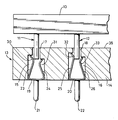
- By way of example, one embodiment of a socket connector according to the invention will now be described with reference to the accompanying drawing, which is a sectional side view of a pair of adjacent contacts in an array of contacts.
- A CPU chip is illustrated at 10 and only a small portion is shown from which two
pins - Part of a pin grid array (PGA) socket is shown at 13, the
socket 13 having abody portion 14 havingcontact recesses pin engagement holes - As can be seen clearly in the drawing, the
contact recesses contact recess 15. Thecontact recesses locate contacts contacts pins - Not only are the
contact recesses contacts contact arms - The
contact arms contact points contact arms contact 16 are formed withcontact points contact points pin engagement surface 35 of thebody portion 14. - The configuration of the contacts and location of the
contact points socket 13, thepin 12 first makes contact with thecontact point 32 of thecontact 20. With further downward movement of the CPU chip, thepin 11 makes contact with thecontact point 30 of thecontact 19. Further downward movement of the CPU chip results in contact between thepin 12 and thecontact point 33 of thecontact 20 and, finally, thepin 11 makes contact with thecontact point 31 of thecontact 19. In this way, the insertion force of the CPU chip pins into thesocket 13 is reduced to approximately a quarter of the force necessary for contacts in which all contact points are level, the greatest force being necessary at initial engagement of a pin with a contact point. - It will be appreciated that the contact sequence between the CPU chip pins and the contact points on the contact arms may be different. Furthermore, it will be appreciated that the invention is not limited to engagement of pin grid arrays on CPU chips; indeed, the invention is applicable to any context in which insertion force is a problem in sockets for engagement with multi-pin male connectors.
- It will be appreciated that different contact point positions can be achieved not only by varying contact arm length but also by locating similar contacts at different positions relative to the pin engagement surface.
- Variations and modifications to the embodiment shown may be made; the embodiment described is by way of example only and the scope of the invention is to be determined by the appended claims.
Claims (7)
- A socket connector (13) for connection to a plurality of pins (11, 12), which socket connector has a plurality of socket contacts (19, 20) for engagement by the plurality of pins each socket contact having a pair of contact arms (23, 24, 25, 26), each arm having a contact point (30, 31, 32, 33) adjacent a free end thereof, the contact points of each contact being staggered such that, in use, a particular pin does not make initial contact with both the contact points of the associated contact simultaneously, and adjacent contacts being positionally staggered with respect to each other such that, in use, the associated pair of adjacent pins does not make initial contact simultaneously with more than one contact point.
- A socket connector as claimed in Claim 1 wherein the staggering of the contact points is such that a first contact is made between a first pin of the adjacent pair and one contact point of the contact associated with the first pin, and the next contact is made between the second pin of the adjacent pair and one contact point of the contact associated with the second pin.
- A socket connector as claimed in Claim 2 wherein the third contact is made between the first pin and the other contact point of the contact associated with the first pin and the fourth contact is between the second pin and the other contact pin of the contact associated with the second pin.
- A socket connector as claimed in any one of Claims 1 to 3 wherein each contact arm has an end portion extending from the contact point to the free end, which end portion lies obliquely to the direction of pin travel.
- A socket connector as claimed in any one of Claims 1 to 4 where each contact has a base, the contact arms extending from the base in cantilever fashion.
- A socket connector as claimed in claim 5 wherein the bases of the contacts are coplanar, different contact point spacing from the base being achieved by different lengths of the contact arms.
- A socket connector as claimed in any one of Claims 1 to 6 wherein each contact is formed from sheet material.
Applications Claiming Priority (2)
| Application Number | Priority Date | Filing Date | Title |
|---|---|---|---|
| GB9412713 | 1994-06-24 | ||
| GB9412713A GB2291279B (en) | 1994-06-24 | 1994-06-24 | Improvements in or relating to electrical connection apparatus |
Publications (2)
| Publication Number | Publication Date |
|---|---|
| EP0689265A1 EP0689265A1 (en) | 1995-12-27 |
| EP0689265B1 true EP0689265B1 (en) | 1997-08-06 |
Family
ID=10757265
Family Applications (1)
| Application Number | Title | Priority Date | Filing Date |
|---|---|---|---|
| EP19950304377 Expired - Lifetime EP0689265B1 (en) | 1994-06-24 | 1995-06-22 | Low insertion force electrical connection |
Country Status (6)
| Country | Link |
|---|---|
| EP (1) | EP0689265B1 (en) |
| JP (1) | JPH0878120A (en) |
| CA (1) | CA2152436C (en) |
| DE (1) | DE69500518T2 (en) |
| ES (1) | ES2107892T3 (en) |
| GB (1) | GB2291279B (en) |
Families Citing this family (2)
| Publication number | Priority date | Publication date | Assignee | Title |
|---|---|---|---|---|
| JP2007250476A (en) * | 2006-03-17 | 2007-09-27 | Espec Corp | Ic socket |
| CN109273880B (en) * | 2018-09-25 | 2020-08-21 | 青岛科技大学 | Electric connection device of flexible circuit board |
Family Cites Families (12)
| Publication number | Priority date | Publication date | Assignee | Title |
|---|---|---|---|---|
| FR2435832A1 (en) * | 1978-07-21 | 1980-04-04 | Alsthom Cgee | ELECTRICAL CONNECTION DEVICE |
| JPS58208222A (en) * | 1982-05-28 | 1983-12-03 | Japan Found Cancer | Enhancing agent for effect of antitumor agent |
| JPS6041342A (en) * | 1983-08-17 | 1985-03-05 | Fujitsu Ltd | Clock selection control system |
| US4591230A (en) * | 1984-06-29 | 1986-05-27 | Frank Roldan | Electrical connector receptacle |
| US4607907A (en) * | 1984-08-24 | 1986-08-26 | Burndy Corporation | Electrical connector requiring low mating force |
| JPH0616415Y2 (en) * | 1988-08-04 | 1994-04-27 | モレックス インコーポレーテッド | Low insertion force electrical connector |
| JPH0616412Y2 (en) * | 1989-07-12 | 1994-04-27 | ホシデン株式会社 | Jack |
| US5004426A (en) * | 1989-09-19 | 1991-04-02 | Teradyne, Inc. | Electrically connecting |
| US4993972A (en) * | 1990-02-07 | 1991-02-19 | Lin Yu C | Multi-purpose PC board connector |
| JP2602385B2 (en) * | 1992-01-16 | 1997-04-23 | 矢崎総業株式会社 | Multi-pole connector |
| JPH0675417B2 (en) * | 1992-05-21 | 1994-09-21 | 山一電機株式会社 | Socket contact |
| JP2672450B2 (en) * | 1993-06-30 | 1997-11-05 | 山一電機株式会社 | Electrical contact |
-
1994
- 1994-06-24 GB GB9412713A patent/GB2291279B/en not_active Expired - Fee Related
-
1995
- 1995-06-22 CA CA 2152436 patent/CA2152436C/en not_active Expired - Fee Related
- 1995-06-22 ES ES95304377T patent/ES2107892T3/en not_active Expired - Lifetime
- 1995-06-22 DE DE1995600518 patent/DE69500518T2/en not_active Expired - Fee Related
- 1995-06-22 EP EP19950304377 patent/EP0689265B1/en not_active Expired - Lifetime
- 1995-06-26 JP JP15954895A patent/JPH0878120A/en active Pending
Also Published As
| Publication number | Publication date |
|---|---|
| JPH0878120A (en) | 1996-03-22 |
| CA2152436C (en) | 2006-08-15 |
| EP0689265A1 (en) | 1995-12-27 |
| DE69500518T2 (en) | 1997-12-11 |
| GB2291279B (en) | 1998-07-15 |
| ES2107892T3 (en) | 1997-12-01 |
| DE69500518D1 (en) | 1997-09-11 |
| CA2152436A1 (en) | 1995-12-25 |
| GB2291279A (en) | 1996-01-17 |
| GB9412713D0 (en) | 1994-09-28 |
Similar Documents
| Publication | Publication Date | Title |
|---|---|---|
| JP2829547B2 (en) | Highly integrated electrical interconnect system | |
| US6485330B1 (en) | Shroud retention wafer | |
| US6193537B1 (en) | Hermaphroditic contact | |
| JP3928075B2 (en) | Electrical interconnection equipment | |
| US5478261A (en) | Modular jack for directly coupling modular plug with printed circuit board | |
| US5462456A (en) | Contact retention device for an electrical connector | |
| US6918776B2 (en) | Mezzanine-type electrical connector | |
| JP2714968B2 (en) | Electrical connector for flat cable | |
| US4558912A (en) | Edge connector for chip carrier | |
| EP0146295B1 (en) | Edge connector for chip carrier and strip of contacts therefor | |
| EP0846350B1 (en) | Method for making surface mountable connectors | |
| EP0340730B1 (en) | Multiple contact assembly for receiving a contact edge of a thin printed circuit card and flexible contact member for this purpose | |
| US4722700A (en) | Low insertion force terminal for use with circuit panel | |
| US6758702B2 (en) | Electrical connector with compression contacts | |
| EP0898793B1 (en) | Depluggable barrier terminal strips | |
| US4932902A (en) | Ultra-high density electrical interconnect system | |
| US4725250A (en) | High density circuit panel socket | |
| EP0299989B1 (en) | High density circuit panel socket | |
| US7775803B2 (en) | Electrical connector having contact retention device | |
| CA2152436C (en) | Improvements in or relating to electrical connection apparatus | |
| US4790779A (en) | Burn-in socket for zig-zag inline semiconductor package | |
| JPH11512556A (en) | Double row composite modular jack for use on board edge | |
| US7445463B2 (en) | Land grid array electrical connector | |
| WO2000070716A1 (en) | Multi way connector | |
| JPH01235177A (en) | Method of forming and arranging contacts in electric connector |
Legal Events
| Date | Code | Title | Description |
|---|---|---|---|
| PUAI | Public reference made under article 153(3) epc to a published international application that has entered the european phase |
Free format text: ORIGINAL CODE: 0009012 |
|
| AK | Designated contracting states |
Kind code of ref document: A1 Designated state(s): BE CH DE ES FR IT LI LU NL SE |
|
| 17P | Request for examination filed |
Effective date: 19960607 |
|
| GRAG | Despatch of communication of intention to grant |
Free format text: ORIGINAL CODE: EPIDOS AGRA |
|
| 17Q | First examination report despatched |
Effective date: 19960923 |
|
| GRAH | Despatch of communication of intention to grant a patent |
Free format text: ORIGINAL CODE: EPIDOS IGRA |
|
| GRAH | Despatch of communication of intention to grant a patent |
Free format text: ORIGINAL CODE: EPIDOS IGRA |
|
| GRAA | (expected) grant |
Free format text: ORIGINAL CODE: 0009210 |
|
| AK | Designated contracting states |
Kind code of ref document: B1 Designated state(s): BE CH DE ES FR IT LI LU NL SE |
|
| PG25 | Lapsed in a contracting state [announced via postgrant information from national office to epo] |
Ref country code: NL Free format text: LAPSE BECAUSE OF FAILURE TO SUBMIT A TRANSLATION OF THE DESCRIPTION OR TO PAY THE FEE WITHIN THE PRESCRIBED TIME-LIMIT Effective date: 19970806 Ref country code: LI Free format text: LAPSE BECAUSE OF FAILURE TO SUBMIT A TRANSLATION OF THE DESCRIPTION OR TO PAY THE FEE WITHIN THE PRESCRIBED TIME-LIMIT Effective date: 19970806 Ref country code: CH Free format text: LAPSE BECAUSE OF FAILURE TO SUBMIT A TRANSLATION OF THE DESCRIPTION OR TO PAY THE FEE WITHIN THE PRESCRIBED TIME-LIMIT Effective date: 19970806 Ref country code: BE Effective date: 19970806 |
|
| REG | Reference to a national code |
Ref country code: CH Ref legal event code: EP |
|
| REF | Corresponds to: |
Ref document number: 69500518 Country of ref document: DE Date of ref document: 19970911 |
|
| ET | Fr: translation filed | ||
| ITF | It: translation for a ep patent filed | ||
| PG25 | Lapsed in a contracting state [announced via postgrant information from national office to epo] |
Ref country code: SE Effective date: 19971106 |
|
| REG | Reference to a national code |
Ref country code: ES Ref legal event code: FG2A Ref document number: 2107892 Country of ref document: ES Kind code of ref document: T3 |
|
| NLV1 | Nl: lapsed or annulled due to failure to fulfill the requirements of art. 29p and 29m of the patents act | ||
| REG | Reference to a national code |
Ref country code: CH Ref legal event code: PL |
|
| PLBE | No opposition filed within time limit |
Free format text: ORIGINAL CODE: 0009261 |
|
| STAA | Information on the status of an ep patent application or granted ep patent |
Free format text: STATUS: NO OPPOSITION FILED WITHIN TIME LIMIT |
|
| 26N | No opposition filed | ||
| REG | Reference to a national code |
Ref country code: FR Ref legal event code: TP Ref country code: FR Ref legal event code: CA |
|
| PGFP | Annual fee paid to national office [announced via postgrant information from national office to epo] |
Ref country code: LU Payment date: 20040325 Year of fee payment: 10 |
|
| PG25 | Lapsed in a contracting state [announced via postgrant information from national office to epo] |
Ref country code: LU Free format text: LAPSE BECAUSE OF NON-PAYMENT OF DUE FEES Effective date: 20050622 |
|
| PGFP | Annual fee paid to national office [announced via postgrant information from national office to epo] |
Ref country code: ES Payment date: 20050708 Year of fee payment: 11 |
|
| PG25 | Lapsed in a contracting state [announced via postgrant information from national office to epo] |
Ref country code: ES Free format text: LAPSE BECAUSE OF NON-PAYMENT OF DUE FEES Effective date: 20060623 |
|
| PGFP | Annual fee paid to national office [announced via postgrant information from national office to epo] |
Ref country code: DE Payment date: 20070731 Year of fee payment: 13 |
|
| REG | Reference to a national code |
Ref country code: ES Ref legal event code: FD2A Effective date: 20060623 |
|
| PGFP | Annual fee paid to national office [announced via postgrant information from national office to epo] |
Ref country code: IT Payment date: 20070626 Year of fee payment: 13 |
|
| PGFP | Annual fee paid to national office [announced via postgrant information from national office to epo] |
Ref country code: FR Payment date: 20070618 Year of fee payment: 13 |
|
| REG | Reference to a national code |
Ref country code: FR Ref legal event code: ST Effective date: 20090228 |
|
| PG25 | Lapsed in a contracting state [announced via postgrant information from national office to epo] |
Ref country code: DE Free format text: LAPSE BECAUSE OF NON-PAYMENT OF DUE FEES Effective date: 20090101 |
|
| PG25 | Lapsed in a contracting state [announced via postgrant information from national office to epo] |
Ref country code: IT Free format text: LAPSE BECAUSE OF NON-PAYMENT OF DUE FEES Effective date: 20080622 Ref country code: FR Free format text: LAPSE BECAUSE OF NON-PAYMENT OF DUE FEES Effective date: 20080630 |