EP0683825B1 - Method for thin film deposition on a substrate using remote cold nitrogen plasma - Google Patents
Method for thin film deposition on a substrate using remote cold nitrogen plasma Download PDFInfo
- Publication number
- EP0683825B1 EP0683825B1 EP94906936A EP94906936A EP0683825B1 EP 0683825 B1 EP0683825 B1 EP 0683825B1 EP 94906936 A EP94906936 A EP 94906936A EP 94906936 A EP94906936 A EP 94906936A EP 0683825 B1 EP0683825 B1 EP 0683825B1
- Authority
- EP
- European Patent Office
- Prior art keywords
- plasma
- substrate
- vessel
- process according
- delayed
- Prior art date
- Legal status (The legal status is an assumption and is not a legal conclusion. Google has not performed a legal analysis and makes no representation as to the accuracy of the status listed.)
- Expired - Lifetime
Links
- 239000000758 substrate Substances 0.000 title claims abstract description 37
- 238000000034 method Methods 0.000 title claims abstract description 35
- IJGRMHOSHXDMSA-UHFFFAOYSA-N Atomic nitrogen Chemical compound N#N IJGRMHOSHXDMSA-UHFFFAOYSA-N 0.000 title claims abstract description 29
- 229910052757 nitrogen Inorganic materials 0.000 title claims abstract description 14
- 238000000427 thin-film deposition Methods 0.000 title 1
- 229910052760 oxygen Inorganic materials 0.000 claims abstract description 18
- 230000015572 biosynthetic process Effects 0.000 claims abstract description 7
- 125000004433 nitrogen atom Chemical group N* 0.000 claims abstract description 7
- 229910052751 metal Inorganic materials 0.000 claims abstract description 4
- 239000002184 metal Substances 0.000 claims abstract description 4
- 150000002902 organometallic compounds Chemical class 0.000 claims abstract 2
- 239000010410 layer Substances 0.000 claims description 24
- 230000008569 process Effects 0.000 claims description 23
- 150000001875 compounds Chemical class 0.000 claims description 22
- 239000007789 gas Substances 0.000 claims description 20
- QVGXLLKOCUKJST-UHFFFAOYSA-N atomic oxygen Chemical compound [O] QVGXLLKOCUKJST-UHFFFAOYSA-N 0.000 claims description 15
- 239000001301 oxygen Substances 0.000 claims description 15
- 230000003111 delayed effect Effects 0.000 claims description 11
- 230000008021 deposition Effects 0.000 claims description 8
- 239000002243 precursor Substances 0.000 claims description 8
- -1 siloxanes Chemical class 0.000 claims description 6
- 230000005495 cold plasma Effects 0.000 claims description 5
- 150000003961 organosilicon compounds Chemical class 0.000 claims description 3
- 239000013047 polymeric layer Substances 0.000 claims description 3
- MYMOFIZGZYHOMD-UHFFFAOYSA-N Dioxygen Chemical compound O=O MYMOFIZGZYHOMD-UHFFFAOYSA-N 0.000 claims description 2
- 125000005595 acetylacetonate group Chemical group 0.000 claims description 2
- 150000001450 anions Chemical class 0.000 claims description 2
- 150000001768 cations Chemical class 0.000 claims description 2
- 229910001882 dioxygen Inorganic materials 0.000 claims description 2
- 238000010494 dissociation reaction Methods 0.000 claims description 2
- 230000005593 dissociations Effects 0.000 claims description 2
- 150000004820 halides Chemical class 0.000 claims description 2
- 238000005215 recombination Methods 0.000 claims description 2
- 230000006798 recombination Effects 0.000 claims description 2
- 125000000082 organogermanium group Chemical group 0.000 claims 1
- 239000000126 substance Substances 0.000 claims 1
- 239000010409 thin film Substances 0.000 abstract description 4
- 238000002161 passivation Methods 0.000 abstract description 2
- 150000002291 germanium compounds Chemical class 0.000 abstract 1
- 210000002381 plasma Anatomy 0.000 description 27
- 239000000203 mixture Substances 0.000 description 8
- VYPSYNLAJGMNEJ-UHFFFAOYSA-N Silicium dioxide Chemical compound O=[Si]=O VYPSYNLAJGMNEJ-UHFFFAOYSA-N 0.000 description 7
- 238000000151 deposition Methods 0.000 description 7
- 229910002808 Si–O–Si Inorganic materials 0.000 description 6
- 230000001464 adherent effect Effects 0.000 description 5
- 150000002500 ions Chemical class 0.000 description 5
- 229910008051 Si-OH Inorganic materials 0.000 description 4
- 229910004298 SiO 2 Inorganic materials 0.000 description 4
- 229910006358 Si—OH Inorganic materials 0.000 description 4
- KPUWHANPEXNPJT-UHFFFAOYSA-N disiloxane Chemical class [SiH3]O[SiH3] KPUWHANPEXNPJT-UHFFFAOYSA-N 0.000 description 4
- 238000005516 engineering process Methods 0.000 description 4
- 150000003254 radicals Chemical class 0.000 description 4
- 229910008338 Si—(CH3) Inorganic materials 0.000 description 3
- 239000000919 ceramic Substances 0.000 description 3
- 230000000694 effects Effects 0.000 description 3
- BOTDANWDWHJENH-UHFFFAOYSA-N Tetraethyl orthosilicate Chemical compound CCO[Si](OCC)(OCC)OCC BOTDANWDWHJENH-UHFFFAOYSA-N 0.000 description 2
- 125000004429 atom Chemical group 0.000 description 2
- 238000006243 chemical reaction Methods 0.000 description 2
- 230000000295 complement effect Effects 0.000 description 2
- 229920006037 cross link polymer Polymers 0.000 description 2
- 229910021419 crystalline silicon Inorganic materials 0.000 description 2
- 239000010408 film Substances 0.000 description 2
- 239000000463 material Substances 0.000 description 2
- 229920000642 polymer Polymers 0.000 description 2
- 229920001296 polysiloxane Polymers 0.000 description 2
- 239000000377 silicon dioxide Substances 0.000 description 2
- 229910052814 silicon oxide Inorganic materials 0.000 description 2
- BLRPTPMANUNPDV-UHFFFAOYSA-N Silane Chemical compound [SiH4] BLRPTPMANUNPDV-UHFFFAOYSA-N 0.000 description 1
- 230000009471 action Effects 0.000 description 1
- 230000015556 catabolic process Effects 0.000 description 1
- 239000011248 coating agent Substances 0.000 description 1
- 238000000576 coating method Methods 0.000 description 1
- 239000008139 complexing agent Substances 0.000 description 1
- 239000002131 composite material Substances 0.000 description 1
- 238000009833 condensation Methods 0.000 description 1
- 230000005494 condensation Effects 0.000 description 1
- 238000006731 degradation reaction Methods 0.000 description 1
- 230000001066 destructive effect Effects 0.000 description 1
- 238000010586 diagram Methods 0.000 description 1
- 239000002019 doping agent Substances 0.000 description 1
- 230000005672 electromagnetic field Effects 0.000 description 1
- 238000000605 extraction Methods 0.000 description 1
- 230000005283 ground state Effects 0.000 description 1
- 238000010438 heat treatment Methods 0.000 description 1
- UQEAIHBTYFGYIE-UHFFFAOYSA-N hexamethyldisiloxane Chemical compound C[Si](C)(C)O[Si](C)(C)C UQEAIHBTYFGYIE-UHFFFAOYSA-N 0.000 description 1
- 229910052500 inorganic mineral Inorganic materials 0.000 description 1
- 238000004519 manufacturing process Methods 0.000 description 1
- 230000008018 melting Effects 0.000 description 1
- 238000002844 melting Methods 0.000 description 1
- 150000002739 metals Chemical class 0.000 description 1
- 238000004377 microelectronic Methods 0.000 description 1
- 239000011707 mineral Substances 0.000 description 1
- 238000012986 modification Methods 0.000 description 1
- 230000004048 modification Effects 0.000 description 1
- 239000000178 monomer Substances 0.000 description 1
- 239000011368 organic material Substances 0.000 description 1
- 239000002245 particle Substances 0.000 description 1
- 230000009257 reactivity Effects 0.000 description 1
- 229910000077 silane Inorganic materials 0.000 description 1
- 230000002459 sustained effect Effects 0.000 description 1
- 239000013598 vector Substances 0.000 description 1
Images
Classifications
-
- C—CHEMISTRY; METALLURGY
- C23—COATING METALLIC MATERIAL; COATING MATERIAL WITH METALLIC MATERIAL; CHEMICAL SURFACE TREATMENT; DIFFUSION TREATMENT OF METALLIC MATERIAL; COATING BY VACUUM EVAPORATION, BY SPUTTERING, BY ION IMPLANTATION OR BY CHEMICAL VAPOUR DEPOSITION, IN GENERAL; INHIBITING CORROSION OF METALLIC MATERIAL OR INCRUSTATION IN GENERAL
- C23C—COATING METALLIC MATERIAL; COATING MATERIAL WITH METALLIC MATERIAL; SURFACE TREATMENT OF METALLIC MATERIAL BY DIFFUSION INTO THE SURFACE, BY CHEMICAL CONVERSION OR SUBSTITUTION; COATING BY VACUUM EVAPORATION, BY SPUTTERING, BY ION IMPLANTATION OR BY CHEMICAL VAPOUR DEPOSITION, IN GENERAL
- C23C16/00—Chemical coating by decomposition of gaseous compounds, without leaving reaction products of surface material in the coating, i.e. chemical vapour deposition [CVD] processes
- C23C16/22—Chemical coating by decomposition of gaseous compounds, without leaving reaction products of surface material in the coating, i.e. chemical vapour deposition [CVD] processes characterised by the deposition of inorganic material, other than metallic material
- C23C16/30—Deposition of compounds, mixtures or solid solutions, e.g. borides, carbides, nitrides
- C23C16/40—Oxides
- C23C16/401—Oxides containing silicon
-
- C—CHEMISTRY; METALLURGY
- C23—COATING METALLIC MATERIAL; COATING MATERIAL WITH METALLIC MATERIAL; CHEMICAL SURFACE TREATMENT; DIFFUSION TREATMENT OF METALLIC MATERIAL; COATING BY VACUUM EVAPORATION, BY SPUTTERING, BY ION IMPLANTATION OR BY CHEMICAL VAPOUR DEPOSITION, IN GENERAL; INHIBITING CORROSION OF METALLIC MATERIAL OR INCRUSTATION IN GENERAL
- C23C—COATING METALLIC MATERIAL; COATING MATERIAL WITH METALLIC MATERIAL; SURFACE TREATMENT OF METALLIC MATERIAL BY DIFFUSION INTO THE SURFACE, BY CHEMICAL CONVERSION OR SUBSTITUTION; COATING BY VACUUM EVAPORATION, BY SPUTTERING, BY ION IMPLANTATION OR BY CHEMICAL VAPOUR DEPOSITION, IN GENERAL
- C23C16/00—Chemical coating by decomposition of gaseous compounds, without leaving reaction products of surface material in the coating, i.e. chemical vapour deposition [CVD] processes
- C23C16/22—Chemical coating by decomposition of gaseous compounds, without leaving reaction products of surface material in the coating, i.e. chemical vapour deposition [CVD] processes characterised by the deposition of inorganic material, other than metallic material
- C23C16/30—Deposition of compounds, mixtures or solid solutions, e.g. borides, carbides, nitrides
- C23C16/40—Oxides
- C23C16/407—Oxides of zinc, germanium, cadmium, indium, tin, thallium or bismuth
-
- C—CHEMISTRY; METALLURGY
- C23—COATING METALLIC MATERIAL; COATING MATERIAL WITH METALLIC MATERIAL; CHEMICAL SURFACE TREATMENT; DIFFUSION TREATMENT OF METALLIC MATERIAL; COATING BY VACUUM EVAPORATION, BY SPUTTERING, BY ION IMPLANTATION OR BY CHEMICAL VAPOUR DEPOSITION, IN GENERAL; INHIBITING CORROSION OF METALLIC MATERIAL OR INCRUSTATION IN GENERAL
- C23C—COATING METALLIC MATERIAL; COATING MATERIAL WITH METALLIC MATERIAL; SURFACE TREATMENT OF METALLIC MATERIAL BY DIFFUSION INTO THE SURFACE, BY CHEMICAL CONVERSION OR SUBSTITUTION; COATING BY VACUUM EVAPORATION, BY SPUTTERING, BY ION IMPLANTATION OR BY CHEMICAL VAPOUR DEPOSITION, IN GENERAL
- C23C16/00—Chemical coating by decomposition of gaseous compounds, without leaving reaction products of surface material in the coating, i.e. chemical vapour deposition [CVD] processes
- C23C16/44—Chemical coating by decomposition of gaseous compounds, without leaving reaction products of surface material in the coating, i.e. chemical vapour deposition [CVD] processes characterised by the method of coating
- C23C16/50—Chemical coating by decomposition of gaseous compounds, without leaving reaction products of surface material in the coating, i.e. chemical vapour deposition [CVD] processes characterised by the method of coating using electric discharges
- C23C16/513—Chemical coating by decomposition of gaseous compounds, without leaving reaction products of surface material in the coating, i.e. chemical vapour deposition [CVD] processes characterised by the method of coating using electric discharges using plasma jets
Definitions
- the present invention relates to a process for producing thin, homogeneous and adherent layers on the surface of metallic, organic or mineral substrates which can be used in the production of electronic or micro-electronic devices.
- the present invention also relates to the products obtained by the process.
- the electronics industry has used materials technology for several decades, involving their electronic, dielectric, conductive or insulating properties.
- the thin film can be obtained by condensation of silicon oxide vapor obtained by bombardment of a target of (SiO 2 ) with a beam of high energy ions.
- Plasma assisted deposition technology in which a plasma gas is excited by a radiofrequency, microwave or continuous discharge.
- Plasma gas is very often composed of rare gas, alone or in mixture at pressures between 10 -5 and 10 -2 hPa.
- This discharge plasma is composed of ionic species, fast electrons, electronically and / or vibrationally excited atoms and / or molecules as well as ultraviolet photons. It is in this medium that the precursor gas of the deposit is introduced.
- the deposit precursor gas is generally composed of a mixture of silane (SiH 4 ) and oxygen or an organo-silica gas such as tetraethoxysilane (TEOS).
- This precursor gas is dissociated by the plasma and the dissociation products, most often radicals, recombine on the surface of the substrate to form the deposit itself.
- Polysiloxanes are obtained in the same way from monomers such as hexamethyldisiloxane for example.
- the main characteristics of this technique are to provide a deposit, the stoichiometry of which is that of the precursor gases. It provides a deposition rate limited by the regasifications induced by the action of the high energy vectors of the plasma (ions, fast electrons and UV photons) and causes a rapid heating of the substrate at temperatures above the melting point of organic materials. conventional (T °> 200 ° C).
- This technique exposes the substrate to significant ionic and electronic bombardments and generates processes of photochemical degradation of the substrate as well as of the deposit formed.
- the effective surface of the deposit is determined by the geometry of the electrodes. These do not exceed a few hundred square centimeters.
- the very high viscosity of this type of plasma limits the application of this technique to deposits on flat surfaces and prevents the deposit from being carried out correctly on left surfaces.
- the present invention aims to provide a method enabling a thin polymeric layer to be deposited on metallic, inorganic or polymeric substrates at high processing speeds.
- the deposits produced according to the present invention have the property of being homogeneous and adherent to the substrate.
- Another object of this invention is to provide a process which can achieve at will a thin and homogeneous deposit on a flat substrate as well as a homogeneous film on substrates with complex geometry, in particular in three dimensions.
- the method for applying a thin polymeric layer to a metallic, inorganic or organic substrate in which a delayed nitrogen plasma consisting essentially of nitrogen atoms is produced in an enclosure in which the substrate is located. free, characterized in that a gaseous organo-siliceous or germanized compound is introduced into said enclosure during the formation of the nitrogen-deferred plasma, containing CH, Si (or Ge), O or NH groups.
- the above process makes it possible to produce, in an area remote from the discharge area, a plasma consisting essentially of free nitrogen atoms.
- the nitrogen plasma has the effect of treating the surface of the substrate to make it adherent with respect to a coating applied subsequently, that is to say to outside the processing enclosure.
- the presence of the organosilicate or germanized compound in the plasma enclosure makes it possible to obtain on the substrate a layer which can adhere to any substrate.
- the speed of formation of this layer is rapid because it is generated in a medium devoid of destructive ionic or photonic bombardment effects with regard to the formation of the layer.
- said siliceous gaseous compound is chosen from alkoxysilanes, siloxanes and silazanes.
- a gaseous compound containing oxygen is added to the gaseous compound introduced into the enclosure and outside the discharge.
- This gaseous oxygen-containing compound can be molecular oxygen.
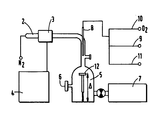
- the single appended figure given by way of nonlimiting example shows the diagram of a device for implementing the method according to the invention.
- a source 1 of nitrogen supply connected to a tube 2 which comprises a cavity 3 in which takes place a sustained discharge and connected to a microwave generator 4.
- the nitrogen pressure inside the tube 2 is between 1 and 20 hPa.
- the frequency generated by the microwave generator can be equal to 2450, 915, 433 MHz or any other legal frequency.
- the tube 2 is connected to a treatment enclosure 5 provided with a gauge 6 for measuring the pressure.
- the enclosure 5 is connected to a vacuum pump 7.
- an injector 8 used to inject into the enclosure 5 a gaseous organo-siliceous compound 9, of oxygen 10 or another complementary reactive gas 11.
- a substrate 12 Inside the enclosure 5 is located a substrate 12 on which we want to deposit a thin dielectric layer and strongly adherent.
- the cold plasma delayed in flow is initiated by the effect of the microwave discharge on the plasma gas consisting of nitrogen (N2) possibly doped and expanded in the tube called "discharge tube".
- N2 nitrogen
- the cold plasma delayed in flow is obtained by extraction, in dynamic regime and in enclosure 5 located outside the electromagnetic field, of the excited species of the discharge (electrons, ions, atoms, vibrationally or electronically excited molecules).
- This reactive medium is characterized by the fact that it does not contain any appreciable amount of ions or electrons.
- nitrogen plasmas allow them to have a much greater lifetime and extension in volume than those of oxygen plasmas for example.
- plasma gases such as: CO, CO 2 , NO, NO 2 , CO, H 2 O.
- the properties of a cold flowing plasma can be oriented by a doping agent for example: O 2 , NH 3 , NF 3 , CF 4 , SF 6 .
- the method according to the present invention consists in depositing on the surface of the metallic or non-metallic substrate 12 an adherent and homogeneous thin layer. This layer is formed by heterogeneous recombination reactions of radical species on the surface of the substrate. These species result from the reaction between the gaseous precursor (organosilicon compound) and the cold plasma delayed in flow.
- gaseous precursor organosilicon compound
- the substrate 12 When an alkoxysilane is introduced into the plasma chamber 5 and when the oxygen content is greater than a few percent, the substrate 12 a layer of a mixture of amorphous silica and polymerized silica.
- the substrate can be metallic, ceramic or polymer.
- the layer obtained can have a controlled thickness which can be between 500 ⁇ and 50 ⁇ m.
- the deposition rate of the layer can be of the order of 1 ⁇ m / min.
- the substrates coated with such a layer can be used as components comprising a passivation layer for electrical or thermal protection, in particular in on-board electronics.
- the gases introduced are ions (anions or cations comprising metals) placed in the gas phase in the form of halides, oxyhyhalides or complexes such as acetylacetonates, fluoroacetylacetonates, etc. or other complexing agents.
- Composite thin layers are thus formed with controlled electrical or dielectric properties.
Landscapes
- Chemical & Material Sciences (AREA)
- Engineering & Computer Science (AREA)
- Mechanical Engineering (AREA)
- Chemical Kinetics & Catalysis (AREA)
- General Chemical & Material Sciences (AREA)
- Materials Engineering (AREA)
- Metallurgy (AREA)
- Organic Chemistry (AREA)
- Inorganic Chemistry (AREA)
- Physics & Mathematics (AREA)
- Plasma & Fusion (AREA)
- Chemical Vapour Deposition (AREA)
- Photovoltaic Devices (AREA)
- Light Receiving Elements (AREA)
Abstract
Description
La présente invention concerne un procédé pour réaliser des couches minces, homogènes et adhérentes à la surface de substrats métalliques, organiques, ou minéraux pouvant intervenir dans la réalisation de dispositifs électroniques ou micro-électroniques.The present invention relates to a process for producing thin, homogeneous and adherent layers on the surface of metallic, organic or mineral substrates which can be used in the production of electronic or micro-electronic devices.
La présente invention concerne également les produits obtenus par le procédé.The present invention also relates to the products obtained by the process.
L'industrie électronique utilise, depuis plusieurs décennies la technologie des matériaux faisant intervenir leurs propriétés électroniques, diélectriques, conductrices ou isolantes.The electronics industry has used materials technology for several decades, involving their electronic, dielectric, conductive or insulating properties.
Les matériaux utilisés pour les applications électroniques ont subi d'importantes modifications afin de répondre à des soucis de performances dans des conditions d'utilisation de plus en plus sévères. Ces modifications ont poussé les industries électroniques à opérer d'importantes miniaturisations de l'ensemble de leurs composants. Ceux-ci ont donc été amenés à être présentés en couches de plus en plus minces faisant intervenir des technologies de dépôt nouvelles.The materials used for electronic applications have undergone significant modifications in order to respond to performance concerns under increasingly severe conditions of use. These changes have prompted the electronics industries to operate major miniaturizations of all of their components. These have therefore been brought to be presented in increasingly thinner layers involving new deposition technologies.
Parmi celles-ci, nous retenons essentiellement les technologies consistant à déposer sur un substrat métallique, un dépôt d'un oxyde de silicium (SiO2), ou d'un composé à caractère céramique ou polymérique tel SiN ou de polysiloxanes. Celui-ci peut être réalisé de plusieurs manières différentes.Among these, we essentially retain the technologies consisting of depositing on a metal substrate, a deposit of a silicon oxide (SiO 2 ), or of a compound of ceramic or polymeric nature such as SiN or of polysiloxanes. This can be done in several different ways.
Par exemple pour SiO2, le film mince peut être obtenu par condensation de vapeur d'oxyde de silicium obtenue par bombardement d'une cible de (SiO2) par un faisceau d'ions de grande énergie.For example for SiO 2 , the thin film can be obtained by condensation of silicon oxide vapor obtained by bombardment of a target of (SiO 2 ) with a beam of high energy ions.
Certains auteurs utilisent, pour créer un film de (SiO2), la technologie de dépôt assisté par plasma dans laquelle un gaz plasmagène est excité par une décharge radiofréquence, micro-onde ou continue. Le gaz plasmagène est très souvent composé de gaz rare, seul ou en mélange à des pressions comprises entre 10-5 et 10-2 hPa. Ce plasma de décharge est composé d'espèces ioniques, d'électrons rapides, d'atomes et/ou de molécules électroniquement et/ou vibrationnellement excitées ainsi que de photons ultraviolets. C'est dans ce milieu qu'est introduit le gaz précurseur du dépôt. Le gaz précurseur du dépôt est généralement composé d'un mélange de silane (SiH4) et d'oxygène ou d'un gaz organo silicé tel que le tétraéthoxysilane (TEOS). Ce gaz précurseur est dissocié par le plasma et les produits de dissociation, le plus souvent radicalaires, se recombinent à la surface du substrat pour former le dépôt proprement dit. Des polysiloxanes sont obtenus de la même manière à partir de monomères tels l'hexaméthyldisiloxane par exemple.Some authors use, to create a (SiO 2 ) film, plasma assisted deposition technology in which a plasma gas is excited by a radiofrequency, microwave or continuous discharge. Plasma gas is very often composed of rare gas, alone or in mixture at pressures between 10 -5 and 10 -2 hPa. This discharge plasma is composed of ionic species, fast electrons, electronically and / or vibrationally excited atoms and / or molecules as well as ultraviolet photons. It is in this medium that the precursor gas of the deposit is introduced. The deposit precursor gas is generally composed of a mixture of silane (SiH 4 ) and oxygen or an organo-silica gas such as tetraethoxysilane (TEOS). This precursor gas is dissociated by the plasma and the dissociation products, most often radicals, recombine on the surface of the substrate to form the deposit itself. Polysiloxanes are obtained in the same way from monomers such as hexamethyldisiloxane for example.
Les principales caractéristiques de cette technique sont de fournir un dépôt dont la stoechiométrie est celle des gaz précurseurs. Elle fournit une vitesse de dépôt limitée par les regazéifications induites par l'action des vecteurs de haute énergie du plasma (ions, électrons rapides et photons U.V.) et provoque un rapide échauffement du substrat à des températures supérieures à la température de fusion des matériaux organiques classiques (T°>200°C). Cette technique expose le substrat à d'importants bombardements ioniques et électroniques et génère des processus de dégradation photochimique du substrat ainsi que du dépôt formé. La surface efficace du dépôt est déterminée par la géométrie des électrodes. Celles-ci n'excèdent pas quelques centaines de centimètres carrés. La viscosité très élevée de ce type de plasma limite l'application de cette technique à des dépôts sur des surfaces planes et empêche le dépôt d'être réalisé correctement sur des surfaces gauches.The main characteristics of this technique are to provide a deposit, the stoichiometry of which is that of the precursor gases. It provides a deposition rate limited by the regasifications induced by the action of the high energy vectors of the plasma (ions, fast electrons and UV photons) and causes a rapid heating of the substrate at temperatures above the melting point of organic materials. conventional (T °> 200 ° C). This technique exposes the substrate to significant ionic and electronic bombardments and generates processes of photochemical degradation of the substrate as well as of the deposit formed. The effective surface of the deposit is determined by the geometry of the electrodes. These do not exceed a few hundred square centimeters. The very high viscosity of this type of plasma limits the application of this technique to deposits on flat surfaces and prevents the deposit from being carried out correctly on left surfaces.
Les techniques décrites précédemment ne fournissent pas une solution convenable pour déposer un film mince, adhèrent et assurant une bonne homogénéité de dépôt sur des surfaces planes ou gauches, à des vitesses de traitement compatibles avec un procédé à cadence élevée sur un substrat pouvant être indifféremment métallique ou polymérique.The techniques described above do not provide a suitable solution for depositing a thin film, adhere and ensure good homogeneity of deposit on flat or left surfaces, at processing speeds compatible with a high rate process on a substrate which can be indifferently metallic. or polymeric.
La présente invention vise à fournir un procédé permettant de réaliser un dépôt de couche mince polymérique sur des substrats métalliques, inorganiques ou polymériques à des vitesses de traitement élevées. Les dépôts réalisés selon la présente invention ont la propriété d'être homogènes et adhérents au substrat.The present invention aims to provide a method enabling a thin polymeric layer to be deposited on metallic, inorganic or polymeric substrates at high processing speeds. The deposits produced according to the present invention have the property of being homogeneous and adherent to the substrate.
Un autre but visé par cette invention est de fournir un procédé pouvant réaliser à volonté un dépôt mince et homogène sur un substrat plan ainsi qu'un film homogène sur des substrats à géométrie complexe notamment en trois dimensions.Another object of this invention is to provide a process which can achieve at will a thin and homogeneous deposit on a flat substrate as well as a homogeneous film on substrates with complex geometry, in particular in three dimensions.
Suivant l'invention, le procédé pour appliquer une couche mince polymérique sur un substrat métallique, inorganique ou organique, dans lequel on réalise dans une enceinte dans laquelle est situé le substrat, un plasma différé d'azote constitué essentiellement d'atomes d'azotes libres, caractérisé en ce qu'on introduit dans ladite enceinte lors de la formation du plasma différé d'azote un composé gazeux organo silicé ou germané, renfermant des groupes CH, Si (ou Ge), O ou NH.According to the invention, the method for applying a thin polymeric layer to a metallic, inorganic or organic substrate, in which a delayed nitrogen plasma consisting essentially of nitrogen atoms is produced in an enclosure in which the substrate is located. free, characterized in that a gaseous organo-siliceous or germanized compound is introduced into said enclosure during the formation of the nitrogen-deferred plasma, containing CH, Si (or Ge), O or NH groups.
Le procédé pour former le plasma différé d'azote a été décrit notamment dans le brevet français n° 2 616 088.The process for forming the delayed nitrogen plasma has been described in particular in French Patent No. 2,616,088.
Contrairement aux plasmas obtenus par un procédé différent, le procédé ci-dessus permet de réaliser dans une zone éloignée de la zone de décharge, un plasma constitué essentiellement par des atomes d'azote libres.Unlike plasmas obtained by a different process, the above process makes it possible to produce, in an area remote from the discharge area, a plasma consisting essentially of free nitrogen atoms.
Un tel plasma n'échauffe pratiquement pas le substrat. Dans le procédé décrit dans le brevet français ci-dessus, le plasma d'azote a pour effet de traiter la surface du substrat pour la rendre adhérente vis-à-vis d'un revêtement appliqué ultérieurement, c'est-à-dire à l'extérieur de l'enceinte de traitement.Such a plasma practically does not heat the substrate. In the method described in the French patent above, the nitrogen plasma has the effect of treating the surface of the substrate to make it adherent with respect to a coating applied subsequently, that is to say to outside the processing enclosure.
Dans le cas du procédé conforme à la présente invention, la présence du composé organo-silicé ou germané dans l'enceinte à plasma permet d'obtenir sur le substrat une couche pouvant adhérer sur tout substrat. La vitesse de formation de cette couche est rapide du fait qu'elle est engendrée dans un milieu dépourvu d'effets de bombardements ioniques ou photoniques destructeurs vis-à-vis de la formation de la couche.In the case of the process according to the present invention, the presence of the organosilicate or germanized compound in the plasma enclosure makes it possible to obtain on the substrate a layer which can adhere to any substrate. The speed of formation of this layer is rapid because it is generated in a medium devoid of destructive ionic or photonic bombardment effects with regard to the formation of the layer.
De préférence, ledit composé gazeux silicé est choisi parmi les alkoxysilanes, les siloxanes et les silazanes.Preferably, said siliceous gaseous compound is chosen from alkoxysilanes, siloxanes and silazanes.
Selon une version préférée de l'invention, on ajoute au composé gazeux introduit dans l'enceinte et en dehors de la décharge un composé gazeux contenant de l'oxygène.According to a preferred version of the invention, a gaseous compound containing oxygen is added to the gaseous compound introduced into the enclosure and outside the discharge.
Ce composé gazeux contenant de l'oxygène peut être de l'oxygène moléculaire.This gaseous oxygen-containing compound can be molecular oxygen.
On a constaté de façon surprenante que la présence d'un gaz oxygéné, tel que l'oxygène, dans le milieu contenant le plasma d'azote et le composé gazeux organo-silicé, permettait d'augmenter considérablement la vitesse de formation de la couche diélectrique sur le substrat.It was surprisingly found that the presence of an oxygenated gas, such as oxygen, in the medium containing the nitrogen plasma and the gaseous organo-siliceous compound, made it possible to considerably increase the rate of formation of the layer. dielectric on the substrate.
Cette constatation surprenante rend le procédé selon l'invention particulièrement intéressant sur le plan industriel, en raison de sa productivité importante par rapport à la faible énergie mise en oeuvre.This surprising finding makes the method according to the invention particularly advantageous on the industrial level, because of its high productivity compared to the low energy used.
Il a été constaté par ailleurs que la nature de la couche déposée sur le substrat variait non seulement suivant la nature du composé gazeux organo-silicé utilisé mais également en fonction de la teneur en oxygène introduite dans l'enceinte à plasma.It has also been observed that the nature of the layer deposited on the substrate varied not only according to the nature of the organo-siliceous gaseous compound used but also according to the oxygen content introduced into the plasma enclosure.
D'autres particularités et avantages de l'invention apparaîtront encore dans la description ci-après.Other features and advantages of the invention will appear in the description below.
La figure unique annexée, donnée à titre d'exemple non limitatif montre le schéma d'un dispositif pour la mise en oeuvre du procédé selon l'invention.The single appended figure, given by way of nonlimiting example shows the diagram of a device for implementing the method according to the invention.
Sur cette figure, on a représenté à gauche une source 1 d'alimentation d'azote reliée à un tube 2 qui comporte une cavité 3 dans laquelle a lieu une décharge entretenue et connectée à un générateur micro-onde 4.In this figure, there is shown on the left a source 1 of nitrogen supply connected to a tube 2 which comprises a cavity 3 in which takes place a sustained discharge and connected to a microwave generator 4.
La pression de l'azote à l'intérieur du tube 2 est comprise entre 1 et 20 hPa. La fréquence générée par le générateur micro-onde peut être égale à 2450, 915, 433 MHz ou toute autre fréquence légale.The nitrogen pressure inside the tube 2 is between 1 and 20 hPa. The frequency generated by the microwave generator can be equal to 2450, 915, 433 MHz or any other legal frequency.
Le tube 2 est relié à une enceinte de traitement 5 munie d'une jauge 6 pour mesurer la pression. L'enceinte 5 est reliée à une pompe à vide 7. Dans la partie du tube 2 située juste au-dessus de l'enceinte est introduit un injecteur 8 servant à injecter dans l'enceinte 5 un composé gazeux organo-silicé 9, de l'oxygène 10 ou un autre gaz réactif complémentaire 11.The tube 2 is connected to a
A l'intérieur de l'enceinte 5 est situé un substrat 12 sur lequel on veut déposer une couche mince diélectrique et fortement adhérente.Inside the
Le plasma froid différé en écoulement est initié par l'effet de la décharge micro-onde sur le gaz plasmagène constitué d'azote (N2) éventuellement dopé et détendu dans le tube appelé "tube à décharge".The cold plasma delayed in flow is initiated by the effect of the microwave discharge on the plasma gas consisting of nitrogen (N2) possibly doped and expanded in the tube called "discharge tube".
Le plasma froid différé en écoulement est obtenu par extraction, en régime dynamique et dans l'enceinte 5 située en dehors du champ électromagnétique, des espèces excitées de la décharge (électrons, ions, atomes, molécules vibrationnellement ou électroniquement excitées).The cold plasma delayed in flow is obtained by extraction, in dynamic regime and in
Seules les particules ayant une "durée de vie" suffisamment longue parviennent à atteindre la zone de traitement située en aval de la décharge.Only particles with a sufficiently long "lifespan" manage to reach the treatment zone located downstream of the landfill.
Ce milieu réactif est caractérisé par le fait qu'il ne contient pas d'ions ou électrons en quantité appréciable.This reactive medium is characterized by the fact that it does not contain any appreciable amount of ions or electrons.
Il est composé d'atomes d'azote libres -en général à l'état fondamental- dont la réactivité tient à leur caractère radicalaire. Ainsi les atomes d'azote sont sous la forme N(4S)triradical libre.It is composed of free nitrogen atoms - generally in the ground state - whose reactivity is due to their radical nature. Thus the nitrogen atoms are in the free N ( 4 S) triradical form.
Il convient de noter que la mécanistique particulière des plasmas d'azote leur permet d'avoir une durée de vie et une extension en volume beaucoup plus importantes que celles des plasmas d'oxygène par exemple. Par ailleurs, il faut également noter l'existence d'autres gaz plasmagènes tels que: CO, CO2, NO, NO2, CO, H2O.It should be noted that the particular mechanics of nitrogen plasmas allows them to have a much greater lifetime and extension in volume than those of oxygen plasmas for example. In addition, it should also be noted that there are other plasma gases such as: CO, CO 2 , NO, NO 2 , CO, H 2 O.
Enfin, les propriétés d'un plasma froid en écoulement peuvent être orientées par un agent dopant par exemple: O2, NH3, NF3, CF4, SF6.Finally, the properties of a cold flowing plasma can be oriented by a doping agent for example: O 2 , NH 3 , NF 3 , CF 4 , SF 6 .
Le procédé selon la présente invention consiste à déposer sur la surface du substrat 12 métallique ou non une couche mince adhérente et homogène. Cette couche est formée par des réactions de recombinaison hétérogènes d'espèces radicalaires à la surface du substrat. Ces espèces sont issues de la réaction entre le précurseur gazeux (composé organosilicé) et le plasma froid différé en écoulement.The method according to the present invention consists in depositing on the surface of the metallic or
Les composés organo-silicés introduits dans l'enceinte de traitement peuvent être:
- un alkoxysilane de formule
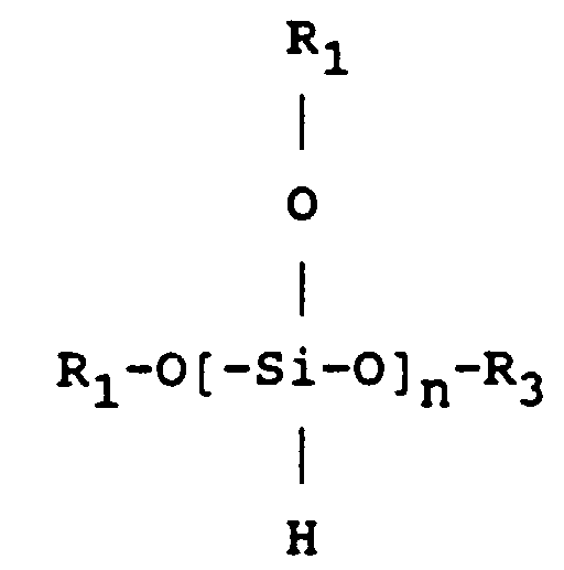
- R1, R2, R3 désignant : CH3, C2H5, C6H6, H, NH2
- un siloxane de formule:

- ou un silazane de formule:

- an alkoxysilane of formula
- R 1 , R 2 , R 3 denoting: CH 3 , C 2 H 5 , C 6 H 6 , H, NH 2
- a siloxane of formula:
- or a silazane of formula:
On a constaté que dans tous les cas la présence d'oxygène introduit dans l'enceinte 5 en même temps que le composé organo-silicé, favorisait considérablement la vitesse de formation de la couche sur le substrat 12.It has been found that in all cases the presence of oxygen introduced into the
Lorsqu'on introduit dans l'enceinte à plasma 5 un alkoxysilane et lorsque la teneur en oxygène introduite dans l'enceinte est inférieure à quelques pour cent, on obtient sur le substrat 12 une couche de silice amorphe.When an alkoxysilane is introduced into the
Lorsqu'on introduit dans l'enceinte à plasma 5 un alkoxysilane et lorsque la teneur en oxygène est supérieure à quelques pour cent, on obtient sur le substrat 12 une couche d'un mélange de silice amorphe et de silice polymérisée.When an alkoxysilane is introduced into the
Par ailleurs, lorsqu'on introduit dans l'enceinte à plasma 5 un siloxane et lorsque la teneur en oxygène introduite dans l'enceinte est inférieure à quelques pour cent, on obtient sur le substrat 12 une couche formée par le mélange des composés suivants:
- polymère (Si-O-Si) réticulé
- -Si-(CH3)1
- -Si-OH
- -Si-NH-Si
- crosslinked polymer (Si-O-Si)
- -Si- (CH3) 1
- -Si-OH
- -Si-NH-Si
Lorsqu'on introduit dans l'enceinte à plasma 5 un siloxane et lorsque la teneur en oxygène introduite dans l'enceinte est supérieure à quelques pour cent, on obtient sur le substrat une couche formée par le mélange des composés suivants:
- polymère (Si-O-Si) réticulé
- -Si-(CH3)2
- -Si-(CH3)3
- -Si-OH
- -Si-NH-Si
- crosslinked polymer (Si-O-Si)
- -Si- (CH3) 2
- -Si- (CH3) 3
- -Si-OH
- -Si-NH-Si
La présence des radicaux -OH, -NH ou -NH2 est importante dans la mesure où elle gouverne les propriétés diélectriques du dépôt.The presence of the radicals -OH, -NH or -NH 2 is important insofar as it governs the dielectric properties of the deposit.
Lorsqu'on introduit dans l'enceinte à plasma 5 un silazane, on obtient sur le substrat 12 une couche formée par le mélange des composés suivants:
- -Si-NH-Si
- -Si-O-Si
- -Si-C-Si
- -Si-NH-Si
- -Si-O-Si
- -If-C-Si
Le substrat peut être métallique, en céramique ou en polymère.The substrate can be metallic, ceramic or polymer.
La couche obtenue peut présenter une épaisseur contrôlée pouvant être comprise entre 500 Å et 50 µm. La vitesse de dépôt de la couche peut être de l'ordre de 1 µm/mn.The layer obtained can have a controlled thickness which can be between 500 Å and 50 µm. The deposition rate of the layer can be of the order of 1 μm / min.
Les substrats revêtus d'une telle couche peuvent être utilisés en tant que composants comportant une couche de passivation pour la protection électrique ou thermique, notamment dans l'électronique embarquée.The substrates coated with such a layer can be used as components comprising a passivation layer for electrical or thermal protection, in particular in on-board electronics.
L'introduction dans le réacteur (5) d'un gaz réactif complémentaire simultanément avec un ou plusieurs des composés organosilicés précités permet de contrôler des propriétés électriques ou diélectriques de la couche mince déposée.The introduction into the reactor (5) of a complementary reactive gas simultaneously with one or more of the above-mentioned organosilicon compounds makes it possible to control the electrical or dielectric properties of the deposited thin layer.
Les gaz introduits sont des ions (anions ou cations comportant des métaux) mis en phase gazeuse sous forme d'halogénures, d'oxhyhalogénures ou de complexes tels des acétylacétonates, des fluoroacétylacétonates,... ou d'autres agents complexants.The gases introduced are ions (anions or cations comprising metals) placed in the gas phase in the form of halides, oxyhyhalides or complexes such as acetylacetonates, fluoroacetylacetonates, etc. or other complexing agents.
On forme ainsi des couches minces composites (polymère céramique) de propriétés électriques ou diélectriques contrôlées.Composite thin layers (ceramic polymer) are thus formed with controlled electrical or dielectric properties.
Claims (14)
- Process for applying a polymeric thin layer onto a metallic, inorganic or organic substrate (12), in which a delayed nitrogen plasma consisting essentially of free nitrogen atoms is produced in a vessel (5) in which the substrate (12) is situated, characterized in that a gaseous organosilicon or -germanium compound containing CH, Si (or Ge), O or NH groups is introduced into the said vessel (5) during the formation of the delayed nitrogen plasma.
- Process in accordance with Claim 1, characterized in that the said gaseous siliceous compound is chosen from alkoxysilanes, siloxanes and silazanes.
- Process in accordance with either of Claims 1 and 2, characterized in that a gaseous compound containing oxygen is added to the gaseous compound introduced into the vessel (5).
- Process in accordance with Claim 3, characterized in that the gaseous compound containing oxygen is molecular oxygen.
- Process in accordance with one of the preceding claims, characterized in that an anion or cation containing a metal, in the form of gaseous compound, is additionally introduced into the plasma vessel.
- Process in accordance with Claim 5, characterized in that the said gaseous compound is chosen from halides, oxyhalides and organometallic compounds such as acetylacetonates and fluoroacetylacetonates.
- Process for deposition of a polymeric thin layer onto a metallic, inorganic or organic substrate (12), the said deposition being performed in a vessel (5) by recombination at the surface of the substrate of the products originating from the dissociation of a precursor gas by a plasma-forming gas originating from a plasma generated in a discharge cavity (3), characterized in that the said plasma is a delayed nitrogen plasma and in that the precursor gas is an organosilicon or organogermanium gas.
- Process according to Claim 7, characterized in that the delayed plasma is a flowing delayed cold plasma.
- Process according to Claim 8, characterized in that the flowing delayed cold plasma consists essentially of free nitrogen atoms.
- Process according to either of Claims 8 and 9, characterized in that the nitrogen pressure is between 1 hPa and 20 hPa.
- Process according to any one of Claims 7 to 10, characterized in that the precursor gas of the deposit is introduced between the exit of the cavity (3) in which the discharge generating the plasma is maintained and the entry of the vessel (5).
- Process according to any one of Claims 7 to 11, characterized in that the organosilicon compound is chosen from the alkoxysilanes of formula:

the siloxanes of formula:
or the siloxanes of formula:
R1, R2 and R3 denoting CH3, C2H5, C6H6, H or NH2. - Process according to any one of Claims 7 to 12, characterized in that oxygen is introduced during the said deposition into the said vessel (5) so as to accelerate the rate of deposition of the polymeric layer.
- Process according to any one of Claims 7 to 13, characterized in that a doping component, chosen from the bodies of chemical formula NH3, NF3, CF4 or SF6, is introduced into the vessel (5).
Applications Claiming Priority (3)
| Application Number | Priority Date | Filing Date | Title |
|---|---|---|---|
| FR9301484A FR2701492B1 (en) | 1993-02-10 | 1993-02-10 | Method for depositing a thin layer on a substrate by cold nitrogen plasma. |
| FR9301484 | 1993-02-10 | ||
| PCT/FR1994/000149 WO1994018355A1 (en) | 1993-02-10 | 1994-02-09 | Method for thin film deposition on a substrate using remote cold nitrogen plasma |
Publications (2)
| Publication Number | Publication Date |
|---|---|
| EP0683825A1 EP0683825A1 (en) | 1995-11-29 |
| EP0683825B1 true EP0683825B1 (en) | 1997-08-13 |
Family
ID=9443921
Family Applications (1)
| Application Number | Title | Priority Date | Filing Date |
|---|---|---|---|
| EP94906936A Expired - Lifetime EP0683825B1 (en) | 1993-02-10 | 1994-02-09 | Method for thin film deposition on a substrate using remote cold nitrogen plasma |
Country Status (9)
| Country | Link |
|---|---|
| EP (1) | EP0683825B1 (en) |
| JP (1) | JPH08506381A (en) |
| KR (1) | KR960701237A (en) |
| AT (1) | ATE156866T1 (en) |
| CA (1) | CA2155659A1 (en) |
| DE (1) | DE69404971T2 (en) |
| FI (1) | FI953779A (en) |
| FR (1) | FR2701492B1 (en) |
| WO (1) | WO1994018355A1 (en) |
Families Citing this family (4)
| Publication number | Priority date | Publication date | Assignee | Title |
|---|---|---|---|---|
| FR2718155B1 (en) * | 1994-04-05 | 1996-04-26 | Europ Composants Electron | Method for depositing a dielectric and / or metal on a substrate. |
| EP0850266B1 (en) * | 1995-09-15 | 2002-06-05 | Tarkett Sommer S.A. | Method for obtaining a floor covering and product thus obtained |
| US7129187B2 (en) * | 2004-07-14 | 2006-10-31 | Tokyo Electron Limited | Low-temperature plasma-enhanced chemical vapor deposition of silicon-nitrogen-containing films |
| US20230054056A1 (en) * | 2019-12-19 | 2023-02-23 | Agc Glass Europe | Silicon oxide coated polymer films and low pressure pecvd methods for producing the same |
Family Cites Families (7)
| Publication number | Priority date | Publication date | Assignee | Title |
|---|---|---|---|---|
| US4363828A (en) * | 1979-12-12 | 1982-12-14 | International Business Machines Corp. | Method for depositing silicon films and related materials by a glow discharge in a disiland or higher order silane gas |
| US4863755A (en) * | 1987-10-16 | 1989-09-05 | The Regents Of The University Of California | Plasma enhanced chemical vapor deposition of thin films of silicon nitride from cyclic organosilicon nitrogen precursors |
| FR2651782B1 (en) * | 1989-09-14 | 1993-03-19 | Air Liquide | PROCESS FOR MAKING A DEPOSIT OF AN INORGANIC AND AMORPHOUS COATING ON AN ORGANIC POLYMERIC SUBSTRATE. |
| US4980196A (en) * | 1990-02-14 | 1990-12-25 | E. I. Du Pont De Nemours And Company | Method of coating steel substrate using low temperature plasma processes and priming |
| FR2661688B1 (en) * | 1990-05-02 | 1992-07-17 | Air Liquide | MULTILAYER COATING FOR POLYCARBONATE SUBSTRATE AND PROCESS FOR PREPARING SUCH A COATING. |
| JPH0782999B2 (en) * | 1991-04-15 | 1995-09-06 | 株式会社半導体プロセス研究所 | Vapor growth film forming method, semiconductor manufacturing apparatus, and semiconductor device |
| DE4126759A1 (en) * | 1991-08-13 | 1993-02-18 | Siemens Ag | Thin, silicon-contg. organic layers prodn. - by irradiation of organo-silane(s)-alkoxy:silane(s) or -siloxane(s) with pulsed laser light of specified wavelength, pulse length, frequency and energy |
-
1993
- 1993-02-10 FR FR9301484A patent/FR2701492B1/en not_active Expired - Fee Related
-
1994
- 1994-02-09 EP EP94906936A patent/EP0683825B1/en not_active Expired - Lifetime
- 1994-02-09 KR KR1019950703277A patent/KR960701237A/en not_active Application Discontinuation
- 1994-02-09 JP JP6517733A patent/JPH08506381A/en active Pending
- 1994-02-09 WO PCT/FR1994/000149 patent/WO1994018355A1/en active IP Right Grant
- 1994-02-09 AT AT94906936T patent/ATE156866T1/en not_active IP Right Cessation
- 1994-02-09 CA CA002155659A patent/CA2155659A1/en not_active Abandoned
- 1994-02-09 DE DE69404971T patent/DE69404971T2/en not_active Expired - Fee Related
-
1995
- 1995-08-09 FI FI953779A patent/FI953779A/en not_active Application Discontinuation
Also Published As
| Publication number | Publication date |
|---|---|
| CA2155659A1 (en) | 1994-08-18 |
| JPH08506381A (en) | 1996-07-09 |
| DE69404971T2 (en) | 1997-12-18 |
| FR2701492A1 (en) | 1994-08-19 |
| FI953779A0 (en) | 1995-08-09 |
| KR960701237A (en) | 1996-02-24 |
| WO1994018355A1 (en) | 1994-08-18 |
| ATE156866T1 (en) | 1997-08-15 |
| FR2701492B1 (en) | 1996-05-10 |
| FI953779A (en) | 1995-09-22 |
| DE69404971D1 (en) | 1997-09-18 |
| EP0683825A1 (en) | 1995-11-29 |
Similar Documents
| Publication | Publication Date | Title |
|---|---|---|
| Rau et al. | Mechanisms of plasma polymerization of various silico-organic monomers | |
| JP6056854B2 (en) | GAS BARRIER FILM, METHOD FOR PRODUCING GAS BARRIER FILM, AND ELECTRONIC DEVICE | |
| US5643838A (en) | Low temperature deposition of silicon oxides for device fabrication | |
| CN1042577C (en) | A method of treating a semi-conductor wafer | |
| BE1019991A3 (en) | METHOD FOR DEPOSITION OF LAYERS ON LOW PRESSURE PECVD GLASS SUBSTRATE. | |
| US4704299A (en) | Process for low temperature curing of sol-gel thin films | |
| US5376591A (en) | Method for manufacturing semiconductor device | |
| EP0115970A1 (en) | Vessel for the processing and particularly etching of substrates by the reactive plasma method | |
| CN102113099B (en) | Silicon precursors to make ultra low-K films with high mechanical properties by plasma enhanced chemical vapor deposition | |
| JPWO2012077553A1 (en) | GAS BARRIER FILM, METHOD FOR PRODUCING GAS BARRIER FILM, AND ELECTRONIC DEVICE | |
| CN1316099A (en) | Method and apparatus for forming film on substrate | |
| Kakiuchi et al. | Silicon oxide coatings with very high rates (> 10 nm/s) by hexamethyldisiloxane-oxygen fed atmospheric-pressure VHF plasma: film-forming behavior using cylindrical rotary electrode | |
| EP0683825B1 (en) | Method for thin film deposition on a substrate using remote cold nitrogen plasma | |
| JPH0512433B2 (en) | ||
| Mascagni et al. | Corrosion resistance of 2024 aluminum alloy coated with plasma deposited aC: H: Si: O films | |
| KR100845941B1 (en) | Manufacturing method of low-k thin films and after annealing processes using rta, low-k thin films manufactured therefrom | |
| WO2009030763A2 (en) | Method for depositing a fluorinated layer from a precursor monomer | |
| Brooks et al. | Plasma-enhanced chemical vapor deposition of silicon nitride from 1, 1, 3, 3, 5, 5-hexamethylcyclotrisilazane and ammonia | |
| WO2006064161A1 (en) | Method and installation for treating a glass substrate incorporating a magnetron line and a device generating an atmospheric pressure plasma | |
| JP4180393B2 (en) | Method for forming low dielectric constant interlayer insulating film | |
| FR2887872A1 (en) | Production of large glass products in combined substrate production and hot atmospheric plasma surface modification installation to confer wide range of functional layers | |
| Francescangeli et al. | Deposition of Barrier Coatings from Vinyltrimethylsilane‐Fed Glow Discharges | |
| US9371430B2 (en) | Porous film with high hardness and a low dielectric constant and preparation method thereof | |
| Yang et al. | Effect of Post-Plasma Treatment Time on the Properties of Low Dielectric Fluorinated Amorphous Carbon Films | |
| CN114703465A (en) | Method for improving adhesion of PECVD (plasma enhanced chemical vapor deposition) fluorocarbon coating on gold surface |
Legal Events
| Date | Code | Title | Description |
|---|---|---|---|
| PUAI | Public reference made under article 153(3) epc to a published international application that has entered the european phase |
Free format text: ORIGINAL CODE: 0009012 |
|
| 17P | Request for examination filed |
Effective date: 19950714 |
|
| AK | Designated contracting states |
Kind code of ref document: A1 Designated state(s): AT BE CH DE ES FR GB IE IT LI LU NL SE |
|
| 17Q | First examination report despatched |
Effective date: 19960124 |
|
| GRAG | Despatch of communication of intention to grant |
Free format text: ORIGINAL CODE: EPIDOS AGRA |
|
| GRAH | Despatch of communication of intention to grant a patent |
Free format text: ORIGINAL CODE: EPIDOS IGRA |
|
| GRAH | Despatch of communication of intention to grant a patent |
Free format text: ORIGINAL CODE: EPIDOS IGRA |
|
| RAP1 | Party data changed (applicant data changed or rights of an application transferred) |
Owner name: THOMSON-CSF PASSIVE COMPONENTS |
|
| GRAA | (expected) grant |
Free format text: ORIGINAL CODE: 0009210 |
|
| AK | Designated contracting states |
Kind code of ref document: B1 Designated state(s): AT BE CH DE ES FR GB IE IT LI LU NL SE |
|
| PG25 | Lapsed in a contracting state [announced via postgrant information from national office to epo] |
Ref country code: NL Free format text: LAPSE BECAUSE OF FAILURE TO SUBMIT A TRANSLATION OF THE DESCRIPTION OR TO PAY THE FEE WITHIN THE PRESCRIBED TIME-LIMIT Effective date: 19970813 Ref country code: ES Free format text: THE PATENT HAS BEEN ANNULLED BY A DECISION OF A NATIONAL AUTHORITY Effective date: 19970813 Ref country code: AT Effective date: 19970813 |
|
| REF | Corresponds to: |
Ref document number: 156866 Country of ref document: AT Date of ref document: 19970815 Kind code of ref document: T |
|
| REG | Reference to a national code |
Ref country code: CH Ref legal event code: EP |
|
| ITF | It: translation for a ep patent filed | ||
| REF | Corresponds to: |
Ref document number: 69404971 Country of ref document: DE Date of ref document: 19970918 |
|
| GBT | Gb: translation of ep patent filed (gb section 77(6)(a)/1977) |
Effective date: 19970905 |
|
| PG25 | Lapsed in a contracting state [announced via postgrant information from national office to epo] |
Ref country code: SE Effective date: 19971113 |
|
| NLV1 | Nl: lapsed or annulled due to failure to fulfill the requirements of art. 29p and 29m of the patents act | ||
| PG25 | Lapsed in a contracting state [announced via postgrant information from national office to epo] |
Ref country code: LU Free format text: LAPSE BECAUSE OF NON-PAYMENT OF DUE FEES Effective date: 19980209 |
|
| PG25 | Lapsed in a contracting state [announced via postgrant information from national office to epo] |
Ref country code: LI Free format text: LAPSE BECAUSE OF NON-PAYMENT OF DUE FEES Effective date: 19980228 Ref country code: CH Free format text: LAPSE BECAUSE OF NON-PAYMENT OF DUE FEES Effective date: 19980228 |
|
| PG25 | Lapsed in a contracting state [announced via postgrant information from national office to epo] |
Ref country code: IE Free format text: LAPSE BECAUSE OF NON-PAYMENT OF DUE FEES Effective date: 19980605 |
|
| PLBE | No opposition filed within time limit |
Free format text: ORIGINAL CODE: 0009261 |
|
| STAA | Information on the status of an ep patent application or granted ep patent |
Free format text: STATUS: NO OPPOSITION FILED WITHIN TIME LIMIT |
|
| REG | Reference to a national code |
Ref country code: IE Ref legal event code: FD4D Ref document number: 75851 Country of ref document: IE |
|
| 26N | No opposition filed | ||
| REG | Reference to a national code |
Ref country code: CH Ref legal event code: PL |
|
| REG | Reference to a national code |
Ref country code: GB Ref legal event code: IF02 |
|
| PGFP | Annual fee paid to national office [announced via postgrant information from national office to epo] |
Ref country code: DE Payment date: 20020122 Year of fee payment: 9 |
|
| PGFP | Annual fee paid to national office [announced via postgrant information from national office to epo] |
Ref country code: GB Payment date: 20020124 Year of fee payment: 9 |
|
| PGFP | Annual fee paid to national office [announced via postgrant information from national office to epo] |
Ref country code: FR Payment date: 20020208 Year of fee payment: 9 |
|
| PGFP | Annual fee paid to national office [announced via postgrant information from national office to epo] |
Ref country code: BE Payment date: 20020318 Year of fee payment: 9 |
|
| PG25 | Lapsed in a contracting state [announced via postgrant information from national office to epo] |
Ref country code: GB Free format text: LAPSE BECAUSE OF NON-PAYMENT OF DUE FEES Effective date: 20030209 |
|
| PG25 | Lapsed in a contracting state [announced via postgrant information from national office to epo] |
Ref country code: BE Free format text: LAPSE BECAUSE OF NON-PAYMENT OF DUE FEES Effective date: 20030228 |
|
| PG25 | Lapsed in a contracting state [announced via postgrant information from national office to epo] |
Ref country code: DE Free format text: LAPSE BECAUSE OF NON-PAYMENT OF DUE FEES Effective date: 20030902 |
|
| GBPC | Gb: european patent ceased through non-payment of renewal fee | ||
| PG25 | Lapsed in a contracting state [announced via postgrant information from national office to epo] |
Ref country code: FR Free format text: LAPSE BECAUSE OF NON-PAYMENT OF DUE FEES Effective date: 20031031 |
|
| REG | Reference to a national code |
Ref country code: FR Ref legal event code: ST |
|
| PG25 | Lapsed in a contracting state [announced via postgrant information from national office to epo] |
Ref country code: IT Free format text: LAPSE BECAUSE OF NON-PAYMENT OF DUE FEES;WARNING: LAPSES OF ITALIAN PATENTS WITH EFFECTIVE DATE BEFORE 2007 MAY HAVE OCCURRED AT ANY TIME BEFORE 2007. THE CORRECT EFFECTIVE DATE MAY BE DIFFERENT FROM THE ONE RECORDED. Effective date: 20050209 |