EP0675500B1 - An improved memory device and method of construction - Google Patents
An improved memory device and method of construction Download PDFInfo
- Publication number
- EP0675500B1 EP0675500B1 EP95104520A EP95104520A EP0675500B1 EP 0675500 B1 EP0675500 B1 EP 0675500B1 EP 95104520 A EP95104520 A EP 95104520A EP 95104520 A EP95104520 A EP 95104520A EP 0675500 B1 EP0675500 B1 EP 0675500B1
- Authority
- EP
- European Patent Office
- Prior art keywords
- latch
- memory
- address
- block
- output
- Prior art date
- Legal status (The legal status is an assumption and is not a legal conclusion. Google has not performed a legal analysis and makes no representation as to the accuracy of the status listed.)
- Expired - Lifetime
Links
Images

Classifications
-
- G—PHYSICS
- G11—INFORMATION STORAGE
- G11C—STATIC STORES
- G11C7/00—Arrangements for writing information into, or reading information out from, a digital store
- G11C7/10—Input/output [I/O] data interface arrangements, e.g. I/O data control circuits, I/O data buffers
- G11C7/1051—Data output circuits, e.g. read-out amplifiers, data output buffers, data output registers, data output level conversion circuits
- G11C7/106—Data output latches
-
- G—PHYSICS
- G11—INFORMATION STORAGE
- G11C—STATIC STORES
- G11C7/00—Arrangements for writing information into, or reading information out from, a digital store
- G11C7/10—Input/output [I/O] data interface arrangements, e.g. I/O data control circuits, I/O data buffers
- G11C7/1051—Data output circuits, e.g. read-out amplifiers, data output buffers, data output registers, data output level conversion circuits
Definitions
- Memory devices including SRAM's, DRAM's and ROM's are widely used in electronic circuits to store data in the form of logic bits which can be accessed by using a memory address.
- a memory address is provided to a memory device, and the memory device executes a memory cycle to provide data from or store data to the location in the memory device associated with the memory address.
- a memory write cycle usually operates in a manner similar to a memory read cycle with the data state of the memory cell corresponding to the memory address being set according to a data value provided to the memory device.
- Memory devices can be designed such that read and write cycles can read from or store to one or more memory cells.
- address transition detection is used to detect changes in the memory address and to initiate a full memory cycle only when the memory address changes sufficiently.
- a low power access mode can be implemented by distinguishing row address changes from column address changes and initiating a memory array access only when the row address changes.
- One implementation of such a low power access mode is to latch the outputs of the memory array representing the data states of memory cells corresponding to the row address.
- a change in the memory address that only includes a change in the column address then can be handled by accessing the latched data states rather than accessing the memory array.
- This low power access mode saves power by preventing the memory device from precharging the memory array and decoding the full memory address for memory read cycles during which the row address does not change.
- the sensing of the outputs of the memory array consumes power and can cause a power consumption problem in memory devices with large memory arrays. Sensing the outputs of the memory array prior to multiplexing the outputs can require the driving of column lines and activating sense amplifiers equal to the width of the memory array. For example, a 64k-bit RAM having 256 rows and 256 columns would require 256 sense amplifiers to sense the data states of every memory cell in one row. Even in a memory access cycle in which the row address does not change, the 256 columns must be driven and 256 sense amplifiers activated consuming power. Further, if the outputs of the memory array are implemented as differential signals and are multiplexed, sense amplifiers must be paired with each input to the multiplexer and also consume power. Driving these devices causes power consumption even during a low power access mode when the row address does not change. This power consumption is a problem because it is desirable for a memory device to consume as little power as possible.
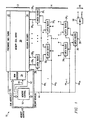
- FIGURE 1 illustrates a block diagram of a memory device indicated generally at 10 constructed according to the teachings of the present invention.
- Memory device 10 comprises a memory array indicated generally at 12, a multiplexer block indicated generally at 14, a memory control block 16, and an output block indicated generally at 18.
- a MEMORY ADDRESS comprising a ROW ADDRESS and a COLUMN ADDRESS is provided to memory control block 16 and to memory array 12 as shown.
- Latch block 30 1 through latch block 30 i comprise a first stage of multiplexer block 14.
- Latch block 30 1 is coupled to memory array outputs 28 1 and 28 2 .
- Latch block 30 1 is coupled to the last two memory array outputs 28 n-1 and 28 n .
- the first stage of latch blocks comprises a number of latch blocks equal to i.
- the number of latch blocks in the first stage can be any suitable number coupled to receive all of the memory array outputs 28 1 through 28 n .
- a second stage of latch blocks comprises latch block 32 1 through latch block 32 j .
- the number of latch blocks j in the second stage depends upon the number of inputs to each of the j latch blocks in the second stage. In the embodiment shown in FIGURE 1, each latch block receives two outputs from the prior stage. Therefore, the number of latch blocks j in the second stage is equal to one-half the number of latch blocks i in the first stage.
- Multiplexer block 14 can comprise any suitable number of stages of latch blocks.
- all of the latch blocks in multiplexer block 14 receive two inputs and provide one output and multiplexer block 14 comprises m stages.
- the latch blocks each receive three or more of the memory array outputs 28 1 through 28 n of the memory array 12.
- each of the latch blocks have the same number of inputs.
- latching and non-latching multiplexer elements may be intermixed.
- the sequential numbering of the inputs does not imply that the inputs come from any particular ordering of the outputs from the previous stage or columns of the memory array 12.
- Memory control block 16 provides memory control signals 40, 41, and 42 and provides multiplexer control signals 44.
- Memory control signal 40 is coupled to the precharge and timing circuit 22.
- Memory control signal 41 is coupled to the row decoder 24, and memory control signal 42 is coupled to column decoder 26.
- Multiplexer control signals 44 comprise multiplexer control signals for each stage of multiplexer block 14. As shown in FIGURE 1, multiplexer control signals 44 comprise multiplexer control signals 44 1 through multiplexer control signals 44 m.
- Multiplexer control signals 44 1 are coupled to latch blocks 30 1 through latch blocks 30 i in the first stage, and multiplexer control signals 442 are coupled to latch blocks 32 1 through 32 j in the second stage as shown.
- Multiplexer control signals 44 m-1 are coupled to latch blocks 34 1 and 34 2 , and multiplexer control signals 44 m are coupled to latch block 36 as shown.
- memory array outputs 28 1 through 28 n are differential signals, and the outputs of each latch block in multiplexer block 14 are differential si gnals. Differential signals may be used for all or a subset of the latch block outputs.
- Output block 18 comprises an input/output buffer 50.
- Input/output buffer 50 is coupled to multiplexer block output 38 and to an input data bit D.
- the input/output buffer 50 provides an output data bit Q.
- separate input and output paths may be used.
- Some memories are organized so that a common input/output (I/O) pin is used for input and output of data.
- the buffer is referred to as an input/output (I/O) buffer.
- I/O input/output
- separate pins are used for input and output of data.
- common busses may or may not be used for the multiplexing and transfer of data from the memory array to the buffer and from the buffer to the memory array.
- separate circuitry generally is used for driving the busses for input data and for output data.
- the teachings of the present invention relate to the multiplexing of the output data, and are applicable whether or not common I/O busses and/or common I/O buffers are used.
- Memory device 10 operates to provide a data state of a memory cell corresponding to the MEMORY ADDRESS as data output Q and operates to store data input D by setting a data state of a memory cell corresponding to the MEMORY ADDRESS.
- Memory array 12 operates to provide data states of memory cells in a row of memory cell array 20 corresponding to the ROW ADDRESS.
- the ROW ADDRESS and the COLUMN ADDRESS are provided to row decoder 24 and to column decoder 26, as shown.
- Memory array 12 provides the data states of the memory cells in memory cell array 20 corresponding to the ROW ADDRESS and the COLUMN ADDRESS responsive to the row decoder 24 and the column decoder 26.
- Memory array 12 is operable to provide all or a subset of the data states of the memory cells in the indicated row of memory cell array 20 as memory array outputs 28 1 through 28 n . In the illustrated embodiment of the present invention, memory array 12 provides n memory array outputs 28 1 through 28 n .
- Memory control block 16 operates to generate memory control signals 40, 41, and 42. Memory control block 16 controls precharge and timing circuit 22 with memory control signal 40. Memory control block 16 controls row decoder 24 and column decoder 26 with memory control signal 41 and memory control signal 42, respectively. Memory control block 16 operates to generate multiplexer control signals 44 comprising multiplexer control signals 44 1 through 44 m . Memory control block 16 controls operation of each stage in multiplexer block 14 with multiplexer control signals 44 1 through 44 m .
- Multiplexer block 14 operates to multiplex memory array outputs 28 1 through 28 n to provide multiplexer block output 38.
- Multiplexer block output 38 represents the data state of the memory cell corresponding to the MEMORY ADDRESS provided to memory device 10.
- multiplexer block 14 can comprise a number of latch blocks arranged in a number of stages. The latch blocks are arranged such that memory array outputs 28 1 through 28 n are multiplexed to set multiplexer block output 38.
- One of memory array outputs 28 1 through 28 n represents the data state of the memory cell corresponding to the MEMORY ADDRESS.
- Multiplexer block 14 operates to select the appropriate data state and provide that data state as multiplexer block output 38.
- Multiplexer block 14 operates to multiplex data states from the number of memory array outputs provided by memory array 12 to set multiplexer block output 38 provided to output block 18.
- the number of output data bits can be any suitable number and is shown as one bit for illustrative purposes only. One alternative is a multiple bit output with parallel output paths.
- Each latch block comprises at least one input and an output.
- the number of inputs relates to the degree of multiplexing to be accomplished at a given stage. If there is only one input, the latch block acts as a relay.
- each latch block comprises two inputs because multiplexing by a factor of two is to be accomplished at each stage.
- the latch block is operable to latch its output.
- FIGURE 2a where each latch block comprises one latch and at least one input, with a sense amplifier associated with each input.
- the latch block is operable to latch each input.
- FIGURE 2c where the latch block comprises a sense amplifier and a latch associated with each input.
- the latch block is operable to multiplex the inputs and provide an output.
- the latch block is further operable to provide an output from latched data.
- multiplexer block 14 The operation of multiplexer block 14 is controlled by multiplexer control signals 44 provided by memory control block 16. Multiplexer control signals 44 1 through 44 m control the operation of the latch cells in the latch blocks in multiplexer block 14.
- One embodiment for controlling the latch blocks is for the multiplexer control signals 44 to operate to control the latch blocks such that each latch cell latches a data state only if the input to the latch cell corresponds to the COLUMN ADDRESS.
- the multiplexer control signals 44 operate to control the latch blocks such that each latch cell always latches the data state of the input to the latch cell.
- Multiplexer control signals 44 1 through 44 m control the output of each latch block in multiplexer stage 14 and the latching of data states by the latch cells.
- multiplexer block 14 also is operable to connect input/output buffer 50 to memory array 12 allowing a data input bit to be stored as a data state of a memory cell in memory cell array 20.
- memory control block 16 controls the latch blocks in the multiplexer block 14 such that an appropriate one of memory array outputs 28 1 through 28 n is set to the data state of input data bit D.
- the input data may also be latched at the intermediate multiplex latches and and become available for subsequent output from these latches.
- a technical advantage of the present invention is latching of data states in multiplexer block 14. Space can be limited when a memory device is constructed in an integrated circuit on a semiconductor chip.
- the number of latch blocks and number of stages in multiplexer block 14 can be designed as suitable for the space available.
- Some conventional memory devices have a sense amplifier and a latch at each column. This may be difficult to fit in the pitch of the memory array.
- any number of columns may be multiplexed into the first latch block. This initial multiplexing before the first latch block may be done in a single or multiple stages of multiplexing.
- Latches may be implemented at desired levels of multiplexing. Latches alternatively may be implemented only at the first stage of multiplexing, only at the last stage of multiplexing, only at an intermediate stage of multiplexing, or at any selected subset of the stages of multiplexing.
- the likelihood of accessing data that is in a latch will be high if the address sequencing and the multiplexing are arranged so that the information stored in the latches are for sequential addresses. This is true even with only a few latches such as latches only in the last stage of multiplexing.
- one embodiment of the present invention is to have the addresses of the latches defined by the least significant, or most frequently changed, bits in the memory address.
- a 64K memory could be arranged in 256 rows and 256 columns, with address bits a0-a7 specifying the column and address bits a8-a15 specifying the row.
- the columns can be multiplexed in three stages, going from 256 bits to 32 bits to 4 bits to the final one bit output. If latches are placed at the 4 bit stage of the multiplexer and the address bits a0 and a1 specify the location among those four bits, then there will be the greatest saving in power if address bits a0 and a1 are the most frequently changed.
- latches are included only at the 32 bit stage of the multiplexing, and address bits a0 through a4 specify these locations, then there will be power savings when the address changes only in bits a0 through a4 in successive cycles. In this second case, the power savings will not be as great for one such cycle as it would be if the latch were at the last stage of multiplexing, as in the first case, but the low power mode spans a greater address space. Latches could be placed at both stages of the multiplexer to gain the benefits of both cases, a low power mode for a wider address space, and the lowest power for a segment of that address space, at some cost in circuitry complexity and area.
- the present invention teaches a memory device architecture having latches at the multiplexer block 14 reducing power consumption. Power consumption is reduced whether or not differential signals are implemented although the power savings is greater when differential signals are used in the multiplexer block 14.
- the memory device architecture of the present invention is beneficial for all memories, but is especially beneficial for memories implemented using large cell arrays.
- a technical advantage of the present invention is the use of latches with differential signals in the multiplexer block 14.
- Use of differential signals can reduce the delay in propagating a signal through the multiplexer block, particularly for large memories, by eliminating the need for full signal swings on the busses.
- the reduced signal swing can also reduce power, but the holding and sensing of differential signals generally consumes significant power.
- the use of latches to reduce the number of occurrences requiring the driving and sensing of differential signals saves significant power.
- a further technical advantage of the present invention is latching the differential signals without driving the differential signals from rail to rail.
- the use of latches can conflict with the use of differential signals because latches often are full signal.
- the latch cells in multiplexer block 14 are constructed such that the differential signals are not driven from rail to rail.
- One embodiment of a latch cell is illustrated in FIGURES 2a and 2b. The latches in the latch cells are driven from rail to rail, but the differential signals are only driven with a differential swing.
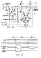
- FIGURE 2a illustrates one embodiment of a latch cell indicated generally at 60 constructed according to the teachings of the present invention.
- Latch cell 60 comprises a sense amplifier 62 and a latch 73.
- Sense amplifier 62 comprises an n-channel field effect transistor (N-FET) 63 and an N-FET 64.
- a gate of N-FET 63 is coupled to a line 65, and a gate of N-FET 64 is coupled to a line 66.
- a drain of N-FET 63 is coupled to a line 67 and a drain of N-FET 64 is coupled to a line 68.
- a source of N-FET 63 and a source of N-FET 64 are coupled to a NODE 1.
- Sense amplifier 62 further comprises an N-FET 70 and an N-FET 72.
- N-FET 70 comprises a source, a drain coupled to NODE 1, and a gate coupled to a sense amplifier address signal SA ADDRESS.
- N-FET 72 comprises a drain coupled to the source of N-FET 70, a gate coupled to a sense amplifier control signal SA CONTROL and a source coupled to ground potential.
- Latch 73 comprises a p-channel field effect transistor (P-FET) 74 and a PFET 76.
- P-FET 74 comprises a source coupled to line 68, a gate coupled to a second latch control signal LATCH CONTROL 2 and a drain coupled to a NODE 2.
- P-FET 76 comprises a source coupled to line 67, a gate coupled to the second latch control signal LATCH CONTROL 2 and a drain coupled to a NODE 3.
- Latch 73 also comprises a P-FET 78, an N-FET 80, a P-FET 82 and an N-FET 84.
- P-FET 78 comprises a source coupled to a positive power supply V DD , a gate coupled to a NODE 3, and a drain coupled to NODE 2.
- N-FET 80 comprises a drain coupled to NODE 2, a gate coupled to NODE 3, and a source coupled to a NODE 4.
- P-FET 82 comprises a source coupled to positive power supply V DD , a gate coupled to NODE 2, and a drain coupled to NODE 3.
- N-FET 84 comprises a drain coupled to NODE 3, a gate coupled to NODE 2, and a source coupled to NODE 4.
- Latch 73 further comprises an N-FET 86.
- N-FET 86 comprises a drain coupled to NODE 4, a gate coupled to a first latch control signal LATCH CONTROL 1 and a source coupled to ground potential.
- Latch cell 60 further comprises a P-FET 88 and a P-FET 90.
- P-FET 88 comprises a source coupled to power supply V DD , a gate coupled to line 68, and a drain coupled to line 68.
- P-FET 90 comprises a source coupled power supply V DD , a gate coupled to line 67, and a drain coupled to line 67.
- a differential input signal DIFFERENTIAL SIGNAL IN is coupled to line 65 and line 66 and a differential output signal DIFFERENTIAL SIGNAL OUT is coupled to line 67 and line 68.
- Sense amplifier 62 is activated when N-FET 70 and N-FET 72 are turned on by sense amplifier address signal SA ADDRESS and sense amplifier control signal SA CONTROL. When activated, sense amplifier 62 pulls lines 67 and 68 according to the differential on lines 65 and 66.
- Latch 73 is activated when N-FET 86 is turned on by the first latch control signal LATCH CONTROL 1.
- Latch 73 is connected to lines 67 and line 68 when P-FET 74 and P-FET 76 are activated by the second latch control signal LATCH CONTROL SIGNAL 2.
- latch 73 senses and stores the data state of the differential on line 67 and line 68.
- Latch 73 operates to retain a data state when activated and not connected to line 67 and line 68.
- latch 73 operates to drive line 67 and line 68 according to the data state retained in latch 73.
- Latch 73 operates to drive NODE 2 and NODE 3 to the rails, V DD and ground potential, according to the data state of the latch 73. However, lines 67 and 68 are not driven to the rails when latch 73 is connected due to the pull-up operation of P-FET 88 and P-FET 90.
- FIGURE 2a there is one latch on a differential output bus associated with one or more inputs to each latch block.
- FIGURE 2a shows only one of a plurality of possible differential inputs and associated sense amplifiers. The number of inputs determines the degree of multiplexing at this stage. With one input, this would act as a relay stage without multiplexing.
- the sense amplifier address signal SA ADDRESS is the signal that selects an input.
- the sense amplifier control signal SA CONTROL activates propagation of the selected input.
- the first latch control signal LATCH CONTROL 1 controls whether or not the latch is latched or unlatched.
- the second latch control signal LATCH CONTROL 2 controls whether or not the latch is connected to the output bus. Variations on sense amplifier and latch design can be used.
- the SA ADDRESS and SA CONTROL signals could be combined by an AND circuit.
- precharge or equalization circuits could be added to the sense amplifier or the latch, with additional control signals for the timing of the precharge/equalization.
- each latch block has one or more sense amplifiers 62 associated with the DIFFERENTIAL SIGNAL OUT and latch 73.
- the sense amplifier signal SA ADDRESS is different for each sense amplifier in a latch block while the sense amplifier control signal SA CONTROL is the same.
- the same set of sense amplifier address signals and sense amplifier control signal is applied in parallel to a parallel configuration of latch blocks, such as latch blocks 30 1 through 30 i in FIGURE 1, and a different set of sense amplifier address signals and sense amplifier control signal are applied to other sets of latch blocks.
- i bits of data are latched although only a subset may be selected for output.
- the latched data is then available for output in subsequent access cycles without activation of the sense amplifiers in that set of parallel latch blocks.
- the latch cell 60 illustrated in FIGURE 2a is one embodiment. Other embodiments of latch cells are possible which would operate according to the teachings of the present invention to drive the differential output signal to match the data state of either the latched value or the differential input signal responsive to control signals. For example, there are many varieties of sense amplifiers that could be used. Also as mentioned above, it is possible to add precharge or equalization circuitry to the sense amplifiers or latches.
- FIGURE 2b illustrates a timing diagram showing one embodiment of the operation of the control signals for the latch cell 60 illustrated in FIGURE 2a.
- the timing diagram of FIGURE 2b illustrates an address bit A n and an address bit A m .
- FIGURE 2b also illustrates the sense amplifier address signal SA ADDRESS, the sense amplifier control signal SA CONTROL, the first latch control signal LATCH CONTROL 1, and the second latch control signal LATCH CONTROL 2.
- the timing diagram of FIGURE 2b comprises three regions indicated 94, 96 and 98 as shown.
- FIGURE 2b illustrates one embodiment in which the control signals are generated from address transition detection applied to selected portions of the memory address.
- Sense amplifier control signal SA CONTROL can enable the sense amplifier when there is a transition in the address associated with data upstream from the sense amplifier.
- the sense amplifier control signal can be generated by standard address transition detection circuitry applied to a subset of the address bits, or by other circuitry such as circuitry to compare a newly input address to a stored address. For the case in which address bits are labeled such that higher address bits are associated with multiplex branches further upstream, including row addresses, this can be expressed as a transition in address bits A n where n is greater than i where i is the highest bit associated with this branch output.
- LATCH CONTROL 1 and LATCH CONTROL 2 are also generated from such an address transition, with timing such that the newly address data is latched.
- a pulse in LATCH CONTROL 2 is also generated by a transition in address bits associated with selection of multiplex branches from this branch to the next latch or to the output if there is no down stream latch. If the memory device is associated with a processor, the processor could generate the control signals. In this case, a plurality of latches could be associated with the differential output bus, and data from different access cycles could be stored in different latches.
- the sense amplifier control signal SA CONTROL is low.
- the first and second latch control signals LATCH CONTROL 1 and LATCH CONTROL 2 are high. Thus, the sense amplifier 62 and latch 73 are not activated.
- the sense amplifier control signal SA CONTROL pulses high. Accordingly, sense amplifier 62 is activated and senses the input signal if the sense amplifier address signal SA ADDRESS is high.
- the first and second latch control signals LATCH CONTROL 1 and LATCH CONTROL 2 pulse high one after the other as shown. New data is latched by the latch 73. These pulses are generated by the transition in A n from region 94 to region 96.
- the second latch control signal LATCH CONTROL 2 pulses low and the sense amplifier control signal SA CONTROL is low.
- the data state held by latch 73 is output on the differential output signal.
- control signals for latch cell 60 can be generated. They can be generated and provided to the memory device by a processor accessing data from the memory. They can be generated by the memory device in response to clock signals and address sequences.
- the memory device can store addresses relating to the data stored in the latches and compare input addresses to the stored addresses.
- the memory device generates the control signals by detecting address bit transitions in selected subsets of the address.
- the sense amplifier control signal SA CONTROL can be generated based on a transition in the address bits relating to the address upstream from the latch, including row address bits.
- the sense amplifier address signal SA ADDRESS can be generated based on a transition in address bits relating to the address at the latch and down stream from the latch.
- Systems can be designed to benefit from this technical advantage of the present invention, for example, when loading a cache memory from a memory device constructed according to the teachings of the present invention.
- the timing of the sense amplifier address signal SA ADDRESS can be delayed so that the output data from the previous access will be valid longer into the current access cycle.
- the timing of control signals SA ADDRESS AND SA CONTROL can be made such that the activation of the sensing, latch, and output are appropriate for a full cycle whether or not a full cycle is activated.
- FIGURE 2c illustrates another embodiment of a latch cell indicated generally at 60 constructed according to the teachings of the present invention.
- the configuration of latch cell 60 of FIGURE 2c is the same as that of FIGURE 2a except for the addition of a P-FET 100, a P-FET 102 and a third latch control signal LATCH CONTROL 3.
- P-FETs 100 and 102 comprise sources coupled to the differential input lines 65 and 66 respectively, gates coupled to the third latch control signal LATCH CONTROL 3, and drains coupled to NODE 2 and NODE 3, respectively, as shown.
- Latch cell 60 can be connected to similarly constructed latch cells to form latch blocks comprised of a plurality of latch cells by connecting the differential output signal DIFFERENTIAL SIGNAL OUT, lines 67 and 68, of each latch cell.
- the plurality of latch cells in a latch block share a differential output signal bus with each latch cell coupled to a different differential input signal.
- PFETs 88 and 90 may be common among the latch cells in the latch block.
- the sense amplifier address signal SA ADDRESS is different for each latch cell in a latch block while the sense amplifier control signal SA CONTROL is the same.
- the latch 73 is associated with a single input to the multiplex branch. Multiple inputs to the branch can be latched simultaneously, even though only one is output. Again, other sense amplifier or latch circuits could be substituted, including the addition of precharge or equalization circuitry.
- the control signals are similar to those in FIGURE 2a, except that LATCH CONTROL 2 controls connection of the latch 73 to the input rather than to the output, and an additional control signal, LATCH CONTROL 3 controls connection to the output.
- FIGURE 2d illustrates a timing diagram showing one embodiment of the operation of the control signals for the latch cell 60 illustrated in FIGURE 2c.
- FIGURE 2d illustrates the same control signals as FIGURE 2b with the addition of the third latch control signal LATCH CONTROL SIGNAL 3.
- FIGURE 2d illustrates the generation of these control signals in response to address bit transitions for one embodiment of the present invention.
- latch cell 60 illustrated in FIGURE 2a is somewhat simpler than the embodiment illustrated in FIGURE 2c, but is also somewhat less effective in lowering the activation of circuit elements when data is accessed from the latch and reducing power consumption.
- a multiplexer comprising two stages.
- Implementing the embodiment of FIGURE 2a in the first of the two stages is somewhat equivalent to implementing the embodiment of FIGURE 2c in the second of the two stages in that the same number of latches would be required.
- the first implementation would require the activation of more circuitry than would the second implementation.
- Other variations and combinations of latches and sense amplifiers are possible according to the teachings of the present invention.
- FIGURE 3 illustrates a block diagram of a computer system indicated generally at 100 utilizing a memory device constructed according to the teachings of the present invention.
- Computer system 100 comprises a processor 102 coupled to a memory device 104.
- Processor 102 comprises a cache memory 105.
- Memory device 104 is constructed according to the teachings of the present invention and includes a multiplexer block comprising an arrangement of latch blocks.
- a disk 106, a keyboard 108 and a display 110 are coupled to processor 102 as shown.
- Processor 102 and memory device 104 operate to allow processor 102 to send a memory address to memory device 104 and to allow memory device 104 either to store data from or return data to processor 102.
- Processor 102 may include a cache memory 105 as shown.
- Disk 106 operates to provide magnetic storage for data provided by processor 102. Disk 106 also operates to provide data to processor 102. Keyboard 108 provides input to the processor 102, and display 110 displays data provided by processor 102.
- the computer system 100 could comprise a number of other elements conventionally used in computer systems. Any computer system utilizing memory devices can benefit from the use of a memory device constructed according to the teachings of the present invention. A large benefit will be derived by having the system map the address bits such that there are sequences of memory accesses in which only a subset of the address bits change, and such that this subset of address bits correspond to the address of the latches in the multiplexer.
Landscapes
- Static Random-Access Memory (AREA)
- Dram (AREA)
- Read Only Memory (AREA)
Description
- This invention relates in general to the field of electronic systems, and more particularly to an improved memory device and method of construction.
- Memory devices including SRAM's, DRAM's and ROM's are widely used in electronic circuits to store data in the form of logic bits which can be accessed by using a memory address. Generally, a memory address is provided to a memory device, and the memory device executes a memory cycle to provide data from or store data to the location in the memory device associated with the memory address.
- Memory devices are implemented according to various architectures. Memory devices may include a memory array containing a large number of memory cells where each memory cell can be set to one of two data states storing one bit of information. The memory cells often are arranged in rows and columns, thus each memory cell can be referenced by a unique memory address which includes a row address and a column address. Generally, a row address selects a word line that enables access of each memory cell in that row to associated column or bit lines, where the bit lines may be in pairs to transmit differential signals. Large memories may be divided into blocks such that the row address selects a global word line that is selectively connected to block word lines in response to the block address. The block address may be included in the general term of column address, since it is part of the address that selects a particular column.
- Memory devices commonly operate in a read mode and a write mode, thus memory devices execute memory read cycles and memory write cycles. In many memory devices, the data states of every memory cell in the row specified by the row address are accessed during a memory read cycle. These data states are then multiplexed according to the column address to provide an output which represents the data states of the memory cells corresponding to the memory address. The number of memory cells for which the data state is output in one access depends on the organization of the given memory. Typical organizations are x1, x4, or x8. The output from a memory array prior to multiplexing represents all or a subset of the memory cells corresponding to the row address. A memory write cycle usually operates in a manner similar to a memory read cycle with the data state of the memory cell corresponding to the memory address being set according to a data value provided to the memory device. Memory devices can be designed such that read and write cycles can read from or store to one or more memory cells.
- In some memory devices, address transition detection is used to detect changes in the memory address and to initiate a full memory cycle only when the memory address changes sufficiently. A low power access mode can be implemented by distinguishing row address changes from column address changes and initiating a memory array access only when the row address changes. One implementation of such a low power access mode is to latch the outputs of the memory array representing the data states of memory cells corresponding to the row address. A change in the memory address that only includes a change in the column address then can be handled by accessing the latched data states rather than accessing the memory array. This low power access mode saves power by preventing the memory device from precharging the memory array and decoding the full memory address for memory read cycles during which the row address does not change.
- While latching the data at each column allows this low power access mode, it may be difficult to layout a latch to fit in the pitch of a column. Also, in large memories, the multiplexing of data from the columns to the output may be done in several stages. The driving and sensing of data through the plurality of stages in the multiplexer further consumes power even in such a low power access mode. This particularly may be true if differential signals are used in multiplexing to reduce access time.
- The sensing of the outputs of the memory array consumes power and can cause a power consumption problem in memory devices with large memory arrays. Sensing the outputs of the memory array prior to multiplexing the outputs can require the driving of column lines and activating sense amplifiers equal to the width of the memory array. For example, a 64k-bit RAM having 256 rows and 256 columns would require 256 sense amplifiers to sense the data states of every memory cell in one row. Even in a memory access cycle in which the row address does not change, the 256 columns must be driven and 256 sense amplifiers activated consuming power. Further, if the outputs of the memory array are implemented as differential signals and are multiplexed, sense amplifiers must be paired with each input to the multiplexer and also consume power. Driving these devices causes power consumption even during a low power access mode when the row address does not change. This power consumption is a problem because it is desirable for a memory device to consume as little power as possible.
- EP-A-0 202 912 discloses a semiconductor memory device (DRAM) comprising a plurality of memory cells arranged in rows and columns, wherein a multiplexer inform of a shift register comprising one stage of latches is coupled to an output of said memory device at each of the columns of said memory cells and sequences through a series of data bits.
- Therefore, a need has arisen for an improved memory device that provides low power consumption.
- In accordance with the present invention, a memory device is provided that substantially eliminates or reduces disadvantages and problems associated with prior memory devices.
- The invention is specified by
claims - A more complete understanding of the present invention and advantages thereof, may be acquired by referring to the following description taken in conjunction with the accompanying drawings in which like reference numbers indicate like features and wherein:
- FIGURE 1 illustrates a block diagram of a memory device constructed according to the teachings of the present invention;
- FIGURE 2a illustrates one embodiment of a latch cell constructed according to the teachings of the present invention;
- FIGURE 2b illustrates a timing diagram showing one embodiment of the operation of the control signals for the latch cell illustrated in FIGURE 2a;
- FIGURE 2c illustrates another embodiment of a latch cell constructed according to the teachings of the present invention;
- FIGURE 2d illustrates a timing diagram showing one embodiment of the operation of the control signals for the latch cell illustrated in FIGURE 2c; and
- FIGURE 3 illustrates a computer system utilizing a memory device constructed according to the teachings of the present invention.
-
- FIGURE 1 illustrates a block diagram of a memory device indicated generally at 10 constructed according to the teachings of the present invention.
Memory device 10 comprises a memory array indicated generally at 12, a multiplexer block indicated generally at 14, amemory control block 16, and an output block indicated generally at 18. A MEMORY ADDRESS comprising a ROW ADDRESS and a COLUMN ADDRESS is provided tomemory control block 16 and tomemory array 12 as shown. -
Memory array 12 comprises amemory cell array 20.Memory cell array 20 includes a plurality of memory cells arranged in rows and columns.Memory cell array 20 can include any suitable number of memory cells arranged in any suitable manner. One embodiment of amemory array 12 comprises a 64K-bit memory cell array with 256 rows and 256 columns of memory cells. A precharge andtiming circuit 22 is coupled tomemory cell array 20 as shown. Arow decoder 24 and acolumn decoder 26 are coupled to thememory cell array 20 as shown.Memory array 12 comprises a number ofmemory array outputs memory cell array 20. -
Multiplexer block 14 comprises a number of latch blocks arranged in a number of stages as shown. In one embodiment, each latch block comprises a latch corresponding to the output of that latch block. One possibility for this embodiment of the invention comprises a plurality of sense amplifiers and a latch as illustrated in FIGURE 2a. In another embodiment of this invention, each latch block in themultiplexer block 14 comprises a plurality of latch cells equal in number to the number of inputs to the latch block. In one embodiment of the present invention, each latch cell comprises a latch and a sense amplifier as illustrated in FIGURE 2c. -
Latch block 301 throughlatch block 30i comprise a first stage ofmultiplexer block 14.Latch block 301 is coupled to memory array outputs 281 and 282.Latch block 301 is coupled to the last two memory array outputs 28n-1 and 28n. As shown, the first stage of latch blocks comprises a number of latch blocks equal to i. The number of latch blocks in the first stage can be any suitable number coupled to receive all of the memory array outputs 281 through 28n. - A second stage of latch blocks comprises latch block 321 through latch block 32j. The number of latch blocks j in the second stage depends upon the number of inputs to each of the j latch blocks in the second stage. In the embodiment shown in FIGURE 1, each latch block receives two outputs from the prior stage. Therefore, the number of latch blocks j in the second stage is equal to one-half the number of latch blocks i in the first stage.
Multiplexer block 14 can comprise any suitable number of stages of latch blocks. -
Multiplexer block 14 comprises two final stages. A penultimate stage comprises latch block 341 and latch block 342, and a final stage compriseslatch block 36 coupled as shown. The output oflatch block 36 in the last stage ofmultiplexer block 14 comprisesmultiplexer block output 38. - In the embodiment of FIGURE 1, all of the latch blocks in
multiplexer block 14 receive two inputs and provide one output andmultiplexer block 14 comprises m stages. In alternative embodiments of the present invention, the latch blocks each receive three or more of the memory array outputs 281 through 28n of thememory array 12. There is no restriction that each of the latch blocks have the same number of inputs. Also, latching and non-latching multiplexer elements may be intermixed. Further, the sequential numbering of the inputs does not imply that the inputs come from any particular ordering of the outputs from the previous stage or columns of thememory array 12. -
Memory control block 16 provides memory control signals 40, 41, and 42 and provides multiplexer control signals 44.Memory control signal 40 is coupled to the precharge andtiming circuit 22.Memory control signal 41 is coupled to therow decoder 24, andmemory control signal 42 is coupled tocolumn decoder 26. Multiplexer control signals 44 comprise multiplexer control signals for each stage ofmultiplexer block 14. As shown in FIGURE 1, multiplexer control signals 44 comprise multiplexer control signals 441 through multiplexer control signals 44m. Multiplexer control signals 441 are coupled to latchblocks 301 through latch blocks 30i in the first stage, and multiplexer control signals 442 are coupled to latch blocks 321 through 32j in the second stage as shown. Multiplexer control signals 44m-1 are coupled to latch blocks 341 and 342, and multiplexer control signals 44m are coupled to latchblock 36 as shown. - In one embodiment of the present invention, memory array outputs 281 through 28n are differential signals, and the outputs of each latch block in
multiplexer block 14 are differential si gnals. Differential signals may be used for all or a subset of the latch block outputs. -
Output block 18 comprises an input/output buffer 50. Input/output buffer 50 is coupled tomultiplexer block output 38 and to an input data bit D. The input/output buffer 50 provides an output data bit Q. Alternatively, separate input and output paths may be used. Some memories are organized so that a common input/output (I/O) pin is used for input and output of data. For these memories, the buffer is referred to as an input/output (I/O) buffer. For other memory organizations, separate pins are used for input and output of data. For either case, common busses may or may not be used for the multiplexing and transfer of data from the memory array to the buffer and from the buffer to the memory array. In either case, separate circuitry generally is used for driving the busses for input data and for output data. The teachings of the present invention relate to the multiplexing of the output data, and are applicable whether or not common I/O busses and/or common I/O buffers are used. -
Memory device 10 operates to provide a data state of a memory cell corresponding to the MEMORY ADDRESS as data output Q and operates to store data input D by setting a data state of a memory cell corresponding to the MEMORY ADDRESS. -
Memory array 12 operates to provide data states of memory cells in a row ofmemory cell array 20 corresponding to the ROW ADDRESS. The ROW ADDRESS and the COLUMN ADDRESS are provided to rowdecoder 24 and tocolumn decoder 26, as shown.Memory array 12 provides the data states of the memory cells inmemory cell array 20 corresponding to the ROW ADDRESS and the COLUMN ADDRESS responsive to therow decoder 24 and thecolumn decoder 26.Memory array 12 is operable to provide all or a subset of the data states of the memory cells in the indicated row ofmemory cell array 20 as memory array outputs 281 through 28n. In the illustrated embodiment of the present invention,memory array 12 provides n memory array outputs 281 through 28n. -
Memory control block 16 operates to generate memory control signals 40, 41, and 42.Memory control block 16 controls precharge andtiming circuit 22 withmemory control signal 40.Memory control block 16 controls rowdecoder 24 andcolumn decoder 26 withmemory control signal 41 andmemory control signal 42, respectively.Memory control block 16 operates to generate multiplexer control signals 44 comprising multiplexer control signals 441 through 44m.Memory control block 16 controls operation of each stage inmultiplexer block 14 with multiplexer control signals 441 through 44m. -
Multiplexer block 14 operates to multiplex memory array outputs 281 through 28n to providemultiplexer block output 38.Multiplexer block output 38 represents the data state of the memory cell corresponding to the MEMORY ADDRESS provided tomemory device 10. As discussed above,multiplexer block 14 can comprise a number of latch blocks arranged in a number of stages. The latch blocks are arranged such that memory array outputs 281 through 28n are multiplexed to setmultiplexer block output 38. One of memory array outputs 281 through 28n represents the data state of the memory cell corresponding to the MEMORY ADDRESS.Multiplexer block 14 operates to select the appropriate data state and provide that data state asmultiplexer block output 38. -
Multiplexer block 14 operates to multiplex data states from the number of memory array outputs provided bymemory array 12 to setmultiplexer block output 38 provided tooutput block 18. The number of output data bits can be any suitable number and is shown as one bit for illustrative purposes only. One alternative is a multiple bit output with parallel output paths. - Each latch block comprises at least one input and an output. The number of inputs relates to the degree of multiplexing to be accomplished at a given stage. If there is only one input, the latch block acts as a relay. In FIGURE 1, each latch block comprises two inputs because multiplexing by a factor of two is to be accomplished at each stage. In one embodiment of the present invention, the latch block is operable to latch its output. One embodiment is illustrated in FIGURE 2a where each latch block comprises one latch and at least one input, with a sense amplifier associated with each input. In another embodiment, the latch block is operable to latch each input. One possibility for this embodiment is illustrated in FIGURE 2c where the latch block comprises a sense amplifier and a latch associated with each input. In each of these embodiments, the latch block is operable to multiplex the inputs and provide an output. The latch block is further operable to provide an output from latched data.
- The operation of
multiplexer block 14 is controlled by multiplexer control signals 44 provided bymemory control block 16. Multiplexer control signals 441 through 44m control the operation of the latch cells in the latch blocks inmultiplexer block 14. One embodiment for controlling the latch blocks is for the multiplexer control signals 44 to operate to control the latch blocks such that each latch cell latches a data state only if the input to the latch cell corresponds to the COLUMN ADDRESS. In an alternative embodiment, the multiplexer control signals 44 operate to control the latch blocks such that each latch cell always latches the data state of the input to the latch cell. Multiplexer control signals 441 through 44m control the output of each latch block inmultiplexer stage 14 and the latching of data states by the latch cells. -
Output block 18 operates to provide data output frommemory device 10 and to receive data input tomemory device 10. Input/output buffer 50 operates to sense the data state ofmultiplexer block output 38 and provide an output data bit Q representing the date state ofmultiplexer block output 38. Input/output buffer 50 also operates to sense the data state of an input data bit D and provide that data state to latchblock 36 onmultiplexer block output 38. As stated above, separate input and output paths may be used. - In one embodiment of the present invention,
multiplexer block 14 also is operable to connect input/output buffer 50 tomemory array 12 allowing a data input bit to be stored as a data state of a memory cell inmemory cell array 20. When operating to store data rather than provide data,memory control block 16 controls the latch blocks in themultiplexer block 14 such that an appropriate one of memory array outputs 281 through 28n is set to the data state of input data bit D. In this embodiment, the input data may also be latched at the intermediate multiplex latches and and become available for subsequent output from these latches. - A technical advantage of the present invention is latching of data states in
multiplexer block 14. Space can be limited when a memory device is constructed in an integrated circuit on a semiconductor chip. The number of latch blocks and number of stages inmultiplexer block 14 can be designed as suitable for the space available. Some conventional memory devices have a sense amplifier and a latch at each column. This may be difficult to fit in the pitch of the memory array. According to the teachings of the present invention, any number of columns may be multiplexed into the first latch block. This initial multiplexing before the first latch block may be done in a single or multiple stages of multiplexing. - In a memory access, more memory cells commonly are accessed internally than data bits are provided as outputs. According to this technical advantage of the present invention, at least some subset of the data states of the extra memory cells are latched and subsequently accessed faster with lower power than from the memory array. Power consumption is reduced by not activating devices upstream of the latch holding the addressed data state when the upstream address does not change. The further upstream latches are implemented, the wider the address range of the latched data. The further downstream, the greater the power saving when the latched data is accessed. Latches can be implemented at each stage of multiplexing allowing devices to be activated at different stages as necessary.
- Latches may be implemented at desired levels of multiplexing. Latches alternatively may be implemented only at the first stage of multiplexing, only at the last stage of multiplexing, only at an intermediate stage of multiplexing, or at any selected subset of the stages of multiplexing. For memory device applications in which there are likely to be sets of memory accesses in which the address is changed sequentially, such as in a system with a cache memory or in retrieving sequences of instructions, the likelihood of accessing data that is in a latch will be high if the address sequencing and the multiplexing are arranged so that the information stored in the latches are for sequential addresses. This is true even with only a few latches such as latches only in the last stage of multiplexing.
- Consequently, one embodiment of the present invention is to have the addresses of the latches defined by the least significant, or most frequently changed, bits in the memory address. For example, a 64K memory could be arranged in 256 rows and 256 columns, with address bits a0-a7 specifying the column and address bits a8-a15 specifying the row. Further, the columns can be multiplexed in three stages, going from 256 bits to 32 bits to 4 bits to the final one bit output. If latches are placed at the 4 bit stage of the multiplexer and the address bits a0 and a1 specify the location among those four bits, then there will be the greatest saving in power if address bits a0 and a1 are the most frequently changed. If latches are included only at the 32 bit stage of the multiplexing, and address bits a0 through a4 specify these locations, then there will be power savings when the address changes only in bits a0 through a4 in successive cycles. In this second case, the power savings will not be as great for one such cycle as it would be if the latch were at the last stage of multiplexing, as in the first case, but the low power mode spans a greater address space. Latches could be placed at both stages of the multiplexer to gain the benefits of both cases, a low power mode for a wider address space, and the lowest power for a segment of that address space, at some cost in circuitry complexity and area.
- Where a memory has I/O pins following conventional arrangement, one embodiment of the present invention is to have the address space of the latches defined by the least significant address bits. Where the memory is used in a system, one embodiment of the present invention has the address space of the latches defined by the most frequently changed address bits, with the highest frequency of change corresponding to the latches furthest down stream in the multiplexer block.
- The present invention teaches a memory device architecture having latches at the
multiplexer block 14 reducing power consumption. Power consumption is reduced whether or not differential signals are implemented although the power savings is greater when differential signals are used in themultiplexer block 14. The memory device architecture of the present invention is beneficial for all memories, but is especially beneficial for memories implemented using large cell arrays. - A technical advantage of the present invention is the use of latches with differential signals in the
multiplexer block 14. Use of differential signals can reduce the delay in propagating a signal through the multiplexer block, particularly for large memories, by eliminating the need for full signal swings on the busses. The reduced signal swing can also reduce power, but the holding and sensing of differential signals generally consumes significant power. Thus, the use of latches to reduce the number of occurrences requiring the driving and sensing of differential signals saves significant power. - A further technical advantage of the present invention is latching the differential signals without driving the differential signals from rail to rail. The use of latches can conflict with the use of differential signals because latches often are full signal. The latch cells in
multiplexer block 14 are constructed such that the differential signals are not driven from rail to rail. One embodiment of a latch cell is illustrated in FIGURES 2a and 2b. The latches in the latch cells are driven from rail to rail, but the differential signals are only driven with a differential swing. - FIGURE 2a illustrates one embodiment of a latch cell indicated generally at 60 constructed according to the teachings of the present invention.
Latch cell 60 comprises asense amplifier 62 and alatch 73. -
Sense amplifier 62 comprises an n-channel field effect transistor (N-FET) 63 and an N-FET 64. A gate of N-FET 63 is coupled to aline 65, and a gate of N-FET 64 is coupled to aline 66. A drain of N-FET 63 is coupled to aline 67 and a drain of N-FET 64 is coupled to aline 68. A source of N-FET 63 and a source of N-FET 64 are coupled to aNODE 1.Sense amplifier 62 further comprises an N-FET 70 and an N-FET 72. N-FET 70 comprises a source, a drain coupled toNODE 1, and a gate coupled to a sense amplifier address signal SA ADDRESS. N-FET 72 comprises a drain coupled to the source of N-FET 70, a gate coupled to a sense amplifier control signal SA CONTROL and a source coupled to ground potential. -
Latch 73 comprises a p-channel field effect transistor (P-FET) 74 and aPFET 76. P-FET 74 comprises a source coupled toline 68, a gate coupled to a second latch controlsignal LATCH CONTROL 2 and a drain coupled to aNODE 2. P-FET 76 comprises a source coupled toline 67, a gate coupled to the second latch controlsignal LATCH CONTROL 2 and a drain coupled to aNODE 3.Latch 73 also comprises a P-FET 78, an N-FET 80, a P-FET 82 and an N-FET 84. P-FET 78 comprises a source coupled to a positive power supply VDD, a gate coupled to aNODE 3, and a drain coupled toNODE 2. N-FET 80 comprises a drain coupled toNODE 2, a gate coupled toNODE 3, and a source coupled to aNODE 4. P-FET 82 comprises a source coupled to positive power supply VDD, a gate coupled toNODE 2, and a drain coupled toNODE 3. N-FET 84 comprises a drain coupled toNODE 3, a gate coupled toNODE 2, and a source coupled toNODE 4.Latch 73 further comprises an N-FET 86. N-FET 86 comprises a drain coupled toNODE 4, a gate coupled to a first latch controlsignal LATCH CONTROL 1 and a source coupled to ground potential. -
Latch cell 60 further comprises a P-FET 88 and a P-FET 90. P-FET 88 comprises a source coupled to power supply VDD, a gate coupled toline 68, and a drain coupled toline 68. P-FET 90 comprises a source coupled power supply VDD, a gate coupled toline 67, and a drain coupled toline 67. - A differential input signal DIFFERENTIAL SIGNAL IN is coupled to
line 65 andline 66 and a differential output signal DIFFERENTIAL SIGNAL OUT is coupled toline 67 andline 68. -
Latch cell 60 operates to drive the differential output signal DIFFERENTIAL SIGNAL OUT according to the data state of the differential input signal DIFFERENTIAL SIGNAL IN or to drive the differential output signal DIFFERENTIAL SIGNAL OUT according to a data state latched bylatch 73.Latch cell 60 operates responsive to sense amplifier address signal SA ADDRESS, sense amplifier control signal SA CONTROL, first latch controlsignal LATCH CONTROL 1, and second latch controlsignal LATCH CONTROL 2.Sense amplifier 62 operates to drive the differential output signal DIFFERENTIAL SIGNAL OUT to match the data state of the differential input signal DIFFERENTIAL SIGNAL IN when activated.Latch 73 operates to sense, latch and drive the data state of the differential output signal DIFFERENTIAL SIGNAL OUT when activated. -
Sense amplifier 62 is activated when N-FET 70 and N-FET 72 are turned on by sense amplifier address signal SA ADDRESS and sense amplifier control signal SA CONTROL. When activated,sense amplifier 62 pullslines lines -
Latch 73 is activated when N-FET 86 is turned on by the first latch controlsignal LATCH CONTROL 1.Latch 73 is connected tolines 67 andline 68 when P-FET 74 and P-FET 76 are activated by the second latch control signalLATCH CONTROL SIGNAL 2. When activated and connected toline 67 andline 68, latch 73 senses and stores the data state of the differential online 67 andline 68.Latch 73 operates to retain a data state when activated and not connected to line 67 andline 68. When again connected to line 67 andline 68,latch 73 operates to driveline 67 andline 68 according to the data state retained inlatch 73.Latch 73 operates to driveNODE 2 andNODE 3 to the rails, VDD and ground potential, according to the data state of thelatch 73. However,lines latch 73 is connected due to the pull-up operation of P-FET 88 and P-FET 90. - For the configuration illustrated in FIGURE 2a, there is one latch on a differential output bus associated with one or more inputs to each latch block. FIGURE 2a shows only one of a plurality of possible differential inputs and associated sense amplifiers. The number of inputs determines the degree of multiplexing at this stage. With one input, this would act as a relay stage without multiplexing. The sense amplifier address signal SA ADDRESS is the signal that selects an input. The sense amplifier control signal SA CONTROL activates propagation of the selected input. The first latch control
signal LATCH CONTROL 1 controls whether or not the latch is latched or unlatched. The second latch controlsignal LATCH CONTROL 2 controls whether or not the latch is connected to the output bus. Variations on sense amplifier and latch design can be used. For example, the SA ADDRESS and SA CONTROL signals could be combined by an AND circuit. Also, precharge or equalization circuits could be added to the sense amplifier or the latch, with additional control signals for the timing of the precharge/equalization. - For the embodiment illustrated in FIGURE 2a, each latch block has one or
more sense amplifiers 62 associated with the DIFFERENTIAL SIGNAL OUT andlatch 73. Implemented in the embodiment illustrated in FIGURE 1 in which there are two inputs to each latch block, there would be two sense amplifiers in each latch block. In one embodiment, the sense amplifier signal SA ADDRESS is different for each sense amplifier in a latch block while the sense amplifier control signal SA CONTROL is the same. In another embodiment, the same set of sense amplifier address signals and sense amplifier control signal is applied in parallel to a parallel configuration of latch blocks, such as latch blocks 301 through 30i in FIGURE 1, and a different set of sense amplifier address signals and sense amplifier control signal are applied to other sets of latch blocks. For this embodiment, when a set of i parallel latch blocks is activated, i bits of data are latched although only a subset may be selected for output. The latched data is then available for output in subsequent access cycles without activation of the sense amplifiers in that set of parallel latch blocks. - The
latch cell 60 illustrated in FIGURE 2a is one embodiment. Other embodiments of latch cells are possible which would operate according to the teachings of the present invention to drive the differential output signal to match the data state of either the latched value or the differential input signal responsive to control signals. For example, there are many varieties of sense amplifiers that could be used. Also as mentioned above, it is possible to add precharge or equalization circuitry to the sense amplifiers or latches. - FIGURE 2b illustrates a timing diagram showing one embodiment of the operation of the control signals for the
latch cell 60 illustrated in FIGURE 2a. The timing diagram of FIGURE 2b illustrates an address bit An and an address bit Am. FIGURE 2b also illustrates the sense amplifier address signal SA ADDRESS, the sense amplifier control signal SA CONTROL, the first latch controlsignal LATCH CONTROL 1, and the second latch controlsignal LATCH CONTROL 2. The timing diagram of FIGURE 2b comprises three regions indicated 94, 96 and 98 as shown. - FIGURE 2b illustrates one embodiment in which the control signals are generated from address transition detection applied to selected portions of the memory address. Sense amplifier control signal SA CONTROL can enable the sense amplifier when there is a transition in the address associated with data upstream from the sense amplifier. The sense amplifier control signal can be generated by standard address transition detection circuitry applied to a subset of the address bits, or by other circuitry such as circuitry to compare a newly input address to a stored address. For the case in which address bits are labeled such that higher address bits are associated with multiplex branches further upstream, including row addresses, this can be expressed as a transition in address bits An where n is greater than i where i is the highest bit associated with this branch output. The
signals LATCH CONTROL 1 andLATCH CONTROL 2 are also generated from such an address transition, with timing such that the newly address data is latched. A pulse inLATCH CONTROL 2 is also generated by a transition in address bits associated with selection of multiplex branches from this branch to the next latch or to the output if there is no down stream latch. If the memory device is associated with a processor, the processor could generate the control signals. In this case, a plurality of latches could be associated with the differential output bus, and data from different access cycles could be stored in different latches. - In
region 94, the sense amplifier control signal SA CONTROL is low. The first and second latch controlsignals LATCH CONTROL 1 andLATCH CONTROL 2 are high. Thus, thesense amplifier 62 and latch 73 are not activated. - In
region 96, the sense amplifier control signal SA CONTROL pulses high. Accordingly,sense amplifier 62 is activated and senses the input signal if the sense amplifier address signal SA ADDRESS is high. The first and second latch controlsignals LATCH CONTROL 1 andLATCH CONTROL 2 pulse high one after the other as shown. New data is latched by thelatch 73. These pulses are generated by the transition in An fromregion 94 toregion 96. - In
region 98, the second latch controlsignal LATCH CONTROL 2 pulses low and the sense amplifier control signal SA CONTROL is low. The data state held bylatch 73 is output on the differential output signal. - There are various ways that the control signals for
latch cell 60 can be generated. They can be generated and provided to the memory device by a processor accessing data from the memory. They can be generated by the memory device in response to clock signals and address sequences. The memory device can store addresses relating to the data stored in the latches and compare input addresses to the stored addresses. - In one embodiment of the present invention, the memory device generates the control signals by detecting address bit transitions in selected subsets of the address. The sense amplifier control signal SA CONTROL can be generated based on a transition in the address bits relating to the address upstream from the latch, including row address bits. The sense amplifier address signal SA ADDRESS can be generated based on a transition in address bits relating to the address at the latch and down stream from the latch. These control signals can be timed pulses to save power and to allow time for equalization and precharge. When the data accessed is available in a latch, the access can be faster as well as consume less power than when access must be made from the memory cell array.
- Systems can be designed to benefit from this technical advantage of the present invention, for example, when loading a cache memory from a memory device constructed according to the teachings of the present invention. Alternatively, the timing of the sense amplifier address signal SA ADDRESS can be delayed so that the output data from the previous access will be valid longer into the current access cycle. The timing of control signals SA ADDRESS AND SA CONTROL can be made such that the activation of the sensing, latch, and output are appropriate for a full cycle whether or not a full cycle is activated.
- FIGURE 2c illustrates another embodiment of a latch cell indicated generally at 60 constructed according to the teachings of the present invention. The configuration of
latch cell 60 of FIGURE 2c is the same as that of FIGURE 2a except for the addition of a P-FET 100, a P-FET 102 and a third latch controlsignal LATCH CONTROL 3. P-FETs differential input lines signal LATCH CONTROL 3, and drains coupled toNODE 2 andNODE 3, respectively, as shown. -
Latch cell 60 can be connected to similarly constructed latch cells to form latch blocks comprised of a plurality of latch cells by connecting the differential output signal DIFFERENTIAL SIGNAL OUT,lines PFETs - In the embodiment illustrated in FIGURE 2c, the
latch 73 is associated with a single input to the multiplex branch. Multiple inputs to the branch can be latched simultaneously, even though only one is output. Again, other sense amplifier or latch circuits could be substituted, including the addition of precharge or equalization circuitry. The control signals are similar to those in FIGURE 2a, except thatLATCH CONTROL 2 controls connection of thelatch 73 to the input rather than to the output, and an additional control signal,LATCH CONTROL 3 controls connection to the output. - FIGURE 2d illustrates a timing diagram showing one embodiment of the operation of the control signals for the
latch cell 60 illustrated in FIGURE 2c. FIGURE 2d illustrates the same control signals as FIGURE 2b with the addition of the third latch control signalLATCH CONTROL SIGNAL 3. FIGURE 2d illustrates the generation of these control signals in response to address bit transitions for one embodiment of the present invention. - The embodiment of
latch cell 60 illustrated in FIGURE 2a is somewhat simpler than the embodiment illustrated in FIGURE 2c, but is also somewhat less effective in lowering the activation of circuit elements when data is accessed from the latch and reducing power consumption. For example, consider a multiplexer comprising two stages. Implementing the embodiment of FIGURE 2a in the first of the two stages is somewhat equivalent to implementing the embodiment of FIGURE 2c in the second of the two stages in that the same number of latches would be required. But when data is access from a latch, the first implementation would require the activation of more circuitry than would the second implementation. Other variations and combinations of latches and sense amplifiers are possible according to the teachings of the present invention. - FIGURE 3 illustrates a block diagram of a computer system indicated generally at 100 utilizing a memory device constructed according to the teachings of the present invention.
Computer system 100 comprises aprocessor 102 coupled to amemory device 104.Processor 102 comprises acache memory 105.Memory device 104 is constructed according to the teachings of the present invention and includes a multiplexer block comprising an arrangement of latch blocks. Adisk 106, akeyboard 108 and adisplay 110 are coupled toprocessor 102 as shown.Processor 102 andmemory device 104 operate to allowprocessor 102 to send a memory address tomemory device 104 and to allowmemory device 104 either to store data from or return data toprocessor 102.Processor 102 may include acache memory 105 as shown.Disk 106 operates to provide magnetic storage for data provided byprocessor 102.Disk 106 also operates to provide data toprocessor 102.Keyboard 108 provides input to theprocessor 102, and display 110 displays data provided byprocessor 102. Thecomputer system 100 could comprise a number of other elements conventionally used in computer systems. Any computer system utilizing memory devices can benefit from the use of a memory device constructed according to the teachings of the present invention. A large benefit will be derived by having the system map the address bits such that there are sequences of memory accesses in which only a subset of the address bits change, and such that this subset of address bits correspond to the address of the latches in the multiplexer. - Although the present invention has been described in detail, it should be understood that various changes, substitutions and alterations can be made hereto without departing from the scope of the invention as defined by the appended claims.
Claims (2)
- A memory device having a memory array (20) comprising a plurality of memory cells arranged in rows and columns, and having memory array outputs (28) coupled to each of said columns, said memory device comprising:a memory device output block (18) having an input (38) and an output (Q);a multi-stage multiplexer (14) having inputs coupled to said memory array outputs (28) and an output coupled to said input of said memory device output block (18) and comprising at least two stages, a first of said at least two stages having at least two latch blocks (30), each of said latch blocks for storing a data state of one of said memory cells; anda control block (16) coupled to said memory array (20) and to said multiplexer block (14) for determining from a memory address whether the data state of a selected memory cell is stored in a latch in a latch block of said multiplexer and for supplying a plurality of multiplexer control signals (44) to said multiplexer (14) for providing said data state to said input of said memory device output block (18) without performing a read operation of said memory array.
- A method of operating a memory device having an array (20) of a plurality of memory cells arranged in rows and columns by applying a row address signal (40) to said memory device for selecting a row in said memory cell array, providing as a memory array output, signals (28) representative of data states of at least a subset of memory cells in said row, and applying a column address signal to said memory device for selecting, as a memory device output signal (38), signals representative of a selected subset of said memory array output signals (28), and further comprising the steps of:multiplexing said memory array output signals (28) in a multistage multiplexer (14) to provide said selected subset of memory array output signals as said memory device output signal (38);storing data representative of a non-selected subset of said memory array output signals (28) in at least one stage of said multistage multiplexer (14); andproviding as said memory device output signal (38) output signals respresentative of data states of said non-selected subset of said memory array output signals in said row from said stored data without performing a read operation of said memory array.
Applications Claiming Priority (2)
| Application Number | Priority Date | Filing Date | Title |
|---|---|---|---|
| US08/219,609 US5544101A (en) | 1994-03-28 | 1994-03-28 | Memory device having a latching multiplexer and a multiplexer block therefor |
| US219609 | 1994-03-28 |
Publications (2)
| Publication Number | Publication Date |
|---|---|
| EP0675500A1 EP0675500A1 (en) | 1995-10-04 |
| EP0675500B1 true EP0675500B1 (en) | 2001-09-26 |
Family
ID=22819983
Family Applications (1)
| Application Number | Title | Priority Date | Filing Date |
|---|---|---|---|
| EP95104520A Expired - Lifetime EP0675500B1 (en) | 1994-03-28 | 1995-03-28 | An improved memory device and method of construction |
Country Status (4)
| Country | Link |
|---|---|
| US (1) | US5544101A (en) |
| EP (1) | EP0675500B1 (en) |
| JP (1) | JPH07312085A (en) |
| DE (1) | DE69522846T2 (en) |
Families Citing this family (22)
| Publication number | Priority date | Publication date | Assignee | Title |
|---|---|---|---|---|
| JPH08250674A (en) * | 1995-03-15 | 1996-09-27 | Toshiba Microelectron Corp | Semiconductor memory device |
| US5625302A (en) * | 1996-02-08 | 1997-04-29 | International Business Machines Corporation | Address buffer for synchronous system |
| US6087858A (en) * | 1998-06-24 | 2000-07-11 | Cypress Semiconductor Corp. | Self-timed sense amplifier evaluation scheme |
| US5978280A (en) * | 1998-06-25 | 1999-11-02 | Cypress Semiconductor Corp. | Method, architecture and circuit for reducing and/or eliminating small signal voltage swing sensitivity |
| US6122203A (en) * | 1998-06-29 | 2000-09-19 | Cypress Semiconductor Corp. | Method, architecture and circuit for writing to and reading from a memory during a single cycle |
| US5986970A (en) * | 1998-06-29 | 1999-11-16 | Cypress Semiconductor Corp. | Method, architecture and circuit for writing to a memory |
| US5946255A (en) * | 1998-07-31 | 1999-08-31 | Cypress Semiconductor Corp. | Wordline synchronized reference voltage generator |
| US6067267A (en) * | 1998-08-12 | 2000-05-23 | Toshiba America Electronic Components, Inc. | Four-way interleaved FIFO architecture with look ahead conditional decoder for PCI applications |
| US6848058B1 (en) * | 1999-06-04 | 2005-01-25 | Ati International Srl | Power reduction circuit and method with multi clock branch control |
| US7343508B2 (en) | 2004-03-05 | 2008-03-11 | Ati Technologies Inc. | Dynamic clock control circuit for graphics engine clock and memory clock and method |
| US7500123B2 (en) | 2004-06-28 | 2009-03-03 | Ati Technologies Ulc | Apparatus and method for reducing power consumption in a graphics processing device |
| US7827424B2 (en) * | 2004-07-29 | 2010-11-02 | Ati Technologies Ulc | Dynamic clock control circuit and method |
| US7379333B2 (en) * | 2004-10-28 | 2008-05-27 | Samsung Electronics Co., Ltd. | Page-buffer and non-volatile semiconductor memory including page buffer |
| US7800621B2 (en) * | 2005-05-16 | 2010-09-21 | Ati Technologies Inc. | Apparatus and methods for control of a memory controller |
| KR100809699B1 (en) * | 2006-08-25 | 2008-03-07 | 삼성전자주식회사 | Display data driving apparatus, data output apparatus and Display data driving method |
| KR100824779B1 (en) * | 2007-01-11 | 2008-04-24 | 삼성전자주식회사 | Data output path of a semiconductor memory device and method of outputting data |
| US9760333B2 (en) * | 2009-08-24 | 2017-09-12 | Ati Technologies Ulc | Pixel clocking method and apparatus |
| US9348355B2 (en) | 2009-08-24 | 2016-05-24 | Ati Technologies Ulc | Display link clocking method and apparatus |
| US8269525B2 (en) * | 2009-11-17 | 2012-09-18 | Ati Technologies Ulc | Logic cell having reduced spurious toggling |
| US8432727B2 (en) * | 2010-04-29 | 2013-04-30 | Qualcomm Incorporated | Invalid write prevention for STT-MRAM array |
| US8799685B2 (en) | 2010-08-25 | 2014-08-05 | Advanced Micro Devices, Inc. | Circuits and methods for providing adjustable power consumption |
| US8964484B2 (en) * | 2012-12-28 | 2015-02-24 | Spansion Llc | For test (DFT) read speed through transition detector in built-in self-test (BIST) sort |
Family Cites Families (10)
| Publication number | Priority date | Publication date | Assignee | Title |
|---|---|---|---|---|
| US4593390A (en) * | 1984-08-09 | 1986-06-03 | Honeywell, Inc. | Pipeline multiplexer |
| US4685088A (en) * | 1985-04-15 | 1987-08-04 | International Business Machines Corporation | High performance memory system utilizing pipelining techniques |
| JPS61265798A (en) | 1985-05-20 | 1986-11-25 | Fujitsu Ltd | Semiconductor memory device |
| US4932002A (en) * | 1988-09-30 | 1990-06-05 | Texas Instruments, Incorporated | Bit line latch sense amp |
| US5214610A (en) * | 1989-09-22 | 1993-05-25 | Texas Instruments Incorporated | Memory with selective address transition detection for cache operation |
| US5341488A (en) * | 1990-04-11 | 1994-08-23 | Nec Electronics, Inc. | N-word read/write access achieving double bandwidth without increasing the width of external data I/O bus |
| JP2685357B2 (en) * | 1990-12-14 | 1997-12-03 | 株式会社東芝 | Semiconductor memory device |
| EP0522186B1 (en) * | 1991-07-06 | 1996-10-23 | International Business Machines Corporation | Multiplexer |
| EP0552667B1 (en) * | 1992-01-22 | 1999-04-21 | Enhanced Memory Systems, Inc. | Enhanced dram with embedded registers |
| US5357146A (en) * | 1992-12-31 | 1994-10-18 | At&T Bell Laboratories | Glitch-free clock multiplexer |
-
1994
- 1994-03-28 US US08/219,609 patent/US5544101A/en not_active Expired - Lifetime
-
1995
- 1995-03-28 JP JP6993195A patent/JPH07312085A/en active Pending
- 1995-03-28 DE DE69522846T patent/DE69522846T2/en not_active Expired - Lifetime
- 1995-03-28 EP EP95104520A patent/EP0675500B1/en not_active Expired - Lifetime
Also Published As
| Publication number | Publication date |
|---|---|
| US5544101A (en) | 1996-08-06 |
| DE69522846T2 (en) | 2002-04-11 |
| EP0675500A1 (en) | 1995-10-04 |
| DE69522846D1 (en) | 2001-10-31 |
| JPH07312085A (en) | 1995-11-28 |
Similar Documents
| Publication | Publication Date | Title |
|---|---|---|
| EP0675500B1 (en) | An improved memory device and method of construction | |
| US4344156A (en) | High speed data transfer for a semiconductor memory | |
| US5535169A (en) | Semiconductor memory device | |
| US6359813B1 (en) | Semiconductor memory device having improved data transfer rate without providing a register for holding write data | |
| US20010037429A1 (en) | Balanced switching method and circuit | |
| JP2876830B2 (en) | Semiconductor storage device | |
| US6772278B2 (en) | Data transfer system and data transfer method | |
| USRE36655E (en) | Semiconductor memory device and method for reading and writing data therein | |
| US5339277A (en) | Address buffer | |
| JPS61160898A (en) | Semiconductor memory device | |
| US5493536A (en) | Dual-port random access memory having memory cell controlled by write data lines and read enable line | |
| US6175533B1 (en) | Multi-port memory cell with preset | |
| US6490206B2 (en) | High-speed synchronous semiconductor memory having multi-stage pipeline structure and operating method | |
| US5826056A (en) | Synchronous memory device and method of reading data from same | |
| EP0570977B1 (en) | Semiconductor memory device | |
| US5801996A (en) | Data path for high speed high bandwidth DRAM | |
| US5621695A (en) | SRAM with simplified architecture for use with pipelined data | |
| EP0573046B1 (en) | Semiconductor memory device with single data line pair shared between memory cell arrays | |
| US5732042A (en) | Dram array with local latches | |
| US4723228A (en) | Memory decoding circuit | |
| JP2588936B2 (en) | Semiconductor storage device | |
| US5701273A (en) | Memory device | |
| US6044433A (en) | DRAM cache | |
| US20040190363A1 (en) | Semiconductor memory device | |
| US5787041A (en) | System and method for improving a random access memory (RAM) |
Legal Events
| Date | Code | Title | Description |
|---|---|---|---|
| PUAI | Public reference made under article 153(3) epc to a published international application that has entered the european phase |
Free format text: ORIGINAL CODE: 0009012 |
|
| AK | Designated contracting states |
Kind code of ref document: A1 Designated state(s): DE FR GB IT NL |
|
| 17P | Request for examination filed |
Effective date: 19960329 |
|
| 17Q | First examination report despatched |
Effective date: 19990212 |
|
| GRAG | Despatch of communication of intention to grant |
Free format text: ORIGINAL CODE: EPIDOS AGRA |
|
| GRAG | Despatch of communication of intention to grant |
Free format text: ORIGINAL CODE: EPIDOS AGRA |
|
| GRAH | Despatch of communication of intention to grant a patent |
Free format text: ORIGINAL CODE: EPIDOS IGRA |
|
| GRAH | Despatch of communication of intention to grant a patent |
Free format text: ORIGINAL CODE: EPIDOS IGRA |
|
| GRAA | (expected) grant |
Free format text: ORIGINAL CODE: 0009210 |
|
| AK | Designated contracting states |
Kind code of ref document: B1 Designated state(s): DE FR GB IT NL |
|
| PG25 | Lapsed in a contracting state [announced via postgrant information from national office to epo] |
Ref country code: NL Free format text: LAPSE BECAUSE OF FAILURE TO SUBMIT A TRANSLATION OF THE DESCRIPTION OR TO PAY THE FEE WITHIN THE PRESCRIBED TIME-LIMIT Effective date: 20010926 Ref country code: IT Free format text: LAPSE BECAUSE OF FAILURE TO SUBMIT A TRANSLATION OF THE DESCRIPTION OR TO PAY THE FEE WITHIN THE PRESCRIBED TIME-LIMIT;WARNING: LAPSES OF ITALIAN PATENTS WITH EFFECTIVE DATE BEFORE 2007 MAY HAVE OCCURRED AT ANY TIME BEFORE 2007. THE CORRECT EFFECTIVE DATE MAY BE DIFFERENT FROM THE ONE RECORDED. Effective date: 20010926 |
|
| REF | Corresponds to: |
Ref document number: 69522846 Country of ref document: DE Date of ref document: 20011031 |
|
| ET | Fr: translation filed | ||
| REG | Reference to a national code |
Ref country code: GB Ref legal event code: IF02 |
|
| NLV1 | Nl: lapsed or annulled due to failure to fulfill the requirements of art. 29p and 29m of the patents act | ||
| PLBE | No opposition filed within time limit |
Free format text: ORIGINAL CODE: 0009261 |
|
| STAA | Information on the status of an ep patent application or granted ep patent |
Free format text: STATUS: NO OPPOSITION FILED WITHIN TIME LIMIT |
|
| 26N | No opposition filed | ||
| PGFP | Annual fee paid to national office [announced via postgrant information from national office to epo] |
Ref country code: DE Payment date: 20140331 Year of fee payment: 20 |
|
| PGFP | Annual fee paid to national office [announced via postgrant information from national office to epo] |
Ref country code: FR Payment date: 20140225 Year of fee payment: 20 |
|
| PGFP | Annual fee paid to national office [announced via postgrant information from national office to epo] |
Ref country code: GB Payment date: 20140225 Year of fee payment: 20 |
|
| REG | Reference to a national code |
Ref country code: DE Ref legal event code: R071 Ref document number: 69522846 Country of ref document: DE |
|
| REG | Reference to a national code |
Ref country code: GB Ref legal event code: PE20 Expiry date: 20150327 |
|
| PG25 | Lapsed in a contracting state [announced via postgrant information from national office to epo] |
Ref country code: GB Free format text: LAPSE BECAUSE OF EXPIRATION OF PROTECTION Effective date: 20150327 |