EP0670552B1 - Design automation method for digital electronic circuits - Google Patents
Design automation method for digital electronic circuits Download PDFInfo
- Publication number
- EP0670552B1 EP0670552B1 EP94309357A EP94309357A EP0670552B1 EP 0670552 B1 EP0670552 B1 EP 0670552B1 EP 94309357 A EP94309357 A EP 94309357A EP 94309357 A EP94309357 A EP 94309357A EP 0670552 B1 EP0670552 B1 EP 0670552B1
- Authority
- EP
- European Patent Office
- Prior art keywords
- bits
- tree
- splittable
- point
- points
- Prior art date
- Legal status (The legal status is an assumption and is not a legal conclusion. Google has not performed a legal analysis and makes no representation as to the accuracy of the status listed.)
- Expired - Lifetime
Links
- 238000000034 method Methods 0.000 title claims abstract description 27
- 238000013461 design Methods 0.000 title claims abstract description 13
- 238000000638 solvent extraction Methods 0.000 claims abstract description 11
- 238000003780 insertion Methods 0.000 claims abstract description 4
- 230000037431 insertion Effects 0.000 claims abstract description 4
- 230000002194 synthesizing effect Effects 0.000 claims abstract description 3
- 238000012360 testing method Methods 0.000 abstract description 26
- 241000422846 Sequoiadendron giganteum Species 0.000 description 15
- 238000010586 diagram Methods 0.000 description 4
- 230000015572 biosynthetic process Effects 0.000 description 3
- 238000005192 partition Methods 0.000 description 2
- 230000001154 acute effect Effects 0.000 description 1
- 238000012938 design process Methods 0.000 description 1
- 230000001627 detrimental effect Effects 0.000 description 1
- 238000005457 optimization Methods 0.000 description 1
- 238000012545 processing Methods 0.000 description 1
Images

Classifications
-
- G—PHYSICS
- G01—MEASURING; TESTING
- G01R—MEASURING ELECTRIC VARIABLES; MEASURING MAGNETIC VARIABLES
- G01R31/00—Arrangements for testing electric properties; Arrangements for locating electric faults; Arrangements for electrical testing characterised by what is being tested not provided for elsewhere
- G01R31/28—Testing of electronic circuits, e.g. by signal tracer
- G01R31/317—Testing of digital circuits
- G01R31/3181—Functional testing
- G01R31/3183—Generation of test inputs, e.g. test vectors, patterns or sequences
- G01R31/318392—Generation of test inputs, e.g. test vectors, patterns or sequences for sequential circuits
Definitions
- This invention relates to design automation methods for designing digital electronic circuits.
- the invention is particularly concerned with electronic circuits, such as very large scale integrated (VLSI) circuits, having built-in self-test (BIST) facilities.
- VLSI very large scale integrated
- BIST built-in self-test
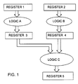
- this shows a typical digital electronic circuit with BIST facilities.
- the circuit consists of a number of blocks of logic (logic A-C) interconnected by a number of self-test registers (register 1-5).
- logic A-C logic A-C
- register 1-5 self-test registers
- test registers for BIST are described, for example in European Patent No 0196171 (US Patent No 4701916). [C1005]
- each of these self-test registers is set into its user mode, so that they all act as conventional latches.
- register 1 is set into the random mode so as to generate a pseudo-random sequence of test patterns at the inputs of logic block A.
- register 3 is set into the signature mode, so as to collect a series of outputs from logic block A, and to form a digital signature.
- the registers are all switched to the shift mode, to allow the test results to be serially shifted out over a serial path, and the generated signature is then compared with an expected signature value. If these values are not equal, a fault is indicated.
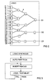
- the logic block consists of a number of logic cells (such as AND gates, NAND gates, OR gates, and so on), represented schematically as rectangles in the drawing, connected together in a network, between a number of inputs (I1-I26) and a number of outputs (O1-O3).
- logic cells such as AND gates, NAND gates, OR gates, and so on
- output O1 is influenced by inputs I1-I20
- output O2 is influenced by inputs I15-I22
- output O3 is influenced by inputs I23-I26.
- One way of overcoming this problem is to partition the logic block, by inserting additional self-test registers, referred to herein as fences , in such a manner that each fence bit splits off two or more input bits of a tree, i.e. isolates those input bits from the output of the tree.
- fences additional self-test registers
- the logic block could be partitioned by inserting a fence at the position indicated by *, so as to divide the tree into two independently testable sub-trees. It can be seen that the fence replaces the five inputs I1-I5 in the large tree with a single input, and so reduces the number of inputs that influence output O1 to 16.
- the object of the present invention is to provide a way of alleviating this problem.
- EP-A-0444806 describes a technique for testing an electronic circuit in which a logic cone is partitioned into sub-cones, having no more than w inputs each, by designating certain nodes in the cone as test points. This enables each sub-cone to be exhaustively tested. However, it does not consider the above-mentioned problem of placement of fences within a logic circuit.
- a design automation method for digital electronic circuits comprises the steps of synthesizing a circuit design including at least one logic tree having a plurality of inputs, and then automatically partitioning said logic tree by means of an automatic partitioning method comprising the steps:
- Figure 1 is a schematic block diagram of a digital electronic circuit.
- Figure 2 is a schematic block diagram of a logic block forming part of the circuit.
- Figure 3 is a flow chart showing the main components of a design automation process embodying the present invention.
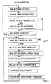
- Figure 4 is a flowchart showing an auto-partition program.
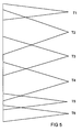
- Figure 5 is a schematic diagram showing the way in which logic trees are selected by the auto-partition program.
- Figure 6 is a flowchart showing a part of the auto-partition program, for finding possible fence points.
- Figure 7 is a schematic diagram of a logic tree, illustrating the way in which the auto-partition program finds possible fence points.
- this shows a design automation method for designing a digital electronic circuit.
- the circuit is first synthesized, using a logic synthesis program. This generates a number of logic blocks.
- the logic synthesis program may be a conventional, known design automation program, and so will not be described in any further detail.
- Each logic block is then processed by an auto-partitioning program, which partitions each block, as necessary, so that the maximum tree size in each block is equal to or less than the limit for exhaustive testing.
- the auto-partitioning program identifies the positions in which fences are to be inserted into the circuit to achieve this partitioning. The auto-partitioning program is described in more detail below.
- the fences specified by the auto-partitioning program are inserted into the design. This may be done automatically, or manually.
- the logic design is then checked, to ensure that it is testable. If this check is successful, then the design process is complete. If, on the other hand, the check is not successful, the positions of the fences are adjusted, and the check is repeated.
- Figure 4 shows the auto-partitioning program in more detail, showing the actions performed in processing a selected logic block.
- the program selects each output of the logic block in turn, and traces the tree back from this output, so as to find the inputs to that tree i.e. the inputs that influence this output.
- the number of inputs to the tree is compared with a predetermined value MAXINPUTS, equal to the maximum number of inputs that can be exhaustively tested. Typically, MAXINPUTS may be equal to 17. If the number of inputs to a tree is greater than MAXINPUTS, the tree is labelled as a "big" tree, and added to a list of big trees maintained by the auto-partitioning program.
- the list of big trees is examined. If the list is empty, there are no trees with more than the maximum permitted number of inputs, and so no partitioning is needed. If, on the other hand, there is at least one big tree on the list, the program proceeds as follows.
- one big tree is selected, and any other trees that overlap this tree are identified and added to a current set of trees. If any of these other trees are also big trees, any trees overlapping them are also identified and added to the current set. This process is repeated recursively until no more big trees can be found that overlap any big trees in the current set.
- This logic block comprises trees T1-T5, of which T2-T4 are big trees, and T1,T5 and T6 are small trees.
- tree T4 is initially selected and added to the current set.
- the program then adds trees T3 and T5 to the set, since they overlap big tree T4.
- tree T2 is added to the set, since it overlaps big tree T3.
- tree T1 is added to the set, since it overlaps big tree T2.
- tree T6 is not added to the set, since it overlaps only a small tree (T5) in the set.
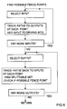
- the program then processes the current set of trees, so as to identify possible fence points, i.e. points at which fences may be positioned. Only points within the big trees of the set are considered as possible fence points.
- a point is identified as a possible fence point if it reduces the number of inputs to that tree, i.e. allows two or more bits of input to that tree to be replaced by a single fence bit at that point. If a point lies within the overlapping parts of the trees, all the trees at that point must be treated as a single entity; such a point is identified as a possible fence point only if it reduces the number of inputs to least one of the overlapping trees and does not increase the number of inputs to any of those trees. If this is not done, it is possible that a fence might be inserted which, while reducing the number of inputs to one tree, increases the number of inputs to another, overlapping tree. The way in which possible fence points are identified is described in more detail below.
- An optimization process is then performed, to optimize the positioning of the fence points. This process reduces the number of fence points, where possible, by replacing two or more fence points at a lower level of the tree by a fence point at a higher level. This is possible if the fence at the higher level would isolate all the input bits isolated by the fences at the lower level, and if the tree below the higher fence point contains fewer than the permitted maximum number of inputs MAXINPUTS.
- Figure 6 shows the way in which the auto-partition program identifies possible fence points within a tree (or set of overlapping trees).
- the program selects each input of the tree in turn, and traces each path through the tree from that input, adding the identity of the input to a driving bits list at each point of the tree. This constructs a driving bits list at each point, containing a list of all the tree inputs that affect that point.
- Figure 7 shows a typical logic tree consisting of logic cells L1-L12, and having inputs I1-I11.
- the driving bits list at each point 71-83 is indicated by numbers in square brackets.
- the driving bits list at point 79 is [4-8], indicating that this point is affected by inputs I4 to I8.
- the program selects each output of the tree in turn, and traces paths from that output back through the tree to the inputs.
- the program finds which input bits can be split at this point, and adds them to a splittable bits list for that point, containing a list of the tree input bits that can be isolated by insertion of a fence at this point.
- the splittable bits list for each point is indicated by numbers in round brackets. For example, the splittable bits list for point 81 is (1-2), indicating that input bits I1 and I2 can be isolated by a fence at this point.
- the program uses two alternative methods to determine the splittable bits: branch point analysis and slice analysis.
- splittable bits for each input branch to a logic cell are determined by finding the bits that are common to the splittable bits list of the output branch and the driving bits list for this input branch, and which do not also appear in the driving bits list of any other input branch to the same logic cell.
- splittable bits for input branch (splittable bits for output branch ⁇ driving bits for input branch) - driving bits for all other input branches where ⁇ represents set intersection (i.e. the bits common to the sets, and - represents set difference.
- bit 3 is not in the splittable bits set at this point, because it also appears at the other input branch 78 to the logic cell L12.
- Branch point analysis fails when it encounters reconvergent logic, i.e. logic with branches that divide at one logic cell and then merge together again at a subsequent logic cell, such as occurs between logic cells L7 and L12 in Figure 7. It can be seen that, in this case, branch point analysis would produce an empty splittable bits list at point 72, since the splittable bits lists at the outputs of logic cell L7 are both empty. However, it is clear that input bit I3 is splittable at this point. When branch point analysis fails, slice analysis is used.
- a logical level number is assigned to each point in the tree, starting from the output of the tree. Connections between cells are “stretched” as necessary so as to accommodate levels in parallel branches. For example, in Figure 7, the connection between logic cells L7 and L12 is “stretched” to accommodate the cell L10 in the parallel branch, so that the point 78 effectively exists at both level 1 and level 2.
- the splittable bits for any point at any level are determined by taking the driving bits for that point and subtracting the driving bits for all other points in a cross-section of the tree at the same logical level.
- Branch point analysis is more efficient than slice analysis, since it only needs to look at the input and output branches of one logic cell, whereas slice analysis needs to examine a cross section of the complete tree. Therefore, when determining the splittable bits list at any point, the program initially uses branch point analysis. If this produces an empty splittable bits list for the point, slice analysis is used.
- the program decides whether this point is a possible fence point.
- a point is considered suitable as a fence point only if the number of splittable bits at that point is greater than one.
- points 71, 73, 74, 75, 76, 79, 80, 81 and 82 are all possible fence points. If a point lies within the overlapping parts of two or more trees, a separate splittable bits list for that point is determined for each tree in which the point lies, and the point is considered suitable as a fence point only if at least one of these splittable bits lists contains more than one bit and the rest of these splittable bits lists each contain at least one bit. The point can then be used to split at least one tree, without a detrimental effect on the other trees.
Landscapes
- Engineering & Computer Science (AREA)
- General Engineering & Computer Science (AREA)
- Physics & Mathematics (AREA)
- General Physics & Mathematics (AREA)
- Tests Of Electronic Circuits (AREA)
- Design And Manufacture Of Integrated Circuits (AREA)
Abstract
Description
splittable bits for input branch
= (splittable bits for output branch
^ driving bits for input branch)
- driving bits for all other input branches
where ^ represents set intersection (i.e. the bits common to the sets, and - represents set difference.
splittable bits at
= (splittable bits at output of L12)
^ [driving bits at point 81]
- [driving bits at
= (1...11)^[1,2,3]-[3,4...11]
= [1,2,3]-[3,4...11]
= [1,2]
splittable bits at a point
= driving bits for the point
- driving bits for all other points at same logical level.
splittable bits at
= [driving bits at point 72]
- [driving bits at
= [3]-[1,2,4...11]
= [3].
Claims (6)
- A design automation method for digital electronic circuits, comprising the steps of synthesizing a circuit design including at least one logic tree having a plurality of inputs (I1-I11), and then automatically partitioning said logic tree by means of an automatic partitioning method comprising the steps:(a) identifying a set of driving bits for each of a set of points (71-83) within the tree, the set of driving bits for a point comprising all the tree inputs that affect that point;(b) identifying a set of splittable bits for each of said points, the set of splittable bits for a point comprising the tree inputs that would be isolated by insertion of a fence register at that point;(c) identifying which of said points are possible fence points, having more than one splittable bit; and(d) selecting a sub-set of said possible fence points, sufficient to reduce the number of inputs to the logic tree to a value less than a predetermined limit, and inserting fence registers at those points.
- A method according to Claim 1 wherein the step of identifying the set of splittable bits at a point comprises:(a) using a first method involving a local analysis of the driving bits and splittable bits in the vicinity of that point to derive the set of splittable bits for that point; and(b) if the first method fails, using a second method involving an analysis of the driving bits in a cross-section of the whole tree.
- A method according to Claim 1 or 2 wherein the step of identifying the splittable bits comprises tracing a path back from the output of said logic tree and, for each logic cell in said path, identifying the set of splittable bits for each input branch to the logic cell as the bits that are common to the set of splittable bits at the output branch of the logic cell and the set of driving bits for this input branch, and which do not also appear in the set of driving bits of any other input branch to the same logic cell.
- A method according to any preceding claim including a further step of optimizing the set of fence points, by replacing two or more fences in one level of the tree by a single fence at a higher level of the tree.
- A computer system, arranged to perform a design automation method in accordance with any one of claims 1 to 4.
- A digital electronic circuit, designed by a method in accordance with any one of Claims 1 to 4.
Applications Claiming Priority (2)
| Application Number | Priority Date | Filing Date | Title |
|---|---|---|---|
| GB9404078 | 1994-03-03 | ||
| GB9404078A GB9404078D0 (en) | 1994-03-03 | 1994-03-03 | Design automation method for digital electronic circuits |
Publications (2)
| Publication Number | Publication Date |
|---|---|
| EP0670552A1 EP0670552A1 (en) | 1995-09-06 |
| EP0670552B1 true EP0670552B1 (en) | 1998-06-24 |
Family
ID=10751213
Family Applications (1)
| Application Number | Title | Priority Date | Filing Date |
|---|---|---|---|
| EP94309357A Expired - Lifetime EP0670552B1 (en) | 1994-03-03 | 1994-12-14 | Design automation method for digital electronic circuits |
Country Status (4)
| Country | Link |
|---|---|
| US (1) | US5463562A (en) |
| EP (1) | EP0670552B1 (en) |
| DE (1) | DE69411259T2 (en) |
| GB (1) | GB9404078D0 (en) |
Families Citing this family (11)
| Publication number | Priority date | Publication date | Assignee | Title |
|---|---|---|---|---|
| JP2877023B2 (en) * | 1995-01-17 | 1999-03-31 | 日本電気株式会社 | Logic circuit division method |
| US5754824A (en) * | 1995-05-10 | 1998-05-19 | International Business Machines Corporation | Logic synthesis for logic array modules |
| US5661733A (en) * | 1996-04-10 | 1997-08-26 | Hughes Electronics | Automatic test insertion |
| US6551844B1 (en) | 1997-01-15 | 2003-04-22 | Formfactor, Inc. | Test assembly including a test die for testing a semiconductor product die |
| US6429029B1 (en) | 1997-01-15 | 2002-08-06 | Formfactor, Inc. | Concurrent design and subsequent partitioning of product and test die |
| US6557157B1 (en) | 1997-04-10 | 2003-04-29 | Boethel Andreas Frank | Method for designing complex digital and integrated circuits as well as a circuit structure |
| US6006027A (en) * | 1997-08-20 | 1999-12-21 | Synopsys, Inc. | Method and apparatus for event simulation |
| KR100522070B1 (en) * | 1998-12-31 | 2005-10-18 | 폼팩터, 인크. | Test method and assembly including a test die for testing a semiconductor product die |
| US6215325B1 (en) | 1999-03-29 | 2001-04-10 | Synopsys, Inc. | Implementing a priority function using ripple chain logic |
| US6493864B1 (en) * | 2001-06-20 | 2002-12-10 | Ammocore Technology, Inc. | Integrated circuit block model representation hierarchical handling of timing exceptions |
| US9092314B2 (en) * | 2012-12-19 | 2015-07-28 | Xilinx, Inc. | On-the-fly technical support |
Family Cites Families (9)
| Publication number | Priority date | Publication date | Assignee | Title |
|---|---|---|---|---|
| US4577276A (en) * | 1983-09-12 | 1986-03-18 | At&T Bell Laboratories | Placement of components on circuit substrates |
| US4908772A (en) * | 1987-03-30 | 1990-03-13 | Bell Telephone Laboratories | Integrated circuits with component placement by rectilinear partitioning |
| US4918614A (en) * | 1987-06-02 | 1990-04-17 | Lsi Logic Corporation | Hierarchical floorplanner |
| US4815003A (en) * | 1987-06-19 | 1989-03-21 | General Electric Company | Structured design method for high density standard cell and macrocell layout of VLSI chips |
| US4922432A (en) * | 1988-01-13 | 1990-05-01 | International Chip Corporation | Knowledge based method and apparatus for designing integrated circuits using functional specifications |
| US5187712A (en) * | 1990-02-26 | 1993-02-16 | At&T Bell Laboratories | Pseudo-exhaustive self-test technique |
| US5187671A (en) * | 1990-08-24 | 1993-02-16 | Microelectronics And Computer Technology Corporation | Automated interconnect routing system |
| US5202840A (en) * | 1990-12-19 | 1993-04-13 | Vlsi Technology, Inc. | Method for partitioning of connected circuit components before placement in one or more integrated circuits |
| US5189628A (en) * | 1991-03-11 | 1993-02-23 | National Semiconductor Corporation | System and method for partitioning PLA product terms into distinct logical groups |
-
1994
- 1994-03-03 GB GB9404078A patent/GB9404078D0/en active Pending
- 1994-12-14 EP EP94309357A patent/EP0670552B1/en not_active Expired - Lifetime
- 1994-12-14 DE DE69411259T patent/DE69411259T2/en not_active Expired - Fee Related
- 1994-12-20 US US08/359,519 patent/US5463562A/en not_active Expired - Fee Related
Also Published As
| Publication number | Publication date |
|---|---|
| EP0670552A1 (en) | 1995-09-06 |
| GB9404078D0 (en) | 1994-04-20 |
| DE69411259T2 (en) | 1999-01-28 |
| DE69411259D1 (en) | 1998-07-30 |
| US5463562A (en) | 1995-10-31 |
Similar Documents
| Publication | Publication Date | Title |
|---|---|---|
| Kajihara et al. | Cost-effective generation of minimal test sets for stuck-at faults in combinational logic circuits | |
| US5450414A (en) | Partial-scan built-in self-testing circuit having improved testability | |
| Tafertshofer et al. | A SAT-based implication engine for efficient ATPG, equivalence checking, and optimization of netlists | |
| Chen et al. | Structural and behavioral synthesis for testability techniques | |
| US5570376A (en) | Method and apparatus for identifying faults within a system | |
| US5455938A (en) | Network based machine instruction generator for design verification | |
| EP0670552B1 (en) | Design automation method for digital electronic circuits | |
| US4692921A (en) | Method for generating verification tests | |
| EP0444806A2 (en) | Pseudo-exhaustive self-test technique | |
| Chen et al. | Efficient BIST TPG design and test set compaction via input reduction | |
| US7266746B2 (en) | Device and method for testing integrated circuit | |
| US6408424B1 (en) | Verification of sequential circuits with same state encoding | |
| US6256770B1 (en) | Register transfer level (RTL) based scan insertion for integrated circuit design processes | |
| US6615392B1 (en) | Hierarchical design and test method and system, program product embodying the method and integrated circuit produced thereby | |
| Wu et al. | An efficient diagnosis-aware ATPG procedure to enhance diagnosis resolution and test compaction | |
| US5802075A (en) | Distributed test pattern generation | |
| US5566187A (en) | Method for identifying untestable faults in logic circuits | |
| US5548715A (en) | Analysis of untestable faults using discrete node sets | |
| KR20070007092A (en) | Test wrapper architecture, wrapper input / output cells and test methods thereof, integrated circuits, automated test devices | |
| US6185721B1 (en) | Method of design for testability at RTL and integrated circuit designed by the same | |
| US5559811A (en) | Method for identifying untestable and redundant faults in sequential logic circuits. | |
| Chen et al. | Behavioral synthesis for testability | |
| Zhao et al. | BETSY: synthesizing circuits for a specified BIST environment | |
| US7024606B2 (en) | Method of generating test pattern for integrated circuit | |
| Rudnick et al. | Probe point insertion for at-speed test |
Legal Events
| Date | Code | Title | Description |
|---|---|---|---|
| PUAI | Public reference made under article 153(3) epc to a published international application that has entered the european phase |
Free format text: ORIGINAL CODE: 0009012 |
|
| AK | Designated contracting states |
Kind code of ref document: A1 Designated state(s): DE FR GB IT NL |
|
| 17P | Request for examination filed |
Effective date: 19960112 |
|
| 17Q | First examination report despatched |
Effective date: 19970506 |
|
| GRAG | Despatch of communication of intention to grant |
Free format text: ORIGINAL CODE: EPIDOS AGRA |
|
| GRAG | Despatch of communication of intention to grant |
Free format text: ORIGINAL CODE: EPIDOS AGRA |
|
| GRAH | Despatch of communication of intention to grant a patent |
Free format text: ORIGINAL CODE: EPIDOS IGRA |
|
| GRAH | Despatch of communication of intention to grant a patent |
Free format text: ORIGINAL CODE: EPIDOS IGRA |
|
| ITF | It: translation for a ep patent filed | ||
| GRAA | (expected) grant |
Free format text: ORIGINAL CODE: 0009210 |
|
| AK | Designated contracting states |
Kind code of ref document: B1 Designated state(s): DE FR GB IT NL |
|
| REF | Corresponds to: |
Ref document number: 69411259 Country of ref document: DE Date of ref document: 19980730 |
|
| ET | Fr: translation filed | ||
| PLBE | No opposition filed within time limit |
Free format text: ORIGINAL CODE: 0009261 |
|
| STAA | Information on the status of an ep patent application or granted ep patent |
Free format text: STATUS: NO OPPOSITION FILED WITHIN TIME LIMIT |
|
| 26N | No opposition filed | ||
| PGFP | Annual fee paid to national office [announced via postgrant information from national office to epo] |
Ref country code: NL Payment date: 20011120 Year of fee payment: 8 |
|
| REG | Reference to a national code |
Ref country code: GB Ref legal event code: IF02 |
|
| PG25 | Lapsed in a contracting state [announced via postgrant information from national office to epo] |
Ref country code: NL Free format text: LAPSE BECAUSE OF NON-PAYMENT OF DUE FEES Effective date: 20030701 |
|
| NLV4 | Nl: lapsed or anulled due to non-payment of the annual fee |
Effective date: 20030701 |
|
| PGFP | Annual fee paid to national office [announced via postgrant information from national office to epo] |
Ref country code: FR Payment date: 20031110 Year of fee payment: 10 |
|
| PGFP | Annual fee paid to national office [announced via postgrant information from national office to epo] |
Ref country code: DE Payment date: 20031125 Year of fee payment: 10 |
|
| PG25 | Lapsed in a contracting state [announced via postgrant information from national office to epo] |
Ref country code: DE Free format text: LAPSE BECAUSE OF NON-PAYMENT OF DUE FEES Effective date: 20050701 |
|
| PG25 | Lapsed in a contracting state [announced via postgrant information from national office to epo] |
Ref country code: FR Free format text: LAPSE BECAUSE OF NON-PAYMENT OF DUE FEES Effective date: 20050831 |
|
| REG | Reference to a national code |
Ref country code: FR Ref legal event code: ST |
|
| PG25 | Lapsed in a contracting state [announced via postgrant information from national office to epo] |
Ref country code: IT Free format text: LAPSE BECAUSE OF NON-PAYMENT OF DUE FEES Effective date: 20051214 |
|
| PGFP | Annual fee paid to national office [announced via postgrant information from national office to epo] |
Ref country code: GB Payment date: 20091218 Year of fee payment: 16 |
|
| GBPC | Gb: european patent ceased through non-payment of renewal fee |
Effective date: 20101214 |
|
| PG25 | Lapsed in a contracting state [announced via postgrant information from national office to epo] |
Ref country code: GB Free format text: LAPSE BECAUSE OF NON-PAYMENT OF DUE FEES Effective date: 20101214 |