EP0667687A1 - Echo canceller - Google Patents
Echo canceller Download PDFInfo
- Publication number
- EP0667687A1 EP0667687A1 EP95101789A EP95101789A EP0667687A1 EP 0667687 A1 EP0667687 A1 EP 0667687A1 EP 95101789 A EP95101789 A EP 95101789A EP 95101789 A EP95101789 A EP 95101789A EP 0667687 A1 EP0667687 A1 EP 0667687A1
- Authority
- EP
- European Patent Office
- Prior art keywords
- digital signals
- signals
- receiver
- coefficients
- terminals
- Prior art date
- Legal status (The legal status is an assumption and is not a legal conclusion. Google has not performed a legal analysis and makes no representation as to the accuracy of the status listed.)
- Granted
Links
- 238000002592 echocardiography Methods 0.000 claims description 8
- 230000000694 effects Effects 0.000 claims description 6
- 238000000034 method Methods 0.000 claims description 6
- 238000010276 construction Methods 0.000 claims description 2
- 238000004519 manufacturing process Methods 0.000 claims 4
- 230000001934 delay Effects 0.000 abstract description 4
- RYGMFSIKBFXOCR-UHFFFAOYSA-N Copper Chemical compound [Cu] RYGMFSIKBFXOCR-UHFFFAOYSA-N 0.000 description 40
- 229910052802 copper Inorganic materials 0.000 description 40
- 239000010949 copper Substances 0.000 description 40
- 238000010586 diagram Methods 0.000 description 12
- 230000005540 biological transmission Effects 0.000 description 9
- 239000013307 optical fiber Substances 0.000 description 7
- 230000008901 benefit Effects 0.000 description 5
- 230000000750 progressive effect Effects 0.000 description 4
- 230000001360 synchronised effect Effects 0.000 description 4
- 230000004913 activation Effects 0.000 description 3
- 238000005516 engineering process Methods 0.000 description 3
- 230000015556 catabolic process Effects 0.000 description 2
- 238000012937 correction Methods 0.000 description 2
- 125000004122 cyclic group Chemical group 0.000 description 2
- 238000006731 degradation reaction Methods 0.000 description 2
- 230000001419 dependent effect Effects 0.000 description 2
- 230000008030 elimination Effects 0.000 description 2
- 238000003379 elimination reaction Methods 0.000 description 2
- 230000009467 reduction Effects 0.000 description 2
- 230000003213 activating effect Effects 0.000 description 1
- 230000006978 adaptation Effects 0.000 description 1
- 238000004364 calculation method Methods 0.000 description 1
- 230000008859 change Effects 0.000 description 1
- 238000004891 communication Methods 0.000 description 1
- 239000002131 composite material Substances 0.000 description 1
- 230000001143 conditioned effect Effects 0.000 description 1
- 230000008878 coupling Effects 0.000 description 1
- 238000010168 coupling process Methods 0.000 description 1
- 238000005859 coupling reaction Methods 0.000 description 1
- 238000001514 detection method Methods 0.000 description 1
- 239000000284 extract Substances 0.000 description 1
- 239000000203 mixture Substances 0.000 description 1
- 230000004044 response Effects 0.000 description 1
- 238000005070 sampling Methods 0.000 description 1
- 230000009897 systematic effect Effects 0.000 description 1
- 230000007704 transition Effects 0.000 description 1
Images


Classifications
-
- H—ELECTRICITY
- H04—ELECTRIC COMMUNICATION TECHNIQUE
- H04B—TRANSMISSION
- H04B3/00—Line transmission systems
- H04B3/02—Details
- H04B3/20—Reducing echo effects or singing; Opening or closing transmitting path; Conditioning for transmission in one direction or the other
- H04B3/23—Reducing echo effects or singing; Opening or closing transmitting path; Conditioning for transmission in one direction or the other using a replica of transmitted signal in the time domain, e.g. echo cancellers
- H04B3/237—Reducing echo effects or singing; Opening or closing transmitting path; Conditioning for transmission in one direction or the other using a replica of transmitted signal in the time domain, e.g. echo cancellers using two adaptive filters, e.g. for near end and for end echo cancelling
Definitions
- This invention relates to systems for, and methods of, passing digital data at high frequencies through copper telephone lines between a central station and subscribers serviced by the central station and recovering the data at the receiving end of the telephone lines.
- This invention further relates to systems for, and methods of, providing for such transmission and reception without any repeaters in the telephone lines.
- Telephone systems are organized on a systematic basis.
- a central station is provided to service all of the subscribers within a particular radius such as approximately one (1) mile from the central station.
- a subscriber serviced by the central station wishes to make a telephone call, he dials a sequence of numbers identifying the party called. Signals representing this sequence of numbers then pass through the telephone lines from the caller to the central station. The sequence of dialed numbers are then transmitted from the central station through other telephone lines to the central station of the party being called. This central station then channels the call to the telephone of the party being called.
- optical fibers have largely replaced copper telephone lines between the central station servicing the telephone of the calling party and the central station of the party being called. This is particularly true when the call being made is a long distance call.
- Optical fibers are advantageous because they can transmit signals at data rates with minimal losses in power and minimal degradation in system fidelity.
- Optical fibers are also advantageous because they can handle a large number of different calls simultaneously without any interference between the calls.
- Copper wires are still generally used between the central stations and the subscribers serviced by such central stations. Copper wires have inherent disadvantages. They provide relatively large power losses, particularly in relation to optical fibers. This causes the fidelity of the signals to be degraded as the signals pass through the copper telephone lines. Copper lines also provide interference between different calls travelling through adjacent copper wires. Because of these negative factors involved in the use of copper wires in telephone systems, it would be desirable to replace the copper wires with optical fibers as quickly as possible. However, this is a daunting task, particularly in view of the large number of subscribers. At the present time, it is contemplated that optical fibers will not completely replace the copper wires until well into the twenty first (21 st) century.
- repeaters Because of the power losses and the degradation in signal fidelity in the copper wires, repeaters have had to be disposed at spaced intervals between the central station and the subscriber. The repeaters act to boost the signals after they have deteriorated while passing through the telephone lines. As many as two (2) or three (3) repeaters have often had to be provided between the central station and the subscriber.
- Repeaters are disadvantageous. They consume power and require space. Furthermore, in order to operate properly, they often are disposed below the ground (as in manholes) at displaced positions between the central station and the subscriber. The position of a repeater previously disposed below the ground for boosting the signals between the central station and a particular subscriber is often difficult to locate, particularly since the copper lines between the central station and the particular subscriber first have to be located and these lines are often disposed below ground.
- analog signals representing individual digital values (+/-1, +/-3) pass through a telephone line to a receiver. These signals may be first provided in a pseudo random sequence.
- a linear echo canceller and a first adder eliminate, to an extent, echo signals resulting from second analog signals transmitted on the same telephone line by the receiver.
- a non-linear echo canceller and a second adder further eliminate the echo signals and specifically reduce non-linear components in the echo signals. Adjustable signal delays achieve optimal performance of the linear and non-linear echo cancellers.
- an equalizer containing four (4) different modules then compensates for signal distortions introduced by the telephone line and minimizes the effect of noise present in the telephone line.
- the equalizer modules are a digital gain control element, a feed forward digital filter, and two (2) feedback digital filters.
- a detector module in application (attorneys file D-2755) produces in one of several different ways at the receiver an estimate of the digital data (+/-1, +/-3) transmitted at the other end of the telephone line.
- the detector either extracts the digital information based on peaks in the received (non- equalized) signal, or by adding the equalized signal with preset threshold values.
- a scrambler-descrambler module in application locally generates a replica of the digital symbols transmitted in analog form at the other end of the telephone line, based on a limited number (e.g. 23) of correctly detected digital values.
- the scrambler-descrambler module may also operate as a descrambler to recover data scrambled by the transmitter at the other end.
- analog signals representing individual digital values ( + 3, + 1,-1,-3) of data pass through a telephone line to a receiver. These signals may be first provided in a pseudo random sequence.
- a linear echo canceller and a first adder at the receiver simultaneously eliminate, to a considerable extent, echo signals resulting from second analog signals transmitted through the telephone line by the receiver.
- a non-linear echo canceller and a second adder further significantly reduce the echo signals and specifically reduce non-linear components in the echo signals.
- each echo canceller includes a member which stores signals representing for each terminal in such echo canceller (a) the pseudo random sequence and (b) coefficients for adjusting the signals in such sequence.
- Such data for each terminal in such echo canceller is recorded in the memory for introduction to the next terminal in the memory.
- the signals representing the data from the associated adder and the output from the associated adder are processed to determine an adjusted value of such coefficient for storage in the memory and for use in the next cycle of processing.
- This adjusted coefficient value and the data stored in the memory for such terminal are processed to produce signals for introduction to the associated adder.
- the signals from the second adder are processed to restore the data transmitted through the telephone lines to the receiver.
- the echo canceller of this invention also has other advantages over the prior art. It operates with only a single port, which receives the address for individual signals in the echo canceller. This is in contrast to the prior art echo cancellers, which have required two (2) ports. Furthermore, the data in the memory of the echo canceller of this invention is sampled before the signals representing such data have settled, and the sampled signals are used to write data into the memory. This has increased the data rate at which the echo canceller of this invention can operate.
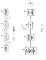
- FIG. 1 illustrates a system now in use for transmitting aural (e.g. voice) signals and data signals between a central station 10 and a subscriber's location 12.
- the central station 10 is able to communicate with all of the subscribers, including the subscriber 12, within a particular radius such as approximately one (1) mile from the central station.
- the communication generally occurs through copper lines 14. These copper lines have often been in place for many years. They have effectively transmitted voice signals between the central station 10 and the subscriber 12 but with power losses and some signal distortion.
- the system shown in Figure 1 has been relatively effective because voice signals occur at relatively low frequencies - generally to a maximum of about three thousand hertz (3 Khz). Furthermore, if there has been an occasional distortion in the signals transmitted through the copper lines, this occasional distortion has not affected the ability of the person at the receiving end to hear and understand the audio message. In other words, the subscriber is often willing to overlook minor and instantaneous distortions in the audio information that he or she receives as long as the audio information is understandable and does not appear aurally to be distorted.
- receivers 16 have been provided in the copper lines 14 at spaced intervals between the central station 10 and the subscriber 12.
- the repeaters 16 may be considered as amplifiers which restore power to the data signals and restore the high frequency components to such signals.
- one (1) to three (3) repeaters 16 are disposed in the copper lines 14 between the central station 10 and the subscriber 12.
- This invention provides a different system than that of Pairgain for accomplishing substantially the same results.
- the system of this invention is at least the equal of the system provided by Pairgain Technologies.
- the error rate in the transmission of data signals through the copper lines 14 in this system is no greater than, and may be slightly less than, the error rate in the transmission of such data signals by the system of Pairgain Technologies.
- repeaters 16 do not have to be provided in the copper lines 14 between the central station 10 and the subscriber location 12 when the system of this invention is provided at the central station 10 and the subscriber location 12.
- a transmitter generally indicated at 20 in Figure 2 and a receiver generally indicated at 22 in Figure 3 are disposed in a composite housing at each of the central station 10 and the subscriber location 12.
- the transmitter 20 and the receiver 22 are disposed in a common housing.
- the transmitter 20 and the receiver 22 are shown in separate Figures for purposes of clarity.
- the transmitter 20 includes a stage 23 which provides data signals having four (4) analog levels representing digital data values of + 3, + ,-1 and -3.
- Each of the four (4) analog levels represents a pair of digital signals having a coded pattern individual to such analog level. This may be seen from the following table.
- the digital data produced in the stage 23 to represent an individual sequence of analog values is combined as at 24 with digital signals in a pseudo random pattern of binary 1's and 0's.
- This pseudo random pattern is individual to the particular transmitter.
- the transmitter 20 at the central station 10 may provide a different pseudo random code than the transmitter at the subscriber location 12.
- the resultant digital signals may be filtered as at 26 to pass signals only in a particular range of frequencies within the transmission capabilities of the copper lines 14.
- the filtered signals are converted by a digital-to- analog converter 28 to corresponding analog signals and the analog signals are transmitted through the copper lines 14.
- the transmitter 20 described above and shown in Figure 2 is well known in the art. However, it is novel, at least in co-pending application (attorneys file D-2755) when combined in a system with the receiver 22 shown in Figure 3.
- the receiver 22 shown in Figure 3 may be considered to be included in one embodiment of the invention.
- the receiver 22 receives the data signals (combined with the pseudo random code) passing through the copper lines 14 from the transmitter 20. These signals are converted by an analog-to-digital converter 30 to corresponding digital signals.
- the digital signals are introduced to an adder or summing device 32 which compares the digital signals from the converter 30 with digital signals from a linear echo canceller 34.
- the linear echo canceller 34 in turn receives signals in a pseudo random code from a stage 36.
- the adder or summing device 32 and the linear echo canceller 34 are included in stages generally indicated at 35 for eliminating echoes from the signals received by the receiver 22. The stages 35 are enclosed within a box in broken lines.
- the transmitter 20 in Figure 2 is at the central station 10 and that the receiver 22 in Figure 3 is at the subscriber location 12.
- the pseudo random code at the central station 10 is individual to the central station and the pseudo random code at the subscriber location 12 is individual to the subscriber location.
- the pseudo random code at the subscriber location is combined with the digital signals representing digital data transmitted from the subscriber location 12 to the central station 10. These combined digital signals are reflected with some intensity by the transmitter 20 at the central station 10 and the reflected or echo signals are received at the receiver 22 at the subscriber location 12.
- the digital signals received at the receiver 22 are a mixture of the digital signals (combined with a first code) transmitted from the transmitter 20 at the central station 12 and digital signals (combined in a second pseudo random code) transmitted from the subscriber location.
- the digital signals combined with the second pseudo random code are transmitted in analog form from the subscriber location 12 to the central station 10 and are reflected by the central station back to the subscriber location.
- the linear echo canceller 34 co-operates with the adder 32 to eliminate on a coarse basis the echo or reflected signals combined with the second pseudo random code.
- the adder 32 removes the reflected or echo signals by simultaneously adding or subtracting a sequence of approximately one hundred and twenty eight (128) digital signals from the converter 30 and the linear echo canceller 34.
- the resultant signals at the output of the adder 32 are introduced back to the linear echo canceller 34 to change the coefficients at one hundred and twenty eight (128) progressive taps in the linear echo canceller.
- the linear echo canceller 34 has an optimal effect in removing any echoes or reflections from the digital signals provided by the converter.
- the continuous adjustments in the coefficients of the linear echo canceller 34 are indicated by a line (partially broken) at the top and bottom of the rectangle indicating the linear echo canceller). Such line extends from the output of the adder 32 diagonally through the box designated as the linear echo canceller 34 and terminates with a downwardly pointing arrow at a position just below such box. Similar arrangements are shown in other stages where continuous adjustments in coefficients are being made.
- the signals from the adder 32 are introduced to another adder or summing device 40 which also receives digital signals from a non-linear echo canceller 42.
- the inclusion of the non-linear echo canceller 42 constitutes one of the key features of this invention, particularly in the embodiment shown in the drawings and described subsequently.
- the adder or summing device 40 and the non-linear echo canceller 42 are included in the stages indicated in broken lines at 35 in Figure 3.
- the non-linear echo canceller 42 receives the signals from the modulator 36 in the same pseudo random code as the linear echo canceller 34. However, the non-linear echo canceller 42 has only a minimal number of (e.g. 3) of taps in comparison to the one hundred and twenty (120) taps in the linear echo canceller 34.
- the signals at the taps in the non-linear echo canceller 42 are simultaneously introduced to the adder or summing device 40 to eliminate further any of the signals echoed or reflected from the transmitter 20.
- the output from the adder or summing device 40 is introduced to the taps in the non-linear echo canceller 42 to adjust the coefficients at the taps in such canceller. This provides for an optimal operation of the non-linear echo canceller 42 in removing at each instant the echoes or reflections received at the receiver 22 from the transmitter 20.
- the non-linear echo canceller 42 illustratively operates with only three (3) adjustable coefficients as against illustratively one hundred and twenty (120) adjustable coefficients for the linear echo canceller 34, the non-linear echo canceller provides a further significant reduction in the echo signals passing through the telephone lines 14 from the transmitter 20 to the receiver 22. It complements the operation of the linear echo canceller by significantly reducing echo signal components that are non-linear in nature and thus are not capable of being eliminated by the echo canceller 34.
- the echo canceller 42 may be constructed in a manner similar to that of the echo canceller 34. However, the use of a non-linear echo canceller such as the canceller 42 is not believed to be known in the prior art for providing a fine further significant reduction of the echo signals in the lines 14.
- the digital signals from the adder or summing device 40 pass to a gain control stage 46 in an equalizer which is shown in broken lines and which is generally indicated at 48 in Figure 3.
- the gain control stage 46 adjusts the gain of the digital signals from the adder or summing device 40 to a particular level.
- the gain control stage 46 has a plurality of taps each with an individual coefficient. These coefficients are continuously adjusted by the output signals from an adder or summing device 50.
- the operation of the adder or summing device 50 will be described in detail subsequently.
- a gain control stage with adjustable coefficients corresponding to the gain control stage 46 may be known in the prior art.
- the output from the gain control stage 46 is introduced to a feed forward equalizer 50 in the equalizer 48.
- the feed forward equalizer 50 may be known in the prior art. It operates on the digital signals from the gain control stage 46 to eliminate the effects on each such pairs of delays from previous pairs of the digital signals in the signals received by the receiver 22. This is accomplished by providing feedbacks from the adder 50 to the feed forward equalizer 52 to adjust the coefficients at the individual ones of the plurality of taps in this equalizer.
- the adjusted signals from the feed forward equalizer 52 pass to an adder or summing device 54 in the equalizer 48 as do the pairs of signals in a decision feedback equalizer 56 which is also in the equalizer 48.
- the decision feedback analyzer 56 may be known in the prior art.
- the decision feedback analyzer 56 receives from a multiplexer 58 the digital signals representing the data received by the receiver 22.
- the digital signals from the multiplexer 58 adjust a plurality of coefficients in the decision feedback equalizer 56 in accordance with the characteristics of these signals.
- the decision feedback analyzer 56 eliminates any tails on the digital signals passing through the copper lines 14 to the receiver 22 to represent data. These tails result from the differences in the responses of the copper lines to different frequencies in the digital signals representing the data.
- An adder or summing device 60 receives the signals from the adder or summing device 54.
- the adder or summing device 60 and the multiplexer 58 are included in a detector generally indicated in broken lines at 61.
- the adder 60 receives digital signals from an error predictor 62 which may be known in the art and which is included in the detector 61.
- the error predictor 62 includes a noise predictor which operates in a well known manner upon the signals from the multiplexer 58 to eliminate noise. In eliminating such noise, the error predictor 60 converts the noise signals in an unpredictable pattern to error signals which have a predictable pattern.
- the error predictor 62 includes stages which eliminate the errors in the predictable pattern in such signals.
- the error predictor 62 has a plurality of taps with adjustable coefficients.
- the error predictor 62 adjusts the coefficients at these taps in accordance with the characteristics of the signals from an adder or summing device 63. These signals are produced in accordance with a comparison of the signals from the adder or summing device 60 and the multiplexer 58.
- the digital signals from the transmitter 20 have a simplified pseudo random code to simplify the ability of the receiver 22 to become synchronized quickly with the operation of the transmitter 20.
- a synchronization as quickly as possible between the operations of the transmitter 20 and the receiver 22 is desirable so that the receiver 22 will be able to receive data thereafter from the transmitter 20. This is particularly desirable when the synchronization occurs after an interruption in the coupling through the copper lines 14 between the transmitter 20 and the receiver 22 because data cannot be transmitted between the transmitter and the receiver until such synchronization occurs.
- only a few seconds of difference in the synchronization between the transmitter 20 and the receiver 22 is important since the ability to transmit important data is lost during the period of non- synchronization.
- the simplified pseudo random code in the transmitter 20 is provided by a pattern of signals at analog values of only +3 and -3. By providing analog values of only +3 and -3, the time for synchronizing the operations of the transmitter 20 and the receiver 22 should be minimized.
- the pairs of the digital signals in the simplified pseudo random code are transmitted for a period as long as seven (3) seconds but the synchronization generally occurs well before the end of this period.
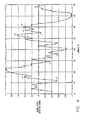
- the digital signals in the simplified pseudo random code are introduced from the adder 40 to a peak detector 66 which may be known in the prior art.
- the peak detector 66 is included in the detector 61.
- the peak detector 66 operates upon the signals from the adder or summing device 40 to detect positive and negative peaks in the patterns of these pairs of signals. Positive peaks indicate an analog value of + and negative peaks indicate an analog value of -3.
- the operation of the peak detector 66 may illustratively be seen from Figure 4 which illustrates digital signals introduced from the adder 40 to the peak detector 66. As shown in Figure 4, some of the positive peaks are illustratively designated in Figure 4 as "+3". Similarly, some of the negative peaks are illustratively designated in Figure 4 as "-3".
- the signals detected by the peak detector 66 to indicate analog values of + 3 and -3 are introduced to a multiplexer 70 in Figure 1.
- the multiplexer 70 is included in the detector 61.
- the multiplexer 70 also receives digital signals from a slicer 72 which is included in the detector 61.
- a slicer such as the slicer 72 may be known in the prior art.
- the slicer 72 determines whether the digital value of each pair of digital signals from the adder or summing device 60 is closer to an analog value of +3 or to an analog value of -3.
- the slicer provides the pair of digital signals with a value of +3.
- the slicer 72 provides the pair of digital signals with a value of -3 when the digital signals in the pair indicate an analog value closer to -3 than to +3.
- the multiplexer 70 receives the digital signals from the peak detector 66 and from the slicer 72.
- the multiplexer 70 ordinarily provides a higher priority to the peak detector 66 than to the slicer 72.
- the multiplexer 70 passes the signals from the peak detector 66 when it simultaneously receives signals from the peak detector and the slicer. It will be appreciated that the multiplexer 70 may provide priority to the signals from the slicer 72 rather than to the signals from the peak detector 66.
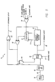
- the signals passing through the multiplexer 70 are introduced to a scrambler-descrambler generally indicated at 74 in Figure 1.
- the scrambler-descrambler 74 is included in the detector 61.
- the scrambler-descrambler constitutes one of the key features of the invention disclosed and claimed in co-pending application (attorneys file D-2755).
- the scrambler-descrambler 74 receives a particular number (e.g. 23) of the successive pairs of the digital signals from the multiplexer 70 and generates a sequence of successive digital signals from such particular number of the digital signals from the multiplexer.
- the sequence of such signals is dependent upon an algorithm corresponding to the algorithm for the simplified pseudo random code transmitted from the transmitter 20 during the initial period of synchronism of the transmitter and the receiver.
- the sequence of such signals from the scrambler-descrambler 74 is compared in the adder 50 with the sequence of the signals from the multiplexer 70. This comparison continues until a particular percentage (e.g. 90%) of the signals from the scrambler-descrambler 74 and from the multiplexer 70 coincide. When this occurs, the system is considered to be in synchronization and the comparison of the signals from the scrambler-descrambler 74 and the multiplexer 70 is discontinued.
- the signals from the multiplexer 70 are then introduced through the multiplexer 58 to the adder or summing device 50 for comparison with the signals from the adder or summing device 54.
- the signals from the multiplexer 70 are also introduced through the multiplexer 58 to the gain control stage 46 and the feed forward equalizer 52 to adjust the operation of these stages.
- the stage 74 also constitutes a descrambler. After the initial period when the stage 74 operates as a scrambler as described above to synchronize the operation of the transmitter and the receiver 22, the stage 74 operates as a descrambler of the signals from the multiplexer 70. In operating as a descrambler, the stage 74 removes the pseudo random code in the pairs of the digital signals representing the data from the transmitter 20 so that the digital signals passing to output lines 78 represent only the data. The signals on the output lines 78 are introduced to a channel unit interface 80 and from the interface 80 to a decoder 82 for recovering the data in the digital signals passing through the telephone lines 14.
- the scrambler-descrambler 74 includes lines 80 which receive the output from the multiplexer 70 (also shown in Figure 3).
- the signals on the lines 80 are introduced to a stage 82 which converts parallel inputs for each pair of signals representing an analog value (+3, + 1,-1,-3) to serial inputs of such signals.
- the output from the stage 82 is introduced to an input terminal of a multiplexer 84 having another input terminal connected to the output of an exclusive OR network 86.
- the multiplexer 84 also receives a control signal on a line 87 when the multiplexer is to operate in the descramble mode.
- the output from the multiplexer 84 is introduced to a line 88 when the system shown in Figure 5 is operating in the scrambler mode. In this mode, the signals on the line 88 constitute the output of the scrambler.
- the output from the multiplexer 84 also passes to scrambler-descrambler registers 90 when the system shown in Figure 5 is operating either as a scrambler or a descrambler.
- the scrambler-descrambler register 90 operates as specialized shift registers, different embodiments of which are shown in Figures 6-9 and described in detail subsequently.
- the scrambler-descrambler registers 90 include a plurality (e.g. 23) of flip-flops connected in a sequence.
- the output from the last flip-flop (e.g. flip-flop 23) is introduced to an exclusive OR network 92.
- the exclusive OR network 92 also receives the output from a multiplexer 94.
- the multiplexer 94 has two (2) inputs, one from the output of the fifth (5th) flip-flop in the scrambler-descrambler registers 90 and the other from the output of the eighteenth (18th) flip-flop in the scrambler-descrambler registers.
- one of the outputs from the scrambler-descrambler registers 90 is effective with the operation of the registers at the central station 10 and the other output is effective with the operation of the registers at the remote location.
- the multiplexer 94 also receives on a control line the output from an exclusive OR network 96.
- An input is provided to the exclusive OR network 96 from a line 98 which controls the operation in a descramble mode of the system shown in Figure 5.
- Another input to the exclusive OR network 96 receives the signals through a line 99 from a particular one of the shift register networks shown in Figures 8 and 9 depending upon whether the system shown in Figure 5 is at the central station 10 or at the subscriber location 12.
- the output of the exclusive OR network 92 is common with one input terminal of an exclusive OR network 100.
- a second input terminal of the exclusive OR network 100 and a second input terminal of the exclusive OR network 86 receive the output signals from the stage 82.
- the output from the exclusive OR network 100 is introduced to the line 78 (also shown in Figure 1) when the system shown in Figure 5 is operating as a descrambler.
- Figures 6 and 7 respectively indicate how the pseudo random code is generated at the transmitter 20.
- the system shown in Figure 6 generates the pseudo random code at the transmitter 20 when the transmitter is at the subscriber location 12 and the receiver 22 is at the central station 10.
- the system shown in Figure 7 generates the pseudo random code at the transmitter 20 when the transmitter is at the central station 10 and the receiver 22 is at the subscriber location 12.
- the system shown in Figure 6 includes a plurality of flip-flops which may be respectively designated as 102a, 102b...102n.
- the output of each flip-flop in the sequence is connected to the input of the next flip-flop in the sequence.
- the flip-flop 102n is illustratively the twenty third (23rd) flip-flop in the sequence.
- the output of this flip-flop is introduced to an adder or summing device 104 as is the output illustratively from the eighteenth (18th) flip-flop in the sequence.
- the resultant output from the adder or summing device 104 is introduced to an adder or summing device 106 as is the input on a line 108.
- the output from the adder or summing device 106 in turn passes to an input line 110 which is connected to the input of the first flip-flop in the sequence.
- the system shown in Figure 6 generates a pseudo random code at the central station when the transmitter 20 is at the subscriber location 12 and the receiver 22 is at the central station 10.
- the system shown in Figure 7 is the same as the system shown in Figure 6 except that the output of the fifth (5th) flip-flop in the sequence is illustratively connected to an adder or summing device 112 corresponding to the adder 104 in Figure 6.
- the system shown in Figure 7 generates a pseudo random code when the transmitter 20 is at the central station 10 and the receiver 22 is at the subscriber location.
- the arrangement shown in Figure 6 produces in a pseudo random code signals which are introduced to the modulating stage 23 in the transmitter 22 of Figure 3 when the transmitter is at the subscriber location 12. These signals modulate the data signals from the stage 23 in Figure 2. The resultant signals are filtered in Figure 2 and converted to analog form. The stages shown in Figure 3 and described above recover these signals in the pseudo random code and introduce these signals to the multiplexer 70 common to Figures 3 and 5. The multiplexer 70 then passes these signals to the scrambler-descrambler registers 90.
- Figures 8 and 9 illustrate the construction of the scrambler-descrambler registers 90 in Figure 5 when the registers are at the receiver 22.
- the embodiment shown in Figure 8 is operative in the receiver 22 in the central station 10 when the embodiment shown in Figure 6 is transmitting signals in the pseudo random code from the subscriber location 12.
- the embodiment shown in Figure 8 introduces the output from the eighteenth (18th) flip-flop to an adder or summing device 116 just as the output from the eighteenth (18th) flip-flop in Figure 6 is introduced to the adder or summing device 104 in Figure 6.
- the input is introduced through a line 117 to a flip-flop 118a constituting the first of the successive flip-flops in the shift register.
- the input on the line 117 and the output from the adder 116 are also introduced to an adder 120.
- the output from the adder or summing device 120 passes to a line 121. This is opposite to the input and output in the system shown in Figure 6.
- the system shown in Figure 9 is used in the receiver 22 at the subscriber location 12 when the transmitter 20 sends signals from the central station 10 to the subscriber location 12.
- the system shown in Figure 9 introduces the output of the fifth (5th) flip-flop to an adder or summing device 122. This corresponds to the introduction of the output of the fifth (5th) flip-flop to the adder or summing device 112 in Figure 7.
- the output from the adder or summing device 122 passes to an adder or summing device 124 as does the input on a line 126.
- the input on the line 126 also passes to a flip-flop 128 which constitutes the first flip-flop in a sequence.
- the output from the adder 124 passes to a line 130.
- either the output from the fifth (5th) flip-flop or the eighteenth (18th) flip-flop in the register 90 passes through the multiplexer 94 depending upon whether the scrambler-descrambler is in the receiver 22 at the central station 10 or at the subscriber location 12.
- the signals from the multiplexer 94 in turn pass to the exclusive OR network 92 as do the signals from the output (the 23rd flip-flop) of the registers 90.
- the signals from the multiplexer 94 and from the twenty third (23rd) flip-flop in the register 90 are compared in the exclusive OR network 92 such that, when one (1) (but not both) of the input signals to the multiplexer is a binary "1", a signal passes through the exclusive OR network 92 to the exclusive "OR" network 86.
- the exclusive OR network 86 in turn operates on the signals from the exclusive OR network 92 and the signals from the stage 86 to pass signals to the multiplexer 84.
- the multiplexer 84 provides a priority in the signals from the exclusive OR network 86 over the signals from the stage 82 when the scrambler-descrambler is operating in the scrambler mode.
- the signals passing through the multiplexer 84 are introduced to the registers 90 after the registers 90 have received the first twenty three (23) signals from the stage 82. In this way, the registers 90 generate a code, after the first twenty three (23) signals passing through the multiplexer 70, dependent upon the characteristics from the exclusive OR network 86.
- the signals from the multiplexer 86 also pass to the line 88 when the scrambler-descrambler is operating as a scrambler.
- the signals on the line 88 pass to the multiplexer 58 ( Figure 3) which also receives the signals from the multiplexer 70.
- the user has an option of determining whether to grant a priority to the passage through the multiplexer 58 of the signals on the line 88 or the signals from the multiplexer 70.
- the signals from the multiplexer 58 are introduced to the adder or summing device 50 for comparison with the signals from the adder or summing device 54.
- the resultant signals from the adder or summing device 50 adjust the coefficients at the taps in the stages 46 and 52.
- signals representing data are transmitted from the transmitter to the receiver.
- the digital signals passing through the line 80 for the successive analog values are converted by the stage 82 from a parallel representation to a series representation.
- the signals then pass through the multiplexer 84, which is conditioned by the signals on the line 87 to provide a priority to the signals from the stage 82 over the signals from the exclusive OR network 86.
- the passage of signals through the multiplexer 94 occurs as a result of the passage through the line 98 and the exclusive OR network 92 of a signal indicating the operation in the descramble mode of the system shown in Figure 5.
- the signals passing through the multiplexer 94 are combined with the signals from the last (the 23rd) flip-flop from the registers 90.
- the resultant signals then pass to the exclusive OR network 100 which also receives the signals from the stage 82.
- the output from the exclusive OR network 100 then passes to the output line 78 as the digital indications of the data from the transmitter 20.
- the output from the exclusive OR network 100 also passes to the adder or summing device 50 in Figure 3 for comparison with the output from the adder or summing device 54 as described above.
- the system and method described above have certain important advantages. They assure that the echo signals at the receiver 22 are efficiently removed. This is particularly significant when it is considered that the echo signals at the receiver may often have a strength at least five hundred percent (500%) greater than the signals passing through the lines 14 to represent data.
- This efficient cancellation of the echo signals is provided on a first basis as by the linear echo canceller 34 and the adder or summing device in Figure 3 and on a further basis as by the non-linear echo canceller 44 and the adder or summing device 40 in Figure 3.
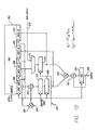
- Figure 10 is a circuit diagram, partially in block form, illustrating one embodiment of the invention.
- the embodiment shown in Figure 10 includes a storage memory 200 having a pair of input terminals 202 and 204.
- the input terminal 202 receives input data and the input terminal 204 receives input information relating to coefficients at a particular terminal in the echo canceller.
- the storage memory 200 also has a port 205 for introducing to the memory signals representing the coefficients and data at individual ones of the different taps or terminals in the linear echo canceller 34.
- the echo canceller of this invention is advantageous because it uses only the single port 205 to address the memory 204.
- the prior art uses more than one (1) port.
- the storage memory 200 additionally has a pair of output terminals 206 and 208.
- the terminal 206 receives data output from the storage memory 200 and the terminal 208 receives from the storage member 200 output information relating to coefficients.
- the terminals 202 and 206 provide information relating to coefficients for adjusting the signals introduced to the linear echo canceller 34 and the non-linear echo canceller 42 from the pseudo random code modulator 36.
- the pseudo random modulator 36 provides the code for combination with the data transmitted from the receiver to the transmitter and reflected from the transmitter back to the receiver.
- the signals on a line 210 from the pseudo random code modulator 36 pass to a multiplexer 212 which also receives signals from the terminal 206 in the storage memory 200.
- the signals passing through the multiplexer 212 are introduced to a register 214 which synchronizes the passage of signals through the register with clock signals on a line 216.
- the signals from the register 214 are introduced to the terminal 202 in the storage memory 200 as the data input to the storage member.
- the signals from the register 214 also pass to a multiplier 218.
- the multiplier 218 also receives the output from a register 220.
- the register 220 also introduces its output to the terminal 204 for storage in the storage memory 200 as information relating to coefficients.
- the operation of the register 220 is synchronized with the clock signal on the line 216 as is the operation of a register 222.
- the output of the register 222 is common with the input of the register 220 and the input of the register 222 is common with the output of an adder 224.
- the adder 224 receives inputs from the terminal 208 in the storage memory 200 and from a multiplier 226.
- the multiplier 226 has one (1) input terminal connected to the terminal 206 in the storage memory 200 and has another input terminal connected to a line 230.
- the output from the multiplier 218 is introduced to an adder or summing device 232.
- the adder 232 also receives the signals from a register 234, the operation of which is synchronized with the clock signal on the line 216.
- the output from the register 234 is introduced as an input to the adder 232.
- the output from the register 234 also passes through a line 236 as an input to an individual one of the linear echo canceller 34 or the non-linear echo canceller 42.
- the linear echo canceller 34 has a plurality (e.g. 120) of terminals or taps. Each of these terminals receives signals from the pseudo random code modulator 36. Upon each generation of a pair of digital signals in the modulator 36 to represent an individual analog level (+ 3, + 1,-1,-3), the pairs of signals previously generated by the modulator shift progressively to a successive terminal in the linear echo canceller 34.
- Each of the terminals in the linear echo canceller has at any instant an adjustable coefficient which modifies the pseudo random signal at that instant.
- This adjustable coefficient shifts to the next terminal in the echo canceller 34 when the next pseudo random signal is generated in the modulator 36. At the same time, the coefficient is adjusted in accordance with the output from the adder 32.
- the non-linear echo canceller 42 operates in a manner similar to the linear echo canceller 34.
- the non-linear echo canceller 42 has a significantly lower number (e.g.3) of terminals than the linear echo canceller 34. This causes the corrections provided by the non-linear echo canceller 42 to be more precise than the corrections provided by the linear echo canceller 34.
- the linear echo canceller 34 can be considered to provide a coarse elimination at the receiver 22 of the signals transmitted by the receiver to the transmitter 10 and reflected by the transmitter back to the receiver.
- the non-linear echo canceller 42 can be considered to provide a fine elimination of such echo signals.
- the resultant system provides a significantly more precise detection of the data transmitted from the transmitter 20 to the receiver 22 than the systems of the prior art.
- Figure 10 provides an illustration of the data introduced to one (1) terminal of the linear echo canceller 34 at an instant in time. It will be appreciated that a plurality of systems to that shown in Figure 10 are provided for the other terminals in the linear echo canceller 34, one (1) such system being provided for each individual one (1) of the terminals in such echo canceller. It will also be seen that a plurality of systems similar to that shown in Figure 10 are provided for the individual terminals in the linear echo canceller 42, one (1) such system being provided for each individual one (1) of the terminals in such echo canceller.
- the line 236 is designated as providing signals from the linear echo canceller 34 or the non-linear echo canceller 42 and has used this line on a generic basis for all of the different terminals in each of the echo cancellers 34 and 42.
- signals are introduced to the multiplexer 212 from the output terminal 206 of the storage member 200. These signals represent a byte in the pseudo random code from the modulator 36 in Figure 1. These signals pass to the register 214 which operates at the time of the next clock signal on the line 216 to pass the signals to the terminal 202 for recording in the storage memory 200. Four cycles later, these signals pass through the output terminal 206, the multiplexer 212 and the register 214 to the input terminal 202 of the storage member 200. The reason for the delay of four (4) cycles will be seen from the subsequent discussion.
- the signals representing the pseudo random code are shifted from each terminal in the linear echo canceller 34 to the next terminal in the echo canceller upon each progressive occurrence of a clock signal on the line 216.
- this shift cannot occur because the shift of four (4) clock cycles is greater than the number of terminals left in the echo canceller. Because of this, a signal passes from the pseudo random code echo canceller 34 through the line 210, the multiplexer 212 to the register 214 when the signals from the modulator 36 have been shifted to the last three (3) terminals of the echo canceller 34.
- the terminal 208 in the storage memory 200 passes the coefficient from the storage member 200 for a particular terminal in the echo canceller 208. These signals are introduced to the adder or summing device 204 as are the signals from the multiplier 226.
- the multiplier receives the signals on the line 230. These signals are provided at the output of the adder 32 for the particular terminal. They represent the error produced to the adder 32 for that particular terminal, this error being designated by the symbol y. These signals are multiplied by a constant represented by the symbol ⁇ .
- the multiplier 226 multiplies the error value l1.y and the data B introduced to the particular terminal from the output terminal 206 of the storage member.
- the data B represents one of the bytes in the pseudo random code from the modulator 36.
- the resultant value l1.yB is added in the adder 224 with the coefficient previously provided at such particular terminal. These signals are shifted in time by progressive constants of time in accordance with the clock signals introduced to the registers 222 and 220.
- the resultant signals at the output of the register 220 represent the new value of the coefficient for the particular terminal in the echo canceller 34. This new value for the coefficient at the particular terminals of the echo canceller 34 is recorded at the terminal 204 in the storage member 200.
- the value represented by the data signals from the register 214 and the new value of the coefficient from the register 220 are multiplied in the stage 218.
- the resultant signals are introduced to the register 234 which synchronizes the signals with the clock signals on the line 216.
- the output signals from the register 234 are in turn added with the signals from the multiplier 218.
- the adder 232 and the register 234 operate as an integrator to produce the signals cumulatively representing the signals which are introduced from the particular terminal in the echo canceller 34 to the adder 32 for comparison with the signals from the analog-to-digital converter 30.
- Figure 11 constitutes a chart which illustrates how coefficients are shifted through the storage memory 200.
- the first column in Figure 11 indicates the successive cycles of the clock signals on the line 216.
- the second column indicates the times at which successive coefficients are recorded in the memory member 200 through the terminal 204 in Figure 10.
- Column 3 in Figure 10 indicates the times at which the successive coefficients previously recorded in the memory member 200 are read from the memory member at the terminal 208.
- the middle three (3) columns in Figure 11 respectively correspond to the first three (3) columns of Figure 11.
- the middle three (3) columns of Figure 11 indicate the timing sequence for the next symbol after the symbol of the first three (3) columns. This may be seen from the designation of "Symbol O" at the bottom of the first three (3) columns and the designation of "Symbol 1 " at the bottom of the middle three (3) columns.
- the first three (3) columns indicate the coefficient at a first terminal in the linear echo canceller 34 and the middle three (3) columns indicate the coefficient at the next terminal in the linear echo canceller.
- the last three (3) columns of Figure 11 indicate the coefficient at a third (3rd) terminal directly after the first two (2) terminals in the linear echo canceller 32.
- the input B from the pseudo random code modulator 36 advances from one terminal to the next in the echo canceller in successive clock signals.
- the filter coefficient E for a particular terminal in the echo canceller is adjusted in each clock cycle and the adjusted coefficient is introduced to the same terminal in the next clock cycle.
- the value E ; , k is produced at the output terminal of the register 220 and is introduced to the terminal 204 in the memory member 200 as the new value of the coefficient for the terminal i in the echo canceller.
- the value e K represents the digital signals produced at the particular terminal (the k terminal) in the echo canceller.
- Figure 12 indicates, primarily in block form, circuitry for reading data from the memory 204, processing the data and providing for the introduction of the processed data to the memory. Circuitry corresponding to that shown in Figure 12 is provided for reading coefficients from the memory 204, processing the coefficients and introducing the processed coefficients to the memory. The only difference would be that the words "DATA” and "DATA” would be respectively replaced by the words --COEFFICIENT-- and --COEFFICIENT-- in such circuitry.
- "DATA” and "DATA” signals are respectively introduced from the memory 204 to sample-and-hold stages 250 and 252.
- the signals in the stages 250 and 252 are sampled at particular instants of time on a cyclic basis in accordance with timing signals introduced on a line 254 to these stages.
- the timing signals are provided on the line 254 before the signals in the sample-and-hold stages 250 and 252 have settled to their final values.
- the differential signals from the sample-and-hold stages 250 and 252 pass to a sense amplifier 254.
- the signals from the sense amplifier 254 are latched as at 256.
- the signals from the latch 256 are introduced to the stage 224 in Figure 10.
- the signals from the register 214 in Figure 10 are introduced to an amplifier 260 and an amplifier-inverter 262 in Figure 12.
- the amplifier 260 and the amplifier-inverter 262 in Figure 12 are activated by the cyclic signal on the line 254. However, the activation of the amplifier 260 and the amplifier-inverter 262 occurs at a different time in each cycle than the activation of the sample-and-hold circuits 250 and 252.
- the signals from the amplifier 260 and the amplifier-inverter 262 are stored in the memory 204. By activating the sample-and-hold circuits 250 and 252 at different times than the activation of the amplifier 260 and the amplifier-inverter 262, the reading of data from the memory 204 does not interfere with the writing of data into the memory and vice versa.
- the echo canceller represented by the circuit diagram shown in Figure 10 for an individual terminal in the echo canceller 34 or the echo canceller 42 and described above has certain important advantages. It uses a single storage memory 200 for storing all of the information which such echo canceller uses in processing information. Furthermore, the use of the storage memory 200 assures that the information introduced to the echo canceller will be processed properly.
- the echo canceller of Figure 10 is also more simple and straightforward than the echo cancellers of the prior art. It provides a performance at least equal to any echo canceller of the prior art.
Landscapes
- Engineering & Computer Science (AREA)
- Computer Networks & Wireless Communication (AREA)
- Signal Processing (AREA)
- Cable Transmission Systems, Equalization Of Radio And Reduction Of Echo (AREA)
- Telephonic Communication Services (AREA)
- Filters That Use Time-Delay Elements (AREA)
Abstract
Description
- This invention relates to systems for, and methods of, passing digital data at high frequencies through copper telephone lines between a central station and subscribers serviced by the central station and recovering the data at the receiving end of the telephone lines. This invention further relates to systems for, and methods of, providing for such transmission and reception without any repeaters in the telephone lines.
- Telephone systems are organized on a systematic basis. A central station is provided to service all of the subscribers within a particular radius such as approximately one (1) mile from the central station. When a subscriber serviced by the central station wishes to make a telephone call, he dials a sequence of numbers identifying the party called. Signals representing this sequence of numbers then pass through the telephone lines from the caller to the central station. The sequence of dialed numbers are then transmitted from the central station through other telephone lines to the central station of the party being called. This central station then channels the call to the telephone of the party being called.
- Telephone systems have been partially upgraded in recent years. For example, optical fibers have largely replaced copper telephone lines between the central station servicing the telephone of the calling party and the central station of the party being called. This is particularly true when the call being made is a long distance call. Optical fibers are advantageous because they can transmit signals at data rates with minimal losses in power and minimal degradation in system fidelity. Optical fibers are also advantageous because they can handle a large number of different calls simultaneously without any interference between the calls.
- Even though optical fibers are generally now used between different central stations, copper wires are still generally used between the central stations and the subscribers serviced by such central stations. Copper wires have inherent disadvantages. They provide relatively large power losses, particularly in relation to optical fibers. This causes the fidelity of the signals to be degraded as the signals pass through the copper telephone lines. Copper lines also provide interference between different calls travelling through adjacent copper wires. Because of these negative factors involved in the use of copper wires in telephone systems, it would be desirable to replace the copper wires with optical fibers as quickly as possible. However, this is a monumental task, particularly in view of the large number of subscribers. At the present time, it is contemplated that optical fibers will not completely replace the copper wires until well into the twenty first (21 st) century.
- Because of the power losses and the degradation in signal fidelity in the copper wires, repeaters have had to be disposed at spaced intervals between the central station and the subscriber. The repeaters act to boost the signals after they have deteriorated while passing through the telephone lines. As many as two (2) or three (3) repeaters have often had to be provided between the central station and the subscriber.
- Repeaters are disadvantageous. They consume power and require space. Furthermore, in order to operate properly, they often are disposed below the ground (as in manholes) at displaced positions between the central station and the subscriber. The position of a repeater previously disposed below the ground for boosting the signals between the central station and a particular subscriber is often difficult to locate, particularly since the copper lines between the central station and the particular subscriber first have to be located and these lines are often disposed below ground.
- The need for installing repeaters between the central station and the subscribers serviced by the central station has become magnified in recent years. This has resulted from the fact that data signals as well as voice signals have been transmitted through the copper lines in recent years. Data signals occur at higher data rates than voice signals. This has caused the power losses in the copper lines and the distortions in the fidelity of the signals transmitted through the copper lines to become magnified. Furthermore, data signals illustratively transmitted from a central station to a subscriber are reflected at the subscriber's location back to the central station. These signals interfere at the central station with the data signals transmitted from the subscriber's location to the central station and prevent the data signals from being decoded clearly. The clear decoding of data is important because errors in data are not as easily tolerated as errors in sound. For example, an error in the transmission of data representing numerical values can become considerably compounded as numerical computations involving such error progress.
- In one embodiment of an invention, disclosed and claimed in application Serial No. - (attorneys file D-2755) filed on , 1994, by Eric Paneth, Mordechai Segal, Boaz Rippin and Ehud H. Rokach, and assigned of record to the assignee of record of this application, analog signals representing individual digital values (+/-1, +/-3) pass through a telephone line to a receiver. These signals may be first provided in a pseudo random sequence. A linear echo canceller and a first adder eliminate, to an extent, echo signals resulting from second analog signals transmitted on the same telephone line by the receiver. A non-linear echo canceller and a second adder further eliminate the echo signals and specifically reduce non-linear components in the echo signals. Adjustable signal delays achieve optimal performance of the linear and non-linear echo cancellers.
- In co-pending application (attorneys file D-2755), an equalizer containing four (4) different modules then compensates for signal distortions introduced by the telephone line and minimizes the effect of noise present in the telephone line. The equalizer modules are a digital gain control element, a feed forward digital filter, and two (2) feedback digital filters.
- A detector module in application (attorneys file D-2755) produces in one of several different ways at the receiver an estimate of the digital data (+/-1, +/-3) transmitted at the other end of the telephone line. The detector either extracts the digital information based on peaks in the received (non- equalized) signal, or by adding the equalized signal with preset threshold values.
- A scrambler-descrambler module in application (attorneys file D-2755) locally generates a replica of the digital symbols transmitted in analog form at the other end of the telephone line, based on a limited number (e.g. 23) of correctly detected digital values. The scrambler-descrambler module may also operate as a descrambler to recover data scrambled by the transmitter at the other end.
- In one embodiment of this invention, analog signals representing individual digital values ( + 3, + 1,-1,-3) of data pass through a telephone line to a receiver. These signals may be first provided in a pseudo random sequence. A linear echo canceller and a first adder at the receiver simultaneously eliminate, to a considerable extent, echo signals resulting from second analog signals transmitted through the telephone line by the receiver. A non-linear echo canceller and a second adder further significantly reduce the echo signals and specifically reduce non-linear components in the echo signals.
- In one inventive embodiment, each echo canceller includes a member which stores signals representing for each terminal in such echo canceller (a) the pseudo random sequence and (b) coefficients for adjusting the signals in such sequence. Such data for each terminal in such echo canceller is recorded in the memory for introduction to the next terminal in the memory. For each terminal in such echo canceller, the signals representing the data from the associated adder and the output from the associated adder are processed to determine an adjusted value of such coefficient for storage in the memory and for use in the next cycle of processing. This adjusted coefficient value and the data stored in the memory for such terminal are processed to produce signals for introduction to the associated adder. The signals from the second adder are processed to restore the data transmitted through the telephone lines to the receiver.
- The echo canceller of this invention also has other advantages over the prior art. It operates with only a single port, which receives the address for individual signals in the echo canceller. This is in contrast to the prior art echo cancellers, which have required two (2) ports. Furthermore, the data in the memory of the echo canceller of this invention is sampled before the signals representing such data have settled, and the sampled signals are used to write data into the memory. This has increased the data rate at which the echo canceller of this invention can operate.
- In the drawings:
- Figure 1 is a simplified block diagram of a system of the prior art for transmitting signals representing digital data signals through copper lines between an individual one of a central station and a subscriber location and for receiving and decoding the digital data signals at the other one of the central station and the subscriber location;
- Figure 2 is a simplified block diagram of a transmitter disposed at the individual one of the central station and the subscriber location and included in one embodiment of the invention for transmitting signals representing digital data through copper lines to the other one of the central station and the subscriber location;
- Figure 3 is a simplified block diagram of a receiver disposed at the other one of the central station and the subscriber location and included in one embodiment of the invention;
- Figure 4 illustrates a sequence of signals produced at progressive instants of time at one of the stages shown in Figure 3;
- Figure 5 is a somewhat detailed circuit diagram in block form of another of the stages shown in Figure 3 when the stage is used as a scrambler or is used as a descrambler;
- Figure 6 is a circuit diagram in block form of a system included at the subscriber location for generating digital signals in a pseudo random code for transmission to the central station when the system shown in Figure 5 is being used at the central station;
- Figure 7 is a circuit diagram in block form of a system included at the central station for generating digital signals in a pseudo random code for transmission to the subscriber location when the system shown in Figure 5 is being used at the subscriber location;
- Figure 8 is a circuit diagram in block form of a system included at the central station for generating digital signals in a pseudo random code station when the system shown in Figure 5 is being used to transmit data signals from the subscriber location to the central station;
- Figure 9 is a circuit diagram in block form of a system included at the subscriber location for generating digital signals in a pseudo random code when the system shown in Figure 5 is being used to transmit data signals from the central station to the subscriber location;
- Figure 10 is a circuit diagram, partly in block form, of an echo canceller included in the system shown in Figure 1, such echo canceller constituting one embodiment of the invention;
- Figure 11 is a chart illustration of the operation of the echo canceller shown in Figure 10; and
- Figure 12 is a circuit diagram, primarily in block form, of circuitry associated with the echo canceller shown in Figure 10.
- Figure 1 illustrates a system now in use for transmitting aural (e.g. voice) signals and data signals between a
central station 10 and a subscriber'slocation 12. Thecentral station 10 is able to communicate with all of the subscribers, including thesubscriber 12, within a particular radius such as approximately one (1) mile from the central station. The communication generally occurs throughcopper lines 14. These copper lines have often been in place for many years. They have effectively transmitted voice signals between thecentral station 10 and thesubscriber 12 but with power losses and some signal distortion. - The system shown in Figure 1 has been relatively effective because voice signals occur at relatively low frequencies - generally to a maximum of about three thousand hertz (3 Khz). Furthermore, if there has been an occasional distortion in the signals transmitted through the copper lines, this occasional distortion has not affected the ability of the person at the receiving end to hear and understand the audio message. In other words, the subscriber is often willing to overlook minor and instantaneous distortions in the audio information that he or she receives as long as the audio information is understandable and does not appear aurally to be distorted.
- In recent years, data has been transmitted through the
copper lines 14 between the central station and the subscriber. This data has been transmitted through thecopper lines 14 at data rates significantly higher than the frequencies of the audio information transmitted through the telephone lines. Such data has had to be received by the subscriber with considerable accuracy. For example, if the data represents numerical information, an error in the reception of such numerical information may cause subsequent numerical information derived from the numerical information with the error to be inaccurate. Sometimes an error in the reception of numerical information may even become compounded by subsequent calculations involving such numerical information that the error becomes enormous. - Since the data transmitted through the
copper lines 14 is at relatively high frequencies, the power losses in thecopper lines 14 increase and the distortions produced in the transmission of the data through the telephone lines also increase. To compensate for these difficulties,receivers 16 have been provided in thecopper lines 14 at spaced intervals between thecentral station 10 and thesubscriber 12. Therepeaters 16 may be considered as amplifiers which restore power to the data signals and restore the high frequency components to such signals. Generally one (1) to three (3)repeaters 16 are disposed in thecopper lines 14 between thecentral station 10 and thesubscriber 12. - It has been recognized for some time that the disposition of the
repeaters 16 in thecopper lines 14 between thecentral station 10 and thesubscriber 12 is not the ultimate solution to the problems discussed above. Repeaters are expensive. They also consume power. Furthermore, they provide a fair, but far from perfect, restoration of the characteristics of the signals in thelines 14. They are also disposed below ground. Because of this, it is often difficult to locate thecopper lines 14 of theindividual subscriber 12 and to connect one or more of therepeaters 16 in these copper lines. - Recently a system has been provided by Pairgain Technologies for operating on the data signals passing through the
copper lines 14 so that the data information is transmitted with fidelity between thecentral station 10 and thesubscriber location 12. Because of this, repeaters 16 do not have to be provided in thecopper lines 14 between thecentral station 10 and thesubscriber location 12. This system has quickly achieved considerable recognition. Units of this system are being sold in large quantities to the regional telephone companies and to other customers. - This invention provides a different system than that of Pairgain for accomplishing substantially the same results. The system of this invention is at least the equal of the system provided by Pairgain Technologies. For example, the error rate in the transmission of data signals through the
copper lines 14 in this system is no greater than, and may be slightly less than, the error rate in the transmission of such data signals by the system of Pairgain Technologies. Furthermore,repeaters 16 do not have to be provided in thecopper lines 14 between thecentral station 10 and thesubscriber location 12 when the system of this invention is provided at thecentral station 10 and thesubscriber location 12. - In one embodiment of the invention, a transmitter generally indicated at 20 in Figure 2 and a receiver generally indicated at 22 in Figure 3 are disposed in a composite housing at each of the
central station 10 and thesubscriber location 12. Generally thetransmitter 20 and thereceiver 22 are disposed in a common housing. However, thetransmitter 20 and thereceiver 22 are shown in separate Figures for purposes of clarity. Thetransmitter 20 includes astage 23 which provides data signals having four (4) analog levels representing digital data values of + 3, + ,-1 and -3. Each of the four (4) analog levels represents a pair of digital signals having a coded pattern individual to such analog level. This may be seen from the following table.
- The digital data produced in the
stage 23 to represent an individual sequence of analog values is combined as at 24 with digital signals in a pseudo random pattern of binary 1's and 0's. This pseudo random pattern is individual to the particular transmitter. For example, thetransmitter 20 at thecentral station 10 may provide a different pseudo random code than the transmitter at thesubscriber location 12. The resultant digital signals may be filtered as at 26 to pass signals only in a particular range of frequencies within the transmission capabilities of the copper lines 14. The filtered signals are converted by a digital-to-analog converter 28 to corresponding analog signals and the analog signals are transmitted through the copper lines 14. Thetransmitter 20 described above and shown in Figure 2 is well known in the art. However, it is novel, at least in co-pending application (attorneys file D-2755) when combined in a system with thereceiver 22 shown in Figure 3. - The
receiver 22 shown in Figure 3 may be considered to be included in one embodiment of the invention. Thereceiver 22 receives the data signals (combined with the pseudo random code) passing through thecopper lines 14 from thetransmitter 20. These signals are converted by an analog-to-digital converter 30 to corresponding digital signals. The digital signals are introduced to an adder or summingdevice 32 which compares the digital signals from theconverter 30 with digital signals from alinear echo canceller 34. Thelinear echo canceller 34 in turn receives signals in a pseudo random code from astage 36. The adder or summingdevice 32 and thelinear echo canceller 34 are included in stages generally indicated at 35 for eliminating echoes from the signals received by thereceiver 22. Thestages 35 are enclosed within a box in broken lines. - Assume that the
transmitter 20 in Figure 2 is at thecentral station 10 and that thereceiver 22 in Figure 3 is at thesubscriber location 12. As previously described, the pseudo random code at thecentral station 10 is individual to the central station and the pseudo random code at thesubscriber location 12 is individual to the subscriber location. The pseudo random code at the subscriber location is combined with the digital signals representing digital data transmitted from thesubscriber location 12 to thecentral station 10. These combined digital signals are reflected with some intensity by thetransmitter 20 at thecentral station 10 and the reflected or echo signals are received at thereceiver 22 at thesubscriber location 12. Thus the digital signals received at thereceiver 22 are a mixture of the digital signals (combined with a first code) transmitted from thetransmitter 20 at thecentral station 12 and digital signals (combined in a second pseudo random code) transmitted from the subscriber location. The digital signals combined with the second pseudo random code are transmitted in analog form from thesubscriber location 12 to thecentral station 10 and are reflected by the central station back to the subscriber location. - The
linear echo canceller 34 co-operates with theadder 32 to eliminate on a coarse basis the echo or reflected signals combined with the second pseudo random code. Theadder 32 removes the reflected or echo signals by simultaneously adding or subtracting a sequence of approximately one hundred and twenty eight (128) digital signals from theconverter 30 and thelinear echo canceller 34. The resultant signals at the output of theadder 32 are introduced back to thelinear echo canceller 34 to change the coefficients at one hundred and twenty eight (128) progressive taps in the linear echo canceller. - By continuously adjusting the coefficients at the different taps in the
linear echo canceller 34 in accordance with the results of the comparison in the adder or summingdevice 32, thelinear echo canceller 34 has an optimal effect in removing any echoes or reflections from the digital signals provided by the converter. The continuous adjustments in the coefficients of thelinear echo canceller 34 are indicated by a line (partially broken) at the top and bottom of the rectangle indicating the linear echo canceller). Such line extends from the output of theadder 32 diagonally through the box designated as thelinear echo canceller 34 and terminates with a downwardly pointing arrow at a position just below such box. Similar arrangements are shown in other stages where continuous adjustments in coefficients are being made. - The signals from the
adder 32 are introduced to another adder or summingdevice 40 which also receives digital signals from a non-linear echo canceller 42. The inclusion of the non-linear echo canceller 42 constitutes one of the key features of this invention, particularly in the embodiment shown in the drawings and described subsequently. The adder or summingdevice 40 and the non-linear echo canceller 42 are included in the stages indicated in broken lines at 35 in Figure 3. The non-linear echo canceller 42 receives the signals from themodulator 36 in the same pseudo random code as thelinear echo canceller 34. However, the non-linear echo canceller 42 has only a minimal number of (e.g. 3) of taps in comparison to the one hundred and twenty (120) taps in thelinear echo canceller 34. - The signals at the taps in the non-linear echo canceller 42 are simultaneously introduced to the adder or summing
device 40 to eliminate further any of the signals echoed or reflected from thetransmitter 20. The output from the adder or summingdevice 40 is introduced to the taps in the non-linear echo canceller 42 to adjust the coefficients at the taps in such canceller. This provides for an optimal operation of the non-linear echo canceller 42 in removing at each instant the echoes or reflections received at thereceiver 22 from thetransmitter 20. - Since the non-linear echo canceller 42 illustratively operates with only three (3) adjustable coefficients as against illustratively one hundred and twenty (120) adjustable coefficients for the
linear echo canceller 34, the non-linear echo canceller provides a further significant reduction in the echo signals passing through thetelephone lines 14 from thetransmitter 20 to thereceiver 22. It complements the operation of the linear echo canceller by significantly reducing echo signal components that are non-linear in nature and thus are not capable of being eliminated by theecho canceller 34. - The echo canceller 42 may be constructed in a manner similar to that of the
echo canceller 34. However, the use of a non-linear echo canceller such as the canceller 42 is not believed to be known in the prior art for providing a fine further significant reduction of the echo signals in thelines 14. - The digital signals from the adder or summing
device 40 pass to again control stage 46 in an equalizer which is shown in broken lines and which is generally indicated at 48 in Figure 3. Thegain control stage 46 adjusts the gain of the digital signals from the adder or summingdevice 40 to a particular level. Thegain control stage 46 has a plurality of taps each with an individual coefficient. These coefficients are continuously adjusted by the output signals from an adder or summingdevice 50. The operation of the adder or summingdevice 50 will be described in detail subsequently. A gain control stage with adjustable coefficients corresponding to thegain control stage 46 may be known in the prior art. - The output from the
gain control stage 46 is introduced to a feedforward equalizer 50 in theequalizer 48. The feed forwardequalizer 50 may be known in the prior art. It operates on the digital signals from thegain control stage 46 to eliminate the effects on each such pairs of delays from previous pairs of the digital signals in the signals received by thereceiver 22. This is accomplished by providing feedbacks from theadder 50 to the feed forwardequalizer 52 to adjust the coefficients at the individual ones of the plurality of taps in this equalizer. - The adjusted signals from the feed forward
equalizer 52 pass to an adder or summingdevice 54 in theequalizer 48 as do the pairs of signals in adecision feedback equalizer 56 which is also in theequalizer 48. Thedecision feedback analyzer 56 may be known in the prior art. Thedecision feedback analyzer 56 receives from amultiplexer 58 the digital signals representing the data received by thereceiver 22. The digital signals from themultiplexer 58 adjust a plurality of coefficients in thedecision feedback equalizer 56 in accordance with the characteristics of these signals. Thedecision feedback analyzer 56 eliminates any tails on the digital signals passing through thecopper lines 14 to thereceiver 22 to represent data. These tails result from the differences in the responses of the copper lines to different frequencies in the digital signals representing the data. - An adder or summing
device 60 receives the signals from the adder or summingdevice 54. The adder or summingdevice 60 and themultiplexer 58 are included in a detector generally indicated in broken lines at 61. Theadder 60 receives digital signals from anerror predictor 62 which may be known in the art and which is included in thedetector 61. Theerror predictor 62 includes a noise predictor which operates in a well known manner upon the signals from themultiplexer 58 to eliminate noise. In eliminating such noise, theerror predictor 60 converts the noise signals in an unpredictable pattern to error signals which have a predictable pattern. Theerror predictor 62 includes stages which eliminate the errors in the predictable pattern in such signals. Theerror predictor 62 has a plurality of taps with adjustable coefficients. Theerror predictor 62 adjusts the coefficients at these taps in accordance with the characteristics of the signals from an adder or summingdevice 63. These signals are produced in accordance with a comparison of the signals from the adder or summingdevice 60 and themultiplexer 58. - In an initial period of a few seconds, the digital signals from the
transmitter 20 have a simplified pseudo random code to simplify the ability of thereceiver 22 to become synchronized quickly with the operation of thetransmitter 20. A synchronization as quickly as possible between the operations of thetransmitter 20 and thereceiver 22 is desirable so that thereceiver 22 will be able to receive data thereafter from thetransmitter 20. This is particularly desirable when the synchronization occurs after an interruption in the coupling through thecopper lines 14 between thetransmitter 20 and thereceiver 22 because data cannot be transmitted between the transmitter and the receiver until such synchronization occurs. As will be appreciated, only a few seconds of difference in the synchronization between thetransmitter 20 and thereceiver 22 is important since the ability to transmit important data is lost during the period of non- synchronization. - The simplified pseudo random code in the
transmitter 20 is provided by a pattern of signals at analog values of only +3 and -3. By providing analog values of only +3 and -3, the time for synchronizing the operations of thetransmitter 20 and thereceiver 22 should be minimized. The pairs of the digital signals in the simplified pseudo random code are transmitted for a period as long as seven (3) seconds but the synchronization generally occurs well before the end of this period. - The digital signals in the simplified pseudo random code are introduced from the
adder 40 to apeak detector 66 which may be known in the prior art. Thepeak detector 66 is included in thedetector 61. Thepeak detector 66 operates upon the signals from the adder or summingdevice 40 to detect positive and negative peaks in the patterns of these pairs of signals. Positive peaks indicate an analog value of + and negative peaks indicate an analog value of -3. The operation of thepeak detector 66 may illustratively be seen from Figure 4 which illustrates digital signals introduced from theadder 40 to thepeak detector 66. As shown in Figure 4, some of the positive peaks are illustratively designated in Figure 4 as "+3". Similarly, some of the negative peaks are illustratively designated in Figure 4 as "-3". The signals detected by thepeak detector 66 to indicate analog values of + 3 and -3 are introduced to amultiplexer 70 in Figure 1. Themultiplexer 70 is included in thedetector 61. - The
multiplexer 70 also receives digital signals from aslicer 72 which is included in thedetector 61. A slicer such as theslicer 72 may be known in the prior art. During the transmission of the pairs of signals with the simplified pseudo random code, theslicer 72 determines whether the digital value of each pair of digital signals from the adder or summingdevice 60 is closer to an analog value of +3 or to an analog value of -3. When the digital value of a pair of digital signals is closer to any analog value of + than to an analog value of -3, the slicer provides the pair of digital signals with a value of +3. Similarly, theslicer 72 provides the pair of digital signals with a value of -3 when the digital signals in the pair indicate an analog value closer to -3 than to +3. - As previously described, the
multiplexer 70 receives the digital signals from thepeak detector 66 and from theslicer 72. Themultiplexer 70 ordinarily provides a higher priority to thepeak detector 66 than to theslicer 72. In other words, themultiplexer 70 passes the signals from thepeak detector 66 when it simultaneously receives signals from the peak detector and the slicer. It will be appreciated that themultiplexer 70 may provide priority to the signals from theslicer 72 rather than to the signals from thepeak detector 66. The signals passing through themultiplexer 70 are introduced to a scrambler-descrambler generally indicated at 74 in Figure 1. The scrambler-descrambler 74 is included in thedetector 61. The scrambler-descrambler constitutes one of the key features of the invention disclosed and claimed in co-pending application (attorneys file D-2755). - The scrambler-
descrambler 74 receives a particular number (e.g. 23) of the successive pairs of the digital signals from themultiplexer 70 and generates a sequence of successive digital signals from such particular number of the digital signals from the multiplexer. The sequence of such signals is dependent upon an algorithm corresponding to the algorithm for the simplified pseudo random code transmitted from thetransmitter 20 during the initial period of synchronism of the transmitter and the receiver. - The sequence of such signals from the scrambler-
descrambler 74 is compared in theadder 50 with the sequence of the signals from themultiplexer 70. This comparison continues until a particular percentage (e.g. 90%) of the signals from the scrambler-descrambler 74 and from themultiplexer 70 coincide. When this occurs, the system is considered to be in synchronization and the comparison of the signals from the scrambler-descrambler 74 and themultiplexer 70 is discontinued. The signals from themultiplexer 70 are then introduced through themultiplexer 58 to the adder or summingdevice 50 for comparison with the signals from the adder or summingdevice 54. The signals from themultiplexer 70 are also introduced through themultiplexer 58 to thegain control stage 46 and the feed forwardequalizer 52 to adjust the operation of these stages. - The
stage 74 also constitutes a descrambler. After the initial period when thestage 74 operates as a scrambler as described above to synchronize the operation of the transmitter and thereceiver 22, thestage 74 operates as a descrambler of the signals from themultiplexer 70. In operating as a descrambler, thestage 74 removes the pseudo random code in the pairs of the digital signals representing the data from thetransmitter 20 so that the digital signals passing tooutput lines 78 represent only the data. The signals on theoutput lines 78 are introduced to achannel unit interface 80 and from theinterface 80 to adecoder 82 for recovering the data in the digital signals passing through the telephone lines 14. - An embodiment of the scrambler-
descrambler 74 is shown in Figure 5 and is considered to be one of the novel features of the invention disclosed and claimed in application (attorneys file D-2755). The scrambler-descrambler 74 includeslines 80 which receive the output from the multiplexer 70 (also shown in Figure 3). The signals on thelines 80 are introduced to astage 82 which converts parallel inputs for each pair of signals representing an analog value (+3, + 1,-1,-3) to serial inputs of such signals. The output from thestage 82 is introduced to an input terminal of amultiplexer 84 having another input terminal connected to the output of anexclusive OR network 86. Themultiplexer 84 also receives a control signal on aline 87 when the multiplexer is to operate in the descramble mode. - The output from the
multiplexer 84 is introduced to aline 88 when the system shown in Figure 5 is operating in the scrambler mode. In this mode, the signals on theline 88 constitute the output of the scrambler. The output from themultiplexer 84 also passes to scrambler-descrambler registers 90 when the system shown in Figure 5 is operating either as a scrambler or a descrambler. The scrambler-descrambler register 90 operates as specialized shift registers, different embodiments of which are shown in Figures 6-9 and described in detail subsequently. - The scrambler-
descrambler registers 90 include a plurality (e.g. 23) of flip-flops connected in a sequence. The output from the last flip-flop (e.g. flip-flop 23) is introduced to anexclusive OR network 92. The exclusive ORnetwork 92 also receives the output from amultiplexer 94. Themultiplexer 94 has two (2) inputs, one from the output of the fifth (5th) flip-flop in the scrambler-descrambler registers 90 and the other from the output of the eighteenth (18th) flip-flop in the scrambler-descrambler registers. As will be seen from the subsequent discussion, one of the outputs from the scrambler-descrambler registers 90 is effective with the operation of the registers at thecentral station 10 and the other output is effective with the operation of the registers at the remote location. - The
multiplexer 94 also receives on a control line the output from anexclusive OR network 96. An input is provided to the exclusive ORnetwork 96 from aline 98 which controls the operation in a descramble mode of the system shown in Figure 5. Another input to the exclusive ORnetwork 96 receives the signals through aline 99 from a particular one of the shift register networks shown in Figures 8 and 9 depending upon whether the system shown in Figure 5 is at thecentral station 10 or at thesubscriber location 12. - The output of the exclusive OR
network 92 is common with one input terminal of anexclusive OR network 100. A second input terminal of the exclusive ORnetwork 100 and a second input terminal of the exclusive ORnetwork 86 receive the output signals from thestage 82. The output from the exclusive ORnetwork 100 is introduced to the line 78 (also shown in Figure 1) when the system shown in Figure 5 is operating as a descrambler. - Figures 6 and 7 respectively indicate how the pseudo random code is generated at the
transmitter 20. The system shown in Figure 6 generates the pseudo random code at thetransmitter 20 when the transmitter is at thesubscriber location 12 and thereceiver 22 is at thecentral station 10. Conversely, the system shown in Figure 7 generates the pseudo random code at thetransmitter 20 when the transmitter is at thecentral station 10 and thereceiver 22 is at thesubscriber location 12. - The system shown in Figure 6 includes a plurality of flip-flops which may be respectively designated as 102a, 102b...102n. The output of each flip-flop in the sequence is connected to the input of the next flip-flop in the sequence. In the system shown in Figure 6, the flip-
flop 102n is illustratively the twenty third (23rd) flip-flop in the sequence. The output of this flip-flop is introduced to an adder or summingdevice 104 as is the output illustratively from the eighteenth (18th) flip-flop in the sequence. The resultant output from the adder or summingdevice 104 is introduced to an adder or summingdevice 106 as is the input on aline 108. The output from the adder or summingdevice 106 in turn passes to aninput line 110 which is connected to the input of the first flip-flop in the sequence. - As previously described, the system shown in Figure 6 generates a pseudo random code at the central station when the
transmitter 20 is at thesubscriber location 12 and thereceiver 22 is at thecentral station 10. The system shown in Figure 7 is the same as the system shown in Figure 6 except that the output of the fifth (5th) flip-flop in the sequence is illustratively connected to an adder or summingdevice 112 corresponding to theadder 104 in Figure 6. The system shown in Figure 7 generates a pseudo random code when thetransmitter 20 is at thecentral station 10 and thereceiver 22 is at the subscriber location. - The arrangements shown in Figures 6 and 7 and described above are well known in the art. They generate pseudo random codes by mixing the outputs of disparate pairs of flip-flops in the sequence. For example, the outputs of the eighteenth (18th) and twenty third (23rd) flip-flops in the sequence are mixed in the
adder 104 in Figure 6 and the output of the adder or summingdevice 104 and the signals on theline 108 are mixed in theadder 106. The signals generated are pseudo random because they are relatively long but they can be predicted (but with some difficulty because of the length of the sequence) from the values in the twenty three (23) flip-flops. - The arrangement shown in Figure 6 produces in a pseudo random code signals which are introduced to the modulating
stage 23 in thetransmitter 22 of Figure 3 when the transmitter is at thesubscriber location 12. These signals modulate the data signals from thestage 23 in Figure 2. The resultant signals are filtered in Figure 2 and converted to analog form. The stages shown in Figure 3 and described above recover these signals in the pseudo random code and introduce these signals to themultiplexer 70 common to Figures 3 and 5. Themultiplexer 70 then passes these signals to the scrambler-descrambler registers 90. - Figures 8 and 9 illustrate the construction of the scrambler-
descrambler registers 90 in Figure 5 when the registers are at thereceiver 22. The embodiment shown in Figure 8 is operative in thereceiver 22 in thecentral station 10 when the embodiment shown in Figure 6 is transmitting signals in the pseudo random code from thesubscriber location 12. As will be seen, the embodiment shown in Figure 8 introduces the output from the eighteenth (18th) flip-flop to an adder or summingdevice 116 just as the output from the eighteenth (18th) flip-flop in Figure 6 is introduced to the adder or summingdevice 104 in Figure 6. In Figure 8, the input is introduced through aline 117 to a flip-flop 118a constituting the first of the successive flip-flops in the shift register. The input on theline 117 and the output from theadder 116 are also introduced to anadder 120. The output from the adder or summingdevice 120 passes to aline 121. This is opposite to the input and output in the system shown in Figure 6. - In like manner, the system shown in Figure 9 is used in the
receiver 22 at thesubscriber location 12 when thetransmitter 20 sends signals from thecentral station 10 to thesubscriber location 12. The system shown in Figure 9 introduces the output of the fifth (5th) flip-flop to an adder or summingdevice 122. This corresponds to the introduction of the output of the fifth (5th) flip-flop to the adder or summingdevice 112 in Figure 7. The output from the adder or summingdevice 122 passes to an adder or summingdevice 124 as does the input on aline 126. The input on theline 126 also passes to a flip-flop 128 which constitutes the first flip-flop in a sequence. The output from theadder 124 passes to aline 130. - As shown in Figure 5, either the output from the fifth (5th) flip-flop or the eighteenth (18th) flip-flop in the
register 90 passes through themultiplexer 94 depending upon whether the scrambler-descrambler is in thereceiver 22 at thecentral station 10 or at thesubscriber location 12. The signals from themultiplexer 94 in turn pass to the exclusive ORnetwork 92 as do the signals from the output (the 23rd flip-flop) of theregisters 90. The signals from themultiplexer 94 and from the twenty third (23rd) flip-flop in theregister 90 are compared in the exclusive ORnetwork 92 such that, when one (1) (but not both) of the input signals to the multiplexer is a binary "1", a signal passes through the exclusive ORnetwork 92 to the exclusive "OR"network 86. - The exclusive OR
network 86 in turn operates on the signals from the exclusive ORnetwork 92 and the signals from thestage 86 to pass signals to themultiplexer 84. Themultiplexer 84 provides a priority in the signals from the exclusive ORnetwork 86 over the signals from thestage 82 when the scrambler-descrambler is operating in the scrambler mode. The signals passing through themultiplexer 84 are introduced to theregisters 90 after theregisters 90 have received the first twenty three (23) signals from thestage 82. In this way, theregisters 90 generate a code, after the first twenty three (23) signals passing through themultiplexer 70, dependent upon the characteristics from the exclusive ORnetwork 86. The signals from themultiplexer 86 also pass to theline 88 when the scrambler-descrambler is operating as a scrambler. The signals on theline 88 pass to the multiplexer 58 (Figure 3) which also receives the signals from themultiplexer 70. The user has an option of determining whether to grant a priority to the passage through themultiplexer 58 of the signals on theline 88 or the signals from themultiplexer 70. As previously described, the signals from themultiplexer 58 are introduced to the adder or summingdevice 50 for comparison with the signals from the adder or summingdevice 54. The resultant signals from the adder or summingdevice 50 adjust the coefficients at the taps in thestages - After the initial period where the signals in the simplified pseudo random code (only +3, -3) pass from the
transmitter 20 to thereceiver 22, signals representing data are transmitted from the transmitter to the receiver. At thereceiver 22, the digital signals passing through theline 80 for the successive analog values are converted by thestage 82 from a parallel representation to a series representation. The signals then pass through themultiplexer 84, which is conditioned by the signals on theline 87 to provide a priority to the signals from thestage 82 over the signals from the exclusive ORnetwork 86. - Depending upon whether the
receiver 22 is at thecentral station 10 or thesubscriber location 12, signals pass from theregisters 90 at either the output of the fifth (5th) or eighteenth (18th) flip-flops from the registers. The passage of signals through themultiplexer 94 occurs as a result of the passage through theline 98 and the exclusive ORnetwork 92 of a signal indicating the operation in the descramble mode of the system shown in Figure 5. - The signals passing through the
multiplexer 94 are combined with the signals from the last (the 23rd) flip-flop from theregisters 90. The resultant signals then pass to the exclusive ORnetwork 100 which also receives the signals from thestage 82. The output from the exclusive ORnetwork 100 then passes to theoutput line 78 as the digital indications of the data from thetransmitter 20. The output from the exclusive ORnetwork 100 also passes to the adder or summingdevice 50 in Figure 3 for comparison with the output from the adder or summingdevice 54 as described above. - The system and method described above have certain important advantages. They assure that the echo signals at the
receiver 22 are efficiently removed. This is particularly significant when it is considered that the echo signals at the receiver may often have a strength at least five hundred percent (500%) greater than the signals passing through thelines 14 to represent data. This efficient cancellation of the echo signals is provided on a first basis as by thelinear echo canceller 34 and the adder or summing device in Figure 3 and on a further basis as by the non-linear echo canceller 44 and the adder or summingdevice 40 in Figure 3. - The system and method described above have another important advantage. This results from the inclusion of the scrambler-descrambler stage shown in block form in Figure 3 and on a detailed basis in Figure 5 initially in providing a synchronous operation between the
transmitter 20 and thereceiver 22 in a minimal period of time. The synchronization between thetransmitter 20 and thereceiver 22 is facilitated by providing the pseudo random code in a minimal number (+3, -3) of analog values. - There are other advantages to the system and method described above. For example, most of the same stages in Figure 5 are common to the operation of the operation of the scrambler-
descrambler stage 74 as a scrambler in initially synchronizing the operation of thetransmitter 20 and thereceiver 22 or as a descrambler in reproducing the data represented by the digital signals passing through thecopper lines 14 from thetransmitter 20 to thereceiver 22. - Figure 10 is a circuit diagram, partially in block form, illustrating one embodiment of the invention. The embodiment shown in Figure 10 includes a
storage memory 200 having a pair ofinput terminals input terminal 202 receives input data and theinput terminal 204 receives input information relating to coefficients at a particular terminal in the echo canceller. Thestorage memory 200 also has aport 205 for introducing to the memory signals representing the coefficients and data at individual ones of the different taps or terminals in thelinear echo canceller 34. The echo canceller of this invention is advantageous because it uses only thesingle port 205 to address thememory 204. The prior art uses more than one (1) port. - The
storage memory 200 additionally has a pair ofoutput terminals storage memory 200 and the terminal 208 receives from thestorage member 200 output information relating to coefficients. As will be appreciated, theterminals linear echo canceller 34 and the non-linear echo canceller 42 from the pseudorandom code modulator 36. As previously described, the pseudorandom modulator 36 provides the code for combination with the data transmitted from the receiver to the transmitter and reflected from the transmitter back to the receiver. - The signals on a
line 210 from the pseudorandom code modulator 36 pass to amultiplexer 212 which also receives signals from the terminal 206 in thestorage memory 200. The signals passing through themultiplexer 212 are introduced to aregister 214 which synchronizes the passage of signals through the register with clock signals on aline 216. The signals from theregister 214 are introduced to the terminal 202 in thestorage memory 200 as the data input to the storage member. The signals from theregister 214 also pass to amultiplier 218. - The
multiplier 218 also receives the output from aregister 220. Theregister 220 also introduces its output to the terminal 204 for storage in thestorage memory 200 as information relating to coefficients. The operation of theregister 220 is synchronized with the clock signal on theline 216 as is the operation of aregister 222. The output of theregister 222 is common with the input of theregister 220 and the input of theregister 222 is common with the output of anadder 224. Theadder 224 receives inputs from the terminal 208 in thestorage memory 200 and from amultiplier 226. Themultiplier 226 has one (1) input terminal connected to the terminal 206 in thestorage memory 200 and has another input terminal connected to aline 230. - The output from the
multiplier 218 is introduced to an adder or summingdevice 232. Theadder 232 also receives the signals from aregister 234, the operation of which is synchronized with the clock signal on theline 216. The output from theregister 234 is introduced as an input to theadder 232. The output from theregister 234 also passes through aline 236 as an input to an individual one of thelinear echo canceller 34 or the non-linear echo canceller 42. - As discussed previously, the
linear echo canceller 34 has a plurality (e.g. 120) of terminals or taps. Each of these terminals receives signals from the pseudorandom code modulator 36. Upon each generation of a pair of digital signals in themodulator 36 to represent an individual analog level (+ 3, + 1,-1,-3), the pairs of signals previously generated by the modulator shift progressively to a successive terminal in thelinear echo canceller 34. - Each of the terminals in the linear echo canceller has at any instant an adjustable coefficient which modifies the pseudo random signal at that instant. This adjustable coefficient shifts to the next terminal in the
echo canceller 34 when the next pseudo random signal is generated in themodulator 36. At the same time, the coefficient is adjusted in accordance with the output from theadder 32. - The non-linear echo canceller 42 operates in a manner similar to the
linear echo canceller 34. However, the non-linear echo canceller 42 has a significantly lower number (e.g.3) of terminals than thelinear echo canceller 34. This causes the corrections provided by the non-linear echo canceller 42 to be more precise than the corrections provided by thelinear echo canceller 34. In this way, thelinear echo canceller 34 can be considered to provide a coarse elimination at thereceiver 22 of the signals transmitted by the receiver to thetransmitter 10 and reflected by the transmitter back to the receiver. Similarly, the non-linear echo canceller 42 can be considered to provide a fine elimination of such echo signals. The resultant system provides a significantly more precise detection of the data transmitted from thetransmitter 20 to thereceiver 22 than the systems of the prior art. - Figure 10 provides an illustration of the data introduced to one (1) terminal of the
linear echo canceller 34 at an instant in time. It will be appreciated that a plurality of systems to that shown in Figure 10 are provided for the other terminals in thelinear echo canceller 34, one (1) such system being provided for each individual one (1) of the terminals in such echo canceller. It will also be seen that a plurality of systems similar to that shown in Figure 10 are provided for the individual terminals in the linear echo canceller 42, one (1) such system being provided for each individual one (1) of the terminals in such echo canceller. To provide a basis in the claims for thelinear echo canceller 34 and the non-linear each canceller 42, applicant has designated theline 236 as providing signals from thelinear echo canceller 34 or the non-linear echo canceller 42 and has used this line on a generic basis for all of the different terminals in each of theecho cancellers 34 and 42. - In the embodiment shown in Figure 10, signals are introduced to the
multiplexer 212 from theoutput terminal 206 of thestorage member 200. These signals represent a byte in the pseudo random code from themodulator 36 in Figure 1. These signals pass to theregister 214 which operates at the time of the next clock signal on theline 216 to pass the signals to the terminal 202 for recording in thestorage memory 200. Four cycles later, these signals pass through theoutput terminal 206, themultiplexer 212 and theregister 214 to theinput terminal 202 of thestorage member 200. The reason for the delay of four (4) cycles will be seen from the subsequent discussion. - In this way, the signals representing the pseudo random code are shifted from each terminal in the
linear echo canceller 34 to the next terminal in the echo canceller upon each progressive occurrence of a clock signal on theline 216. At the last three (3) terminals of theecho canceller 34, this shift cannot occur because the shift of four (4) clock cycles is greater than the number of terminals left in the echo canceller. Because of this, a signal passes from the pseudo randomcode echo canceller 34 through theline 210, themultiplexer 212 to theregister 214 when the signals from themodulator 36 have been shifted to the last three (3) terminals of theecho canceller 34. - The terminal 208 in the
storage memory 200 passes the coefficient from thestorage member 200 for a particular terminal in theecho canceller 208. These signals are introduced to the adder or summingdevice 204 as are the signals from themultiplier 226. The multiplier receives the signals on theline 230. These signals are provided at the output of theadder 32 for the particular terminal. They represent the error produced to theadder 32 for that particular terminal, this error being designated by the symbol y. These signals are multiplied by a constant represented by the symbol µ. Themultiplier 226 multiplies the error value l1.y and the data B introduced to the particular terminal from theoutput terminal 206 of the storage member. The data B represents one of the bytes in the pseudo random code from themodulator 36. - The resultant value l1.yB is added in the
adder 224 with the coefficient previously provided at such particular terminal. These signals are shifted in time by progressive constants of time in accordance with the clock signals introduced to theregisters register 220 represent the new value of the coefficient for the particular terminal in theecho canceller 34. This new value for the coefficient at the particular terminals of theecho canceller 34 is recorded at the terminal 204 in thestorage member 200. - The value represented by the data signals from the
register 214 and the new value of the coefficient from theregister 220 are multiplied in thestage 218. The resultant signals are introduced to theregister 234 which synchronizes the signals with the clock signals on theline 216. The output signals from theregister 234 are in turn added with the signals from themultiplier 218. In this way, theadder 232 and theregister 234 operate as an integrator to produce the signals cumulatively representing the signals which are introduced from the particular terminal in theecho canceller 34 to theadder 32 for comparison with the signals from the analog-to-digital converter 30. - As will be seen, there are delays of three (3) clock signals in the
registers input terminal 204 in thestorage member 200 to theoutput terminal 208 in the storage member. This explains why there is a delay of four (4) clock signals between the successive introduction of coefficients to theinput terminal 204 of thestorage member 200. - Figure 11 constitutes a chart which illustrates how coefficients are shifted through the
storage memory 200. The first column in Figure 11 indicates the successive cycles of the clock signals on theline 216. The second column indicates the times at which successive coefficients are recorded in thememory member 200 through the terminal 204 in Figure 10.Column 3 in Figure 10 indicates the times at which the successive coefficients previously recorded in thememory member 200 are read from the memory member at the terminal 208. As will be seen, there is a delay of four (4) clock cycles between the time that a coefficient is recorded in thememory member 200 at the terminal 204 and is thereafter read from the memory at the terminal 208. This is indicated by wavy lines extending betweenclock cycle 4 in the third column andclock cycle 0 in the fifth column of Figure 11 and by corresponding and by corresponding lines between the fifth (5th) and seventh (7th) columns, the sixth (6th) and eighth (8th) columns and the eighth (8th) and tenth (10th) columns. - The middle three (3) columns in Figure 11 respectively correspond to the first three (3) columns of Figure 11. However, the middle three (3) columns of Figure 11 indicate the timing sequence for the next symbol after the symbol of the first three (3) columns. This may be seen from the designation of "Symbol O" at the bottom of the first three (3) columns and the designation of "
Symbol 1 " at the bottom of the middle three (3) columns. In other words, the first three (3) columns indicate the coefficient at a first terminal in thelinear echo canceller 34 and the middle three (3) columns indicate the coefficient at the next terminal in the linear echo canceller. In like manner, the last three (3) columns of Figure 11 indicate the coefficient at a third (3rd) terminal directly after the first two (2) terminals in thelinear echo canceller 32. - The operation of the
echo canceller 34 or the echo may be seen from the following equations:

- y = the error signal respectively produced at the output of the
adder 32 or theadder 40 for a particular terminal in the adder and introduced to the particular terminal in the echo canceller to adjust the coefficient at that terminal; - 11. = a constant indicating the adaptation gain in the error signal before the error signal is introduced to the
line 230 in Figure 10; - B = an input to the echo canceller from the pseudo
random code modulator 36; - k = a particular cycle of the clock signal such as indicated at
column 1 in Figure 11; - E = the filter coefficient at the particular terminal in the echo canceller;
- i = a particular filter coefficient; and
- e = the output at the particular terminal in the
adder 34 or the adder 42. - In the above equations, the input B from the pseudo
random code modulator 36 advances from one terminal to the next in the echo canceller in successive clock signals. However, the filter coefficient E for a particular terminal in the echo canceller is adjusted in each clock cycle and the adjusted coefficient is introduced to the same terminal in the next clock cycle. In the above question, the value E;,k is produced at the output terminal of theregister 220 and is introduced to the terminal 204 in thememory member 200 as the new value of the coefficient for the terminal i in the echo canceller. The value eK represents the digital signals produced at the particular terminal (the k terminal) in the echo canceller. These signals are introduced to theadder 32 if it is produced in thelinear echo canceller 34 or they are introduced to theadder 40 if they are produced in the non-linear echo canceller 42. - Figure 12 indicates, primarily in block form, circuitry for reading data from the
memory 204, processing the data and providing for the introduction of the processed data to the memory. Circuitry corresponding to that shown in Figure 12 is provided for reading coefficients from thememory 204, processing the coefficients and introducing the processed coefficients to the memory. The only difference would be that the words "DATA" and "DATA" would be respectively replaced by the words --COEFFICIENT-- and --COEFFICIENT-- in such circuitry. - In the embodiment shown in Figure 12, "DATA" and "DATA" signals are respectively introduced from the
memory 204 to sample-and-hold stages stages hold stages hold stages latch 256 are introduced to thestage 224 in Figure 10. - The signals from the
register 214 in Figure 10 are introduced to anamplifier 260 and an amplifier-inverter 262 in Figure 12. Theamplifier 260 and the amplifier-inverter 262 in Figure 12 are activated by the cyclic signal on the line 254. However, the activation of theamplifier 260 and the amplifier-inverter 262 occurs at a different time in each cycle than the activation of the sample-and-hold circuits amplifier 260 and the amplifier-inverter 262 are stored in thememory 204. By activating the sample-and-hold circuits amplifier 260 and the amplifier-inverter 262, the reading of data from thememory 204 does not interfere with the writing of data into the memory and vice versa. - The echo canceller represented by the circuit diagram shown in Figure 10 for an individual terminal in the
echo canceller 34 or the echo canceller 42 and described above has certain important advantages. It uses asingle storage memory 200 for storing all of the information which such echo canceller uses in processing information. Furthermore, the use of thestorage memory 200 assures that the information introduced to the echo canceller will be processed properly. The echo canceller of Figure 10 is also more simple and straightforward than the echo cancellers of the prior art. It provides a performance at least equal to any echo canceller of the prior art. - Although this invention has been disclosed and illustrated with reference to particular embodiments, the principles involved are susceptible for use in numerous other embodiments which will be apparent to persons skilled in the art. The invention is, therefore, to be limited only as indicated by the scope of the appended claims.
Claims (23)
Applications Claiming Priority (2)
| Application Number | Priority Date | Filing Date | Title |
|---|---|---|---|
| US08/195,267 US5500892A (en) | 1994-02-14 | 1994-02-14 | Echo canceller |
| US195267 | 1994-02-14 |
Publications (2)
| Publication Number | Publication Date |
|---|---|
| EP0667687A1 true EP0667687A1 (en) | 1995-08-16 |
| EP0667687B1 EP0667687B1 (en) | 2005-12-07 |
Family
ID=22720736
Family Applications (1)
| Application Number | Title | Priority Date | Filing Date |
|---|---|---|---|
| EP95101789A Expired - Lifetime EP0667687B1 (en) | 1994-02-14 | 1995-02-09 | Echo canceller |
Country Status (5)
| Country | Link |
|---|---|
| US (1) | US5500892A (en) |
| EP (1) | EP0667687B1 (en) |
| JP (1) | JP3549606B2 (en) |
| CA (1) | CA2142387C (en) |
| DE (1) | DE69534663T2 (en) |
Cited By (2)
| Publication number | Priority date | Publication date | Assignee | Title |
|---|---|---|---|---|
| EP0667698A2 (en) * | 1994-02-14 | 1995-08-16 | Brooktree Corporation | Transmission of data signals over telephone lines |
| US6816592B1 (en) | 1998-05-15 | 2004-11-09 | Nokia Networks Oy | Echo cancellation in digital data transmission system |
Families Citing this family (9)
| Publication number | Priority date | Publication date | Assignee | Title |
|---|---|---|---|---|
| US5631899A (en) * | 1995-05-31 | 1997-05-20 | Lucent Technologies Inc. | Acoustic echo canceler |
| US6421396B1 (en) | 1997-04-16 | 2002-07-16 | Broadcom Corporation | Variable rate modulator |
| US6144712A (en) | 1997-10-09 | 2000-11-07 | Broadcom Corporation | Variable rate modulator |
| US6144697A (en) * | 1998-02-02 | 2000-11-07 | Purdue Research Foundation | Equalization techniques to reduce intersymbol interference |
| US6965578B1 (en) * | 1998-09-30 | 2005-11-15 | Conexant Systems, Inc. | Echo canceling method and apparatus for digital data communication system |
| US6687235B1 (en) * | 2000-01-21 | 2004-02-03 | Adtran, Inc. | Mitigation of non-linear signal perturbations using truncated volterra-based non-linear echo canceler |
| US7634032B2 (en) * | 2004-03-04 | 2009-12-15 | Adtran, Inc. | System and method for detecting non-linear distortion of signals communicated across telecommunication lines |
| US20070019802A1 (en) * | 2005-06-30 | 2007-01-25 | Symbol Technologies, Inc. | Audio data stream synchronization |
| US7941471B2 (en) * | 2007-01-29 | 2011-05-10 | International Business Machines Corporation | Differential approach to current-mode chaos based random number generator |
Citations (3)
| Publication number | Priority date | Publication date | Assignee | Title |
|---|---|---|---|---|
| EP0320637A2 (en) * | 1987-11-18 | 1989-06-21 | Hitachi, Ltd. | Method and apparatus for correcting phase in an echo canceller system |
| EP0464500A2 (en) * | 1990-06-25 | 1992-01-08 | Nec Corporation | Echo canceler having adaptive digital filter unit associated with delta-sigma modulation circuit |
| US5148427A (en) * | 1990-04-10 | 1992-09-15 | Level One Communications, Inc. | Non-linear echo canceller |
Family Cites Families (6)
| Publication number | Priority date | Publication date | Assignee | Title |
|---|---|---|---|---|
| IT1178913B (en) * | 1984-03-26 | 1987-09-16 | Cselt Centro Studi Lab Telecom | ZIONAL TWO-WIRE TRANSMISSION SYSTEM WITH D ECHO CANCELLATION |
| US4677668A (en) * | 1984-05-01 | 1987-06-30 | North Carolina State University | Echo canceller using parametric methods |
| CA1242541A (en) * | 1985-11-25 | 1988-09-27 | Dany Sylvain | Echo cancellation in two-wire transmission path repeaters |
| US4771463A (en) * | 1986-12-05 | 1988-09-13 | Siemens Transmission Systems, Inc. | Digital scrambling without error multiplication |
| JPH04123621A (en) * | 1990-09-14 | 1992-04-23 | Nippon Telegr & Teleph Corp <Ntt> | Echo eraser |
| JP2792311B2 (en) * | 1992-01-31 | 1998-09-03 | 日本電気株式会社 | Method and apparatus for removing multi-channel echo |
-
1994
- 1994-02-14 US US08/195,267 patent/US5500892A/en not_active Expired - Fee Related
-
1995
- 1995-02-09 DE DE69534663T patent/DE69534663T2/en not_active Expired - Fee Related
- 1995-02-09 EP EP95101789A patent/EP0667687B1/en not_active Expired - Lifetime
- 1995-02-13 CA CA002142387A patent/CA2142387C/en not_active Expired - Fee Related
- 1995-02-14 JP JP06330095A patent/JP3549606B2/en not_active Expired - Fee Related
Patent Citations (3)
| Publication number | Priority date | Publication date | Assignee | Title |
|---|---|---|---|---|
| EP0320637A2 (en) * | 1987-11-18 | 1989-06-21 | Hitachi, Ltd. | Method and apparatus for correcting phase in an echo canceller system |
| US5148427A (en) * | 1990-04-10 | 1992-09-15 | Level One Communications, Inc. | Non-linear echo canceller |
| EP0464500A2 (en) * | 1990-06-25 | 1992-01-08 | Nec Corporation | Echo canceler having adaptive digital filter unit associated with delta-sigma modulation circuit |
Cited By (3)
| Publication number | Priority date | Publication date | Assignee | Title |
|---|---|---|---|---|
| EP0667698A2 (en) * | 1994-02-14 | 1995-08-16 | Brooktree Corporation | Transmission of data signals over telephone lines |
| EP0667698A3 (en) * | 1994-02-14 | 2000-05-24 | Brooktree Corporation | Transmission of data signals over telephone lines |
| US6816592B1 (en) | 1998-05-15 | 2004-11-09 | Nokia Networks Oy | Echo cancellation in digital data transmission system |
Also Published As
| Publication number | Publication date |
|---|---|
| DE69534663D1 (en) | 2006-01-12 |
| CA2142387C (en) | 2000-05-02 |
| CA2142387A1 (en) | 1995-08-15 |
| EP0667687B1 (en) | 2005-12-07 |
| DE69534663T2 (en) | 2006-06-29 |
| US5500892A (en) | 1996-03-19 |
| JP3549606B2 (en) | 2004-08-04 |
| JPH08154070A (en) | 1996-06-11 |
Similar Documents
| Publication | Publication Date | Title |
|---|---|---|
| US5778055A (en) | System for, and method of, transmitting and receiving through telephone lines signals representing data | |
| US6393029B1 (en) | Use of modified line encoding and low signal-to-noise auto ratio based signal processing to extend range of digital data transmission over repeaterless two-wire telephone link | |
| US6597746B1 (en) | System and method for peak to average power ratio reduction | |
| KR100422964B1 (en) | High speed encoder and encoding method | |
| Matsunaga et al. | An analog speech scrambling system using the FFT technique with high-level security | |
| US20020009057A1 (en) | Method and apparatus for echo cancellation | |
| EP0096943A2 (en) | Terminal arrangement for a duplex transmission system | |
| GB2268358A (en) | Telephone link multiplex channelling of voice and data | |
| WO1991002407A1 (en) | Wideband digital equalizers for subscriber loops | |
| US5500892A (en) | Echo canceller | |
| JP2007215200A (en) | High speed communications system for analog subscriber connections | |
| EP1042861B1 (en) | Device and method for detecting pcm upstream digital impairments in a communication network | |
| US4398062A (en) | Apparatus for privacy transmission in system having bandwidth constraint | |
| US6134265A (en) | Precoding coefficient training in a V.34 modem | |
| US4982428A (en) | Arrangement for canceling interference in transmission systems | |
| US4686703A (en) | System for bidirectional digital transmission with echo cancellation | |
| EP0304081A2 (en) | Digital communication system using partial response and bipolar coding techniques | |
| US5297163A (en) | Method for processing signals for signal transmission in the base band | |
| KR940004461B1 (en) | Cryptographic digital signal tranceiver method and apparatus | |
| EP0206264A2 (en) | Expanded partial response processing for analog signal enciphering and the like | |
| NZ200824A (en) | Repeater employs feedback equalisation in digital transmission on twisted pair | |
| JP3419130B2 (en) | Echo canceller device | |
| Hara et al. | An improved method of embedding data into pictures by modulo masking | |
| EP0071192A1 (en) | System for baseband digital transmission in both directions on a two-wire line | |
| JPS62271528A (en) | Subscriber line transmission equipment |
Legal Events
| Date | Code | Title | Description |
|---|---|---|---|
| PUAI | Public reference made under article 153(3) epc to a published international application that has entered the european phase |
Free format text: ORIGINAL CODE: 0009012 |
|
| AK | Designated contracting states |
Kind code of ref document: A1 Designated state(s): CH DE FR GB IT LI SE |
|
| 17P | Request for examination filed |
Effective date: 19950803 |
|
| 17Q | First examination report despatched |
Effective date: 20000417 |
|
| GRAP | Despatch of communication of intention to grant a patent |
Free format text: ORIGINAL CODE: EPIDOSNIGR1 |
|
| GRAS | Grant fee paid |
Free format text: ORIGINAL CODE: EPIDOSNIGR3 |
|
| GRAA | (expected) grant |
Free format text: ORIGINAL CODE: 0009210 |
|
| AK | Designated contracting states |
Kind code of ref document: B1 Designated state(s): CH DE FR GB IT LI SE |
|
| PG25 | Lapsed in a contracting state [announced via postgrant information from national office to epo] |
Ref country code: LI Free format text: LAPSE BECAUSE OF FAILURE TO SUBMIT A TRANSLATION OF THE DESCRIPTION OR TO PAY THE FEE WITHIN THE PRESCRIBED TIME-LIMIT Effective date: 20051207 Ref country code: IT Free format text: LAPSE BECAUSE OF FAILURE TO SUBMIT A TRANSLATION OF THE DESCRIPTION OR TO PAY THE FEE WITHIN THE PRESCRIBED TIME-LIMIT;WARNING: LAPSES OF ITALIAN PATENTS WITH EFFECTIVE DATE BEFORE 2007 MAY HAVE OCCURRED AT ANY TIME BEFORE 2007. THE CORRECT EFFECTIVE DATE MAY BE DIFFERENT FROM THE ONE RECORDED. Effective date: 20051207 Ref country code: CH Free format text: LAPSE BECAUSE OF FAILURE TO SUBMIT A TRANSLATION OF THE DESCRIPTION OR TO PAY THE FEE WITHIN THE PRESCRIBED TIME-LIMIT Effective date: 20051207 |
|
| REG | Reference to a national code |
Ref country code: GB Ref legal event code: FG4D |
|
| REG | Reference to a national code |
Ref country code: CH Ref legal event code: EP |
|
| REF | Corresponds to: |
Ref document number: 69534663 Country of ref document: DE Date of ref document: 20060112 Kind code of ref document: P |
|
| PGFP | Annual fee paid to national office [announced via postgrant information from national office to epo] |
Ref country code: DE Payment date: 20060214 Year of fee payment: 12 |
|
| PGFP | Annual fee paid to national office [announced via postgrant information from national office to epo] |
Ref country code: FR Payment date: 20060216 Year of fee payment: 12 |
|
| PGFP | Annual fee paid to national office [announced via postgrant information from national office to epo] |
Ref country code: GB Payment date: 20060221 Year of fee payment: 12 |
|
| PG25 | Lapsed in a contracting state [announced via postgrant information from national office to epo] |
Ref country code: SE Free format text: LAPSE BECAUSE OF FAILURE TO SUBMIT A TRANSLATION OF THE DESCRIPTION OR TO PAY THE FEE WITHIN THE PRESCRIBED TIME-LIMIT Effective date: 20060307 |
|
| REG | Reference to a national code |
Ref country code: CH Ref legal event code: PL |
|
| ET | Fr: translation filed | ||
| PLBE | No opposition filed within time limit |
Free format text: ORIGINAL CODE: 0009261 |
|
| STAA | Information on the status of an ep patent application or granted ep patent |
Free format text: STATUS: NO OPPOSITION FILED WITHIN TIME LIMIT |
|
| 26N | No opposition filed |
Effective date: 20060908 |
|
| GBPC | Gb: european patent ceased through non-payment of renewal fee |
Effective date: 20070209 |
|
| REG | Reference to a national code |
Ref country code: FR Ref legal event code: ST Effective date: 20071030 |
|
| PG25 | Lapsed in a contracting state [announced via postgrant information from national office to epo] |
Ref country code: DE Free format text: LAPSE BECAUSE OF NON-PAYMENT OF DUE FEES Effective date: 20070901 |
|
| PG25 | Lapsed in a contracting state [announced via postgrant information from national office to epo] |
Ref country code: GB Free format text: LAPSE BECAUSE OF NON-PAYMENT OF DUE FEES Effective date: 20070209 Ref country code: FR Free format text: LAPSE BECAUSE OF NON-PAYMENT OF DUE FEES Effective date: 20070228 |