EP0660471B1 - Current driven voltage sensed laser diode driver (CDVS LDD) - Google Patents
Current driven voltage sensed laser diode driver (CDVS LDD) Download PDFInfo
- Publication number
- EP0660471B1 EP0660471B1 EP94120611A EP94120611A EP0660471B1 EP 0660471 B1 EP0660471 B1 EP 0660471B1 EP 94120611 A EP94120611 A EP 94120611A EP 94120611 A EP94120611 A EP 94120611A EP 0660471 B1 EP0660471 B1 EP 0660471B1
- Authority
- EP
- European Patent Office
- Prior art keywords
- laser
- voltage
- power
- output
- level
- Prior art date
- Legal status (The legal status is an assumption and is not a legal conclusion. Google has not performed a legal analysis and makes no representation as to the accuracy of the status listed.)
- Expired - Lifetime
Links
Images


Classifications
-
- H—ELECTRICITY
- H01—ELECTRIC ELEMENTS
- H01S—DEVICES USING THE PROCESS OF LIGHT AMPLIFICATION BY STIMULATED EMISSION OF RADIATION [LASER] TO AMPLIFY OR GENERATE LIGHT; DEVICES USING STIMULATED EMISSION OF ELECTROMAGNETIC RADIATION IN WAVE RANGES OTHER THAN OPTICAL
- H01S5/00—Semiconductor lasers
- H01S5/06—Arrangements for controlling the laser output parameters, e.g. by operating on the active medium
- H01S5/068—Stabilisation of laser output parameters
- H01S5/06808—Stabilisation of laser output parameters by monitoring the electrical laser parameters, e.g. voltage or current
-
- H—ELECTRICITY
- H01—ELECTRIC ELEMENTS
- H01S—DEVICES USING THE PROCESS OF LIGHT AMPLIFICATION BY STIMULATED EMISSION OF RADIATION [LASER] TO AMPLIFY OR GENERATE LIGHT; DEVICES USING STIMULATED EMISSION OF ELECTROMAGNETIC RADIATION IN WAVE RANGES OTHER THAN OPTICAL
- H01S5/00—Semiconductor lasers
- H01S5/06—Arrangements for controlling the laser output parameters, e.g. by operating on the active medium
- H01S5/068—Stabilisation of laser output parameters
- H01S5/0683—Stabilisation of laser output parameters by monitoring the optical output parameters
- H01S5/06832—Stabilising during amplitude modulation
-
- H—ELECTRICITY
- H01—ELECTRIC ELEMENTS
- H01S—DEVICES USING THE PROCESS OF LIGHT AMPLIFICATION BY STIMULATED EMISSION OF RADIATION [LASER] TO AMPLIFY OR GENERATE LIGHT; DEVICES USING STIMULATED EMISSION OF ELECTROMAGNETIC RADIATION IN WAVE RANGES OTHER THAN OPTICAL
- H01S5/00—Semiconductor lasers
- H01S5/06—Arrangements for controlling the laser output parameters, e.g. by operating on the active medium
- H01S5/068—Stabilisation of laser output parameters
-
- Y—GENERAL TAGGING OF NEW TECHNOLOGICAL DEVELOPMENTS; GENERAL TAGGING OF CROSS-SECTIONAL TECHNOLOGIES SPANNING OVER SEVERAL SECTIONS OF THE IPC; TECHNICAL SUBJECTS COVERED BY FORMER USPC CROSS-REFERENCE ART COLLECTIONS [XRACs] AND DIGESTS
- Y10—TECHNICAL SUBJECTS COVERED BY FORMER USPC
- Y10S—TECHNICAL SUBJECTS COVERED BY FORMER USPC CROSS-REFERENCE ART COLLECTIONS [XRACs] AND DIGESTS
- Y10S257/00—Active solid-state devices, e.g. transistors, solid-state diodes
- Y10S257/921—Radiation hardened semiconductor device
Definitions
- a temperature tracking circuit for driving a laser diode incorporating an inner loop which includes a light level detector for regulating the laser diode forward voltage, and a voltage-to-current converter for driving the laser.
- a laser diode is typically set to its correct operating levels outside of the active scan region, but during active scan, the temperature of the laser can vary depending on the momentary duty cycles. For example, after long string of "ON” or “OFF” pixels, the instantaneous temperature of the diode may rise or fall, and the output light intensity (power) may vary.
- the laser is being driven by a voltage source, the laser is self-correcting to some extent. That is, the variation in laser temperature is accompanied by a change in output power, as well as a change in forward voltage drop. In laser diodes these two parameters track well.
- the problem with a voltage source is that it is sensitive to the capacitative elements of the laser, and is not a driver of choice in high data rate systems.
- a current driver is the driver of choice that enables high data rates; however, the current drive and the Laser output power do not track as well as voltage to power. An optimum design will have to incorporate the high bit rate capability of the current drive while retaining the inherent advantage of voltage and power tracking with temperature.
- This circuit senses the power output of the laser, and uses it to drive a voltage source.
- a voltage-to-current converter is interposed between the voltage source and the laser.
- the resultant circuit has the advantages of both prior art circuits. Namely, the laser is driven by a current source, but the loop is regulated to a voltage, thereby achieving the best characteristics of both circuits.
- Fig 1 is a block diagram of the circuit.
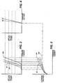
- Fig 2 is a graph of power and current for three temperatures.
- Fig 3 is a graph of voltage and current for three temperatures.
- Fig 4 is a graph of power and voltage.
- Fig 5 is a schematic diagram of the circuit.
- Fig 6 is a timing diagram.
- the circuit described herein uses a current driver for the laser which contributes to high speed and wide bandwidth, and uses the voltage drop across the diode as a measure of the diode output power.
- the result is an automatic power control circuit having fast speed and wide bandwidth operation while retaining a superior light level control and temperature compensation.
- Fig 2 shows the relationship between output power and current at three temperatures. There is a large variaton in output power as the temperature varies with constant current.
- Fig 3 shows the relationship between voltage and current, and from Figs 2 and 3, the data relating power and voltage can be extracted and plotted, as shown in Fig 4. Notice that for a constant voltage in Fig 4, there is less variation in power than there is for the constant current of Fig 2.
- This invention uses current drivers to achieve high speed performance, but uses voltage as the key parameter to control the power output level, resulting in good power level control and minimum sensitivity to temperature variations.
- the desired power is set to a predetermined level and the power output is monitored.
- the difference between the predetermined level and the actual power, as detected by a photodetector, is fed back to control the voltage, and that voltage is then used to control the current, so that the power matches the required level.
- the detector is outside of the active region, before the start of scan, so the sample rate is once per scan. The problem which remains is how to compensate for temperature variations, resulting from long strings of ON or OFF bits, that occur within the scan.
- the circuit described herein is shown in Fig 1.
- the outer loop which calibrates the power level once per scan line, consists of the laser diode 10, the output of which is shown as a dotted line.
- the power is detected by a photo detector 17 and amplified by amplifier 16.
- the dc level of the output of this amplifier is offset by amplifier 15 and the result is applied to sample-and-hold device 14 which provides one input to the summing junction 13.
- the other junction input is the predetermined level that the laser should be set to.
- the output of the summing junction 13 is the final correction voltage which is applied to the inner loop, as described below. This correction is made once each scan.
- the inner loop in this circuit is designed to regulate the laser during the scan.
- the voltage across the laser 10 is sampled by the voltage-to-current converter 18, the output of which is applied to a second summing junction 12 which adds this correction current to the one generated by the outer loop at the output of the first summing junction 13.
- the sum of both correction currents is then applied to the current generator 11 which drives the laser 10.
- the inner loop thus minimizes any laser output drift between light output (outer loop) calibrations.
- FIGs 5 and 6 A schematic diagram of one embodiment and a timing diagram for it are shown in Figs 5 and 6, the complete circuit comprising an inner and outer loop.
- the outer loop serves two purposes. The first is to calibrate the laser diode voltage to the output laser. This is accomplished by sampling the laser power using a scan detector. The detector is exposed to a full-on power level every scanline. As the detector is exposed to this light level, a sample and hold circuit samples the corresponding forward laser voltage. This sampled voltage level is used as a reference for the inner loop in between scanlines. For a multiple beam light source, the same concept applies except that time domain multiplexing may be required to sample the two beam intensity levels independently and as isolated cases.
- the second is to regulate and vary the light intensity level as requested by the exposure signal.
- the system power requirement is represented by an analog exposure level signal. Based on the exposure level presented to it, the driver adjusts the current drive level such that the exposure level requested is matched by the power output.
- the inner loop serves a single purpose. It uses the laser voltage as its reference and regulates the forward voltage drop across the laser to that level.
- This inner loop may be implemented in different ways, the essence of the circuit is that the voltage drop across the laser is monitored and the driver current level adjusted to achieve a constant voltage drop across the diode.
- Fig 6 is the timing diagram illustrating the sequence of events. Not shown in this diagram is that the laser OFF current is determined by the exposure control setup or any other means of adjustment. This setup determines the OFF power level that the ROS can tolerate without significant loss of contrast. As the scan detector samples the laser OFF power level, a sample of the laser voltage is taken and held as reference for the desired OFF level voltage within the scanline (in between scan detector samples). After the OFF level reference voltage has been established, an ON level is presented by the exposure signal. The same routine is carried out to capture an equivalent voltage level across the diode for the full ON level.
- the laser power levels are regulated by the indirect method of regulating the laser voltage drop. Any error from the corresponding set points in the forward voltage drop across the diode is compensated for by increasing or decreasing the diode current drive. Since the power and voltage drop are tracking phenomenon in a laser diode, the result is a well regulated and temperature compensated power output.
- Fig 6 there is shown a window during which the scan detector is exposed, and the timing of the laser sample, which is used in the outer loop.
- a sequence of video data comprising six pixels that are all ON, six that are OFF and six more that are ON.
- the inner loop exposes the voltage detector to the laser power during these ON and OFF periods.
- Fig 5 is the detailed diagram of the circuit.
- the laser 10 is controlled by an outer loop consisting of a light detector 17, the output signal of which is amplified in amplifier 16, sampled by sample and hold circuit 14 and applied to the summing junction 13 along with the predetermined exposure signal .
- the output of the summing junction 13 is amplified 20 and applied to the inner loop summing junction 12.
- amplifier 23 samples the voltage across the laser 10. When the laser is fully ON, the amplifier 23 output is applied through sample-and-hold 22 and amplifier 21 to the positive input of the inner junction 12. When the laser is fully Off, the amplifier 23 output is applied through sample-and-hold 24 and amplifier 26 to the negative input of the inner junction 12, the output of which is used to drive the current generator 11.
Landscapes
- Physics & Mathematics (AREA)
- Condensed Matter Physics & Semiconductors (AREA)
- General Physics & Mathematics (AREA)
- Electromagnetism (AREA)
- Optics & Photonics (AREA)
- Semiconductor Lasers (AREA)
Description
- A temperature tracking circuit for driving a laser diode incorporating an inner loop which includes a light level detector for regulating the laser diode forward voltage, and a voltage-to-current converter for driving the laser.
- A laser diode is typically set to its correct operating levels outside of the active scan region, but during active scan, the temperature of the laser can vary depending on the momentary duty cycles. For example, after long string of "ON" or "OFF" pixels, the instantaneous temperature of the diode may rise or fall, and the output light intensity (power) may vary.
- If the laser is being driven by a voltage source, the laser is self-correcting to some extent. That is, the variation in laser temperature is accompanied by a change in output power, as well as a change in forward voltage drop. In laser diodes these two parameters track well. However, the problem with a voltage source is that it is sensitive to the capacitative elements of the laser, and is not a driver of choice in high data rate systems.
- A current driver is the driver of choice that enables high data rates; however, the current drive and the Laser output power do not track as well as voltage to power. An optimum design will have to incorporate the high bit rate capability of the current drive while retaining the inherent advantage of voltage and power tracking with temperature.
- This circuit senses the power output of the laser, and uses it to drive a voltage source. However, a voltage-to-current converter is interposed between the voltage source and the laser. Thus, the resultant circuit has the advantages of both prior art circuits. Namely, the laser is driven by a current source, but the loop is regulated to a voltage, thereby achieving the best characteristics of both circuits.
- Fig 1 is a block diagram of the circuit.
- Fig 2 is a graph of power and current for three temperatures.
- Fig 3 is a graph of voltage and current for three temperatures.
- Fig 4 is a graph of power and voltage.
- Fig 5 is a schematic diagram of the circuit.
- Fig 6 is a timing diagram.
- The circuit described herein uses a current driver for the laser which contributes to high speed and wide bandwidth, and uses the voltage drop across the diode as a measure of the diode output power. The result is an automatic power control circuit having fast speed and wide bandwidth operation while retaining a superior light level control and temperature compensation.
- Fig 2 shows the relationship between output power and current at three temperatures. There is a large variaton in output power as the temperature varies with constant current. Fig 3 shows the relationship between voltage and current, and from Figs 2 and 3, the data relating power and voltage can be extracted and plotted, as shown in Fig 4. Notice that for a constant voltage in Fig 4, there is less variation in power than there is for the constant current of Fig 2.
- The highly defined threshold voltage and the relatively low temperature sensitivity of output power in Fig 4 suggests a voltage driver circuit would be desirable. However, voltage drivers have speed constraints that render them less attractive than current drivers, especially in high speed applications.
- This invention uses current drivers to achieve high speed performance, but uses voltage as the key parameter to control the power output level, resulting in good power level control and minimum sensitivity to temperature variations.
- The desired power is set to a predetermined level and the power output is monitored. The difference between the predetermined level and the actual power, as detected by a photodetector, is fed back to control the voltage, and that voltage is then used to control the current, so that the power matches the required level. The detector is outside of the active region, before the start of scan, so the sample rate is once per scan. The problem which remains is how to compensate for temperature variations, resulting from long strings of ON or OFF bits, that occur within the scan.
- The circuit described herein is shown in Fig 1. The outer loop, which calibrates the power level once per scan line, consists of the
laser diode 10, the output of which is shown as a dotted line. The power is detected by aphoto detector 17 and amplified byamplifier 16. The dc level of the output of this amplifier is offset byamplifier 15 and the result is applied to sample-and-hold device 14 which provides one input to thesumming junction 13. The other junction input is the predetermined level that the laser should be set to. The output of thesumming junction 13 is the final correction voltage which is applied to the inner loop, as described below. This correction is made once each scan. - The problem with correcting the laser power once per scan, typically either before or at the start of scan, is that during the scan, a long string of ON pixels may drive up the temperature of the laser. In the worst case, laser damage may result. For this reason, some designs gradually lower the power of the laser as time accumulates since the last calibration.
- The inner loop in this circuit is designed to regulate the laser during the scan. The voltage across the
laser 10 is sampled by the voltage-to-current converter 18, the output of which is applied to asecond summing junction 12 which adds this correction current to the one generated by the outer loop at the output of thefirst summing junction 13. The sum of both correction currents is then applied to thecurrent generator 11 which drives thelaser 10. The inner loop thus minimizes any laser output drift between light output (outer loop) calibrations. - A schematic diagram of one embodiment and a timing diagram for it are shown in Figs 5 and 6, the complete circuit comprising an inner and outer loop.
- The outer loop serves two purposes. The first is to calibrate the laser diode voltage to the output laser. This is accomplished by sampling the laser power using a scan detector. The detector is exposed to a full-on power level every scanline. As the detector is exposed to this light level, a sample and hold circuit samples the corresponding forward laser voltage. This sampled voltage level is used as a reference for the inner loop in between scanlines. For a multiple beam light source, the same concept applies except that time domain multiplexing may be required to sample the two beam intensity levels independently and as isolated cases.
- The second is to regulate and vary the light intensity level as requested by the exposure signal. Typically, the system power requirement is represented by an analog exposure level signal. Based on the exposure level presented to it, the driver adjusts the current drive level such that the exposure level requested is matched by the power output.
- The inner loop serves a single purpose. It uses the laser voltage as its reference and regulates the forward voltage drop across the laser to that level. This inner loop may be implemented in different ways, the essence of the circuit is that the voltage drop across the laser is monitored and the driver current level adjusted to achieve a constant voltage drop across the diode.
- Fig 6 is the timing diagram illustrating the sequence of events. Not shown in this diagram is that the laser OFF current is determined by the exposure control setup or any other means of adjustment. This setup determines the OFF power level that the ROS can tolerate without significant loss of contrast. As the scan detector samples the laser OFF power level, a sample of the laser voltage is taken and held as reference for the desired OFF level voltage within the scanline (in between scan detector samples). After the OFF level reference voltage has been established, an ON level is presented by the exposure signal. The same routine is carried out to capture an equivalent voltage level across the diode for the full ON level.
- After these two points have been determined, the laser power levels are regulated by the indirect method of regulating the laser voltage drop. Any error from the corresponding set points in the forward voltage drop across the diode is compensated for by increasing or decreasing the diode current drive. Since the power and voltage drop are tracking phenomenon in a laser diode, the result is a well regulated and temperature compensated power output.
- In Fig 6, there is shown a window during which the scan detector is exposed, and the timing of the laser sample, which is used in the outer loop. Next is shown a sequence of video data comprising six pixels that are all ON, six that are OFF and six more that are ON. The inner loop exposes the voltage detector to the laser power during these ON and OFF periods.
- Fig 5 is the detailed diagram of the circuit. The
laser 10 is controlled by an outer loop consisting of alight detector 17, the output signal of which is amplified inamplifier 16, sampled by sample and holdcircuit 14 and applied to the summingjunction 13 along with the predetermined exposure signal . The output of the summingjunction 13 is amplified 20 and applied to the innerloop summing junction 12. - In the inner loop,
amplifier 23 samples the voltage across thelaser 10. When the laser is fully ON, theamplifier 23 output is applied through sample-and-hold 22 andamplifier 21 to the positive input of theinner junction 12. When the laser is fully Off, theamplifier 23 output is applied through sample-and-hold 24 andamplifier 26 to the negative input of theinner junction 12, the output of which is used to drive thecurrent generator 11. - While the invention has been described with reference to a specific embodiment, it will be understood by those skilled in the art that various changes may be made and equivalents may be substituted for elements thereof without departing from the scope of the invention as defined in
Claim 1.
Claims (1)
- A circuit for regulating the power of the light output of a laser diode means (10) comprising:a voltage controlled current generator (11) for driving said laser means,an outer loop comprising,an inner loop comprising a voltage detector means (18) for determining the voltage across said laser means, for generating a voltage correction signal, and applying said voltage correction signal to said inner loop summing means (12) as an input to be added to said corrected power signal.a) a light detector means (16, 17) for detecting the output power of said laser means and generating a power signal,b) an outer loop summing means (13) responsive to said light detector means for comparing said power signal to a predetermined value and generating a corrected power signal, andc) an inner loop summing means (12) for coupling said corrected power signal to said current generator, and
Applications Claiming Priority (2)
| Application Number | Priority Date | Filing Date | Title |
|---|---|---|---|
| US173016 | 1993-12-27 | ||
| US08/173,016 US5414280A (en) | 1993-12-27 | 1993-12-27 | Current driven voltage sensed laser drive (CDVS LDD) |
Publications (3)
| Publication Number | Publication Date |
|---|---|
| EP0660471A2 EP0660471A2 (en) | 1995-06-28 |
| EP0660471A3 EP0660471A3 (en) | 1995-11-29 |
| EP0660471B1 true EP0660471B1 (en) | 1997-07-09 |
Family
ID=22630163
Family Applications (1)
| Application Number | Title | Priority Date | Filing Date |
|---|---|---|---|
| EP94120611A Expired - Lifetime EP0660471B1 (en) | 1993-12-27 | 1994-12-23 | Current driven voltage sensed laser diode driver (CDVS LDD) |
Country Status (4)
| Country | Link |
|---|---|
| US (1) | US5414280A (en) |
| EP (1) | EP0660471B1 (en) |
| JP (1) | JPH07202301A (en) |
| DE (1) | DE69404118T2 (en) |
Cited By (1)
| Publication number | Priority date | Publication date | Assignee | Title |
|---|---|---|---|---|
| WO2009120454A1 (en) * | 2008-02-28 | 2009-10-01 | Respiratory Management Technology | System and method for measuring the output of a photodetector |
Families Citing this family (35)
| Publication number | Priority date | Publication date | Assignee | Title |
|---|---|---|---|---|
| US5506853A (en) * | 1994-11-23 | 1996-04-09 | Harris Corporation | Offset stabilization of wide dynamic range injection laser diode with single bit sampling |
| JPH10181098A (en) * | 1996-12-26 | 1998-07-07 | Minolta Co Ltd | Electro-optical element driving apparatus |
| DE19843206A1 (en) * | 1998-09-16 | 2000-04-20 | Siemens Ag | Optical transmitter for multi-channel optical data transmission |
| JP4148485B2 (en) * | 1998-10-05 | 2008-09-10 | キヤノン株式会社 | Image forming apparatus and copying machine |
| DE19912463A1 (en) * | 1999-03-19 | 2000-09-28 | Sensor Line Ges Fuer Optoelekt | Process for stabilizing the optical output power of light-emitting diodes and laser diodes |
| US6879619B1 (en) | 1999-07-27 | 2005-04-12 | Intel Corporation | Method and apparatus for filtering an optical beam |
| US6853654B2 (en) * | 1999-07-27 | 2005-02-08 | Intel Corporation | Tunable external cavity laser |
| US6856632B1 (en) | 1999-09-20 | 2005-02-15 | Iolon, Inc. | Widely tunable laser |
| US6847661B2 (en) * | 1999-09-20 | 2005-01-25 | Iolon, Inc. | Tunable laser with microactuator |
| US7120176B2 (en) * | 2000-07-27 | 2006-10-10 | Intel Corporation | Wavelength reference apparatus and method |
| DE10042022A1 (en) * | 2000-08-08 | 2002-03-07 | Infineon Technologies Ag | Method and device for measuring the temperature of the laser-active region of a semiconductor laser diode |
| JP4123791B2 (en) * | 2001-03-05 | 2008-07-23 | 富士ゼロックス株式会社 | Light emitting element driving apparatus and light emitting element driving system |
| US7352786B2 (en) * | 2001-03-05 | 2008-04-01 | Fuji Xerox Co., Ltd. | Apparatus for driving light emitting element and system for driving light emitting element |
| US6658031B2 (en) * | 2001-07-06 | 2003-12-02 | Intel Corporation | Laser apparatus with active thermal tuning of external cavity |
| US6816516B2 (en) | 2001-03-21 | 2004-11-09 | Intel Corporation | Error signal generation system |
| US6804278B2 (en) * | 2001-07-06 | 2004-10-12 | Intel Corporation | Evaluation and adjustment of laser losses according to voltage across gain medium |
| US6901088B2 (en) | 2001-07-06 | 2005-05-31 | Intel Corporation | External cavity laser apparatus with orthogonal tuning of laser wavelength and cavity optical pathlength |
| US6822979B2 (en) | 2001-07-06 | 2004-11-23 | Intel Corporation | External cavity laser with continuous tuning of grid generator |
| US6788724B2 (en) * | 2001-07-06 | 2004-09-07 | Intel Corporation | Hermetically sealed external cavity laser system and method |
| US7230959B2 (en) * | 2002-02-22 | 2007-06-12 | Intel Corporation | Tunable laser with magnetically coupled filter |
| US6763047B2 (en) * | 2002-06-15 | 2004-07-13 | Intel Corporation | External cavity laser apparatus and methods |
| US6845121B2 (en) * | 2002-06-15 | 2005-01-18 | Intel Corporation | Optical isolator apparatus and methods |
| KR100857083B1 (en) | 2002-06-26 | 2008-09-05 | 주식회사 히타치엘지 데이터 스토리지 코리아 | Method for setting the reference power in optical disc driver |
| US7106769B2 (en) * | 2003-04-09 | 2006-09-12 | Elantec Semiconductor, Inc. | Adjustable power control for laser drivers and laser diodes |
| US7333521B1 (en) * | 2003-12-04 | 2008-02-19 | National Semiconductor Corporation | Method of sensing VCSEL light output power by monitoring electrical characteristics of the VCSEL |
| US20050180711A1 (en) * | 2004-02-13 | 2005-08-18 | Kamath Kishore K. | Dual loop automatic power control of optical transmitters |
| US7630422B1 (en) | 2005-01-14 | 2009-12-08 | National Semiconductor Corporation | Driver for vertical-cavity surface-emitting laser and method |
| US7512163B2 (en) * | 2005-10-04 | 2009-03-31 | Microsoft Corporation | Dual current control for laser diode driver circuit |
| US7642770B2 (en) * | 2007-03-16 | 2010-01-05 | Mediatek Inc. | Light-driving system capable of providing signal-measured calibration and a method for performing the same |
| US7822086B2 (en) * | 2007-07-27 | 2010-10-26 | Microvision, Inc. | Laser projection temperature compensation |
| US8450941B2 (en) | 2010-12-17 | 2013-05-28 | Intersil Americas Inc. | Systems and methods for dynamic power management for use with a video display device |
| DE102013202289B4 (en) * | 2013-02-13 | 2016-03-17 | Siemens Aktiengesellschaft | Method and arrangement for driving a wavelength-tunable laser diode in a spectrometer |
| JP6321461B2 (en) * | 2014-06-10 | 2018-05-09 | 日本オクラロ株式会社 | Semiconductor optical device and control method |
| DE102018212687A1 (en) * | 2018-07-30 | 2020-01-30 | Koninklijke Philips N.V. | Method and device for monitoring the optical output power of a laser diode with an associated photodiode and particle sensor device |
| NL2028674B1 (en) * | 2021-07-09 | 2023-01-16 | Nearfield Instr B V | Laser diode arrangement, method of operating a laser diode and scanning microscope device comprising a laser diode |
Family Cites Families (12)
| Publication number | Priority date | Publication date | Assignee | Title |
|---|---|---|---|---|
| JPS61165835A (en) * | 1985-01-17 | 1986-07-26 | Olympus Optical Co Ltd | Optical output stabilizer |
| JPS61165836A (en) * | 1985-01-17 | 1986-07-26 | Olympus Optical Co Ltd | Optical output stabilizer |
| JPS6474780A (en) * | 1987-09-17 | 1989-03-20 | Copal Electronics | Stabilization of semiconductor laser light |
| JPH06103765B2 (en) * | 1987-10-30 | 1994-12-14 | 日本電気株式会社 | Semiconductor laser bias current control method |
| JPH01214080A (en) * | 1988-02-22 | 1989-08-28 | Seiko Epson Corp | Semiconductor laser driving circuit |
| JPH0240609A (en) * | 1988-07-30 | 1990-02-09 | Ricoh Co Ltd | Output controller for laser diode |
| JPH0273682A (en) * | 1988-09-08 | 1990-03-13 | Nippon Digital Equip Kk | Laser diode driving method and device |
| JPH0399484A (en) * | 1989-09-12 | 1991-04-24 | Brother Ind Ltd | Semiconductor laser drive circuit |
| US5237858A (en) * | 1990-07-19 | 1993-08-24 | Neotec Co., Inc. | Method for determining the unhydration ratio of cement contained in cement sludge |
| US5123023A (en) * | 1990-11-21 | 1992-06-16 | Polaroid Corporation | Laser driver with plural feedback loops |
| JPH0595150A (en) * | 1991-06-28 | 1993-04-16 | Toshiba Corp | Controller for laser |
| US5187713A (en) * | 1992-01-30 | 1993-02-16 | Northern Telecom Limited | Nonlinear device control methods and apparatus |
-
1993
- 1993-12-27 US US08/173,016 patent/US5414280A/en not_active Expired - Lifetime
-
1994
- 1994-12-19 JP JP6314694A patent/JPH07202301A/en active Pending
- 1994-12-23 DE DE69404118T patent/DE69404118T2/en not_active Expired - Fee Related
- 1994-12-23 EP EP94120611A patent/EP0660471B1/en not_active Expired - Lifetime
Cited By (1)
| Publication number | Priority date | Publication date | Assignee | Title |
|---|---|---|---|---|
| WO2009120454A1 (en) * | 2008-02-28 | 2009-10-01 | Respiratory Management Technology | System and method for measuring the output of a photodetector |
Also Published As
| Publication number | Publication date |
|---|---|
| US5414280A (en) | 1995-05-09 |
| DE69404118D1 (en) | 1997-08-14 |
| EP0660471A2 (en) | 1995-06-28 |
| JPH07202301A (en) | 1995-08-04 |
| DE69404118T2 (en) | 1997-10-30 |
| EP0660471A3 (en) | 1995-11-29 |
Similar Documents
| Publication | Publication Date | Title |
|---|---|---|
| EP0660471B1 (en) | Current driven voltage sensed laser diode driver (CDVS LDD) | |
| US6559995B2 (en) | Optical transmission method and optical transmitter with temperature compensation function | |
| US6292497B1 (en) | Laser diode driving method and circuit | |
| US7352786B2 (en) | Apparatus for driving light emitting element and system for driving light emitting element | |
| US5018154A (en) | Semiconductor laser drive device | |
| CA1085462A (en) | Automatic bias control circuit for injection lasers | |
| US4817098A (en) | Semiconductor laser driver system | |
| US5237579A (en) | Semiconductor laser controller using optical-electronic negative feedback loop | |
| US6982689B2 (en) | Light-emitting element drive apparatus | |
| US7480320B2 (en) | Semiconductor laser driving device, semiconductor laser driving method, and image forming apparatus using semiconductor laser driving device | |
| US4771431A (en) | Semiconductor laser drive | |
| EP0507298A2 (en) | Laser scanner control circuit which is used in image forming apparatus and driver IC for use in such a circuit | |
| US5978124A (en) | Light emitting control apparatus and optical transmitter | |
| US5313482A (en) | Method and circuit arrangement for correcting the light power output of a laser diode | |
| US4868675A (en) | Control circuit for a laser printer | |
| JPH06103765B2 (en) | Semiconductor laser bias current control method | |
| US5479425A (en) | Thermal compensation of injection laser diodes driven by shunt current modulations | |
| JPH10276048A (en) | Offset compensation circuit | |
| US5506853A (en) | Offset stabilization of wide dynamic range injection laser diode with single bit sampling | |
| JPH01106667A (en) | Laser recorder | |
| JPS6152042A (en) | Semiconductor laser driver | |
| JP3042951B2 (en) | Light quantity stabilizing device in image input device | |
| JPH07119120B2 (en) | Laser output control circuit | |
| JPH0784069B2 (en) | Driving device for semiconductor laser | |
| JPH07111355A (en) | Optical transmitter |
Legal Events
| Date | Code | Title | Description |
|---|---|---|---|
| PUAI | Public reference made under article 153(3) epc to a published international application that has entered the european phase |
Free format text: ORIGINAL CODE: 0009012 |
|
| AK | Designated contracting states |
Kind code of ref document: A2 Designated state(s): DE FR GB |
|
| PUAL | Search report despatched |
Free format text: ORIGINAL CODE: 0009013 |
|
| AK | Designated contracting states |
Kind code of ref document: A3 Designated state(s): DE FR GB |
|
| 17P | Request for examination filed |
Effective date: 19960528 |
|
| GRAG | Despatch of communication of intention to grant |
Free format text: ORIGINAL CODE: EPIDOS AGRA |
|
| 17Q | First examination report despatched |
Effective date: 19960822 |
|
| GRAH | Despatch of communication of intention to grant a patent |
Free format text: ORIGINAL CODE: EPIDOS IGRA |
|
| GRAH | Despatch of communication of intention to grant a patent |
Free format text: ORIGINAL CODE: EPIDOS IGRA |
|
| GRAA | (expected) grant |
Free format text: ORIGINAL CODE: 0009210 |
|
| AK | Designated contracting states |
Kind code of ref document: B1 Designated state(s): DE FR GB |
|
| REF | Corresponds to: |
Ref document number: 69404118 Country of ref document: DE Date of ref document: 19970814 |
|
| ET | Fr: translation filed | ||
| PLBE | No opposition filed within time limit |
Free format text: ORIGINAL CODE: 0009261 |
|
| STAA | Information on the status of an ep patent application or granted ep patent |
Free format text: STATUS: NO OPPOSITION FILED WITHIN TIME LIMIT |
|
| 26N | No opposition filed | ||
| REG | Reference to a national code |
Ref country code: GB Ref legal event code: IF02 |
|
| PGFP | Annual fee paid to national office [announced via postgrant information from national office to epo] |
Ref country code: FR Payment date: 20021210 Year of fee payment: 9 |
|
| PGFP | Annual fee paid to national office [announced via postgrant information from national office to epo] |
Ref country code: GB Payment date: 20021218 Year of fee payment: 9 |
|
| PGFP | Annual fee paid to national office [announced via postgrant information from national office to epo] |
Ref country code: DE Payment date: 20021231 Year of fee payment: 9 |
|
| PG25 | Lapsed in a contracting state [announced via postgrant information from national office to epo] |
Ref country code: GB Free format text: LAPSE BECAUSE OF NON-PAYMENT OF DUE FEES Effective date: 20031223 |
|
| PG25 | Lapsed in a contracting state [announced via postgrant information from national office to epo] |
Ref country code: DE Free format text: LAPSE BECAUSE OF NON-PAYMENT OF DUE FEES Effective date: 20040701 |
|
| GBPC | Gb: european patent ceased through non-payment of renewal fee |
Effective date: 20031223 |
|
| PG25 | Lapsed in a contracting state [announced via postgrant information from national office to epo] |
Ref country code: FR Free format text: LAPSE BECAUSE OF NON-PAYMENT OF DUE FEES Effective date: 20040831 |
|
| REG | Reference to a national code |
Ref country code: FR Ref legal event code: ST |