EP0654712B1 - Method for forming thin film pattern - Google Patents
Method for forming thin film pattern Download PDFInfo
- Publication number
- EP0654712B1 EP0654712B1 EP94115231A EP94115231A EP0654712B1 EP 0654712 B1 EP0654712 B1 EP 0654712B1 EP 94115231 A EP94115231 A EP 94115231A EP 94115231 A EP94115231 A EP 94115231A EP 0654712 B1 EP0654712 B1 EP 0654712B1
- Authority
- EP
- European Patent Office
- Prior art keywords
- thin film
- sol
- film pattern
- pattern
- polysilane
- Prior art date
- Legal status (The legal status is an assumption and is not a legal conclusion. Google has not performed a legal analysis and makes no representation as to the accuracy of the status listed.)
- Expired - Lifetime
Links
Images
Classifications
-
- G—PHYSICS
- G03—PHOTOGRAPHY; CINEMATOGRAPHY; ANALOGOUS TECHNIQUES USING WAVES OTHER THAN OPTICAL WAVES; ELECTROGRAPHY; HOLOGRAPHY
- G03F—PHOTOMECHANICAL PRODUCTION OF TEXTURED OR PATTERNED SURFACES, e.g. FOR PRINTING, FOR PROCESSING OF SEMICONDUCTOR DEVICES; MATERIALS THEREFOR; ORIGINALS THEREFOR; APPARATUS SPECIALLY ADAPTED THEREFOR
- G03F7/00—Photomechanical, e.g. photolithographic, production of textured or patterned surfaces, e.g. printing surfaces; Materials therefor, e.g. comprising photoresists; Apparatus specially adapted therefor
- G03F7/26—Processing photosensitive materials; Apparatus therefor
- G03F7/265—Selective reaction with inorganic or organometallic reagents after image-wise exposure, e.g. silylation
-
- G—PHYSICS
- G03—PHOTOGRAPHY; CINEMATOGRAPHY; ANALOGOUS TECHNIQUES USING WAVES OTHER THAN OPTICAL WAVES; ELECTROGRAPHY; HOLOGRAPHY
- G03F—PHOTOMECHANICAL PRODUCTION OF TEXTURED OR PATTERNED SURFACES, e.g. FOR PRINTING, FOR PROCESSING OF SEMICONDUCTOR DEVICES; MATERIALS THEREFOR; ORIGINALS THEREFOR; APPARATUS SPECIALLY ADAPTED THEREFOR
- G03F7/00—Photomechanical, e.g. photolithographic, production of textured or patterned surfaces, e.g. printing surfaces; Materials therefor, e.g. comprising photoresists; Apparatus specially adapted therefor
-
- G—PHYSICS
- G03—PHOTOGRAPHY; CINEMATOGRAPHY; ANALOGOUS TECHNIQUES USING WAVES OTHER THAN OPTICAL WAVES; ELECTROGRAPHY; HOLOGRAPHY
- G03F—PHOTOMECHANICAL PRODUCTION OF TEXTURED OR PATTERNED SURFACES, e.g. FOR PRINTING, FOR PROCESSING OF SEMICONDUCTOR DEVICES; MATERIALS THEREFOR; ORIGINALS THEREFOR; APPARATUS SPECIALLY ADAPTED THEREFOR
- G03F7/00—Photomechanical, e.g. photolithographic, production of textured or patterned surfaces, e.g. printing surfaces; Materials therefor, e.g. comprising photoresists; Apparatus specially adapted therefor
- G03F7/004—Photosensitive materials
- G03F7/075—Silicon-containing compounds
- G03F7/0754—Non-macromolecular compounds containing silicon-to-silicon bonds
Definitions
- the present invention relates to a method for forming a thin film pattern on a substrate. More particularly, it relates to a method for patterning a functional ceramic thin film formed by means of a sol-gel processing.
- a method for synthesizing a ceramic thin film using a solution reaction (referred to as a "sol-gel processing") has attracted special interest recently.
- the sol-gel processing is a method comprising synthesizing an inorganic polymer precursor from an organic metal compound or a metal complex in a solution by using a hydrolysis reaction or condensation reaction; applying the solution on a substrate by means of a spray method, dipping method or spin-coating method to form a thin film; and subjecting the thin film to a heat treatment to form a functional ceramic thin film.
- the functional ceramic thin film is used as dielectric film, insulator film, protective film, etc.
- the sol-gel processing is applied for the surface treatment of functional glass or plastic, for example, anti-diffusion film of alkali, interference colored film, anti-reflection film, reflection film and the like.
- the method for forming a thin film by means of the sol-gel processing has excellent characteristics such as temperature reduction of process temperature, freedom of composition, formation of uniform thin film on substrate having large surface area and the like.
- the present inventors have already proposed a process for dyeing a pattern using a silanol group produced by exposing an organic polysilane to ultraviolet light (Japanese Laid-Open Patent Publication No. 05-188215) and a method for coloring a pattern by dipping in a colored sol solution comprising a metal alkoxide containing a dye or a pigment as a raw material (Japanese Patent Application No. 4-68243). Further, the present inventors have further studied to develop a function other than a colored pattern using a sol.
- the main object of the present invention is to provide a method for forming a thin film pattern having excellent accuracy of pattern, which improves a method for forming a thin film by means of the sol-gel processing and which enables manufacturing at low cost.
- the present invention provides a method for forming a thin film pattern, which comprises the steps of:
- this method further comprises the step of removing the part other than the ultraviolet light-exposed part of the polysilane layer, after the thin film pattern was formed.
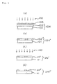
- Figs. 1(a) to (d) are schematic diagrams illustrating one embodiment of the steps of forming a thin film pattern of the present invention.
- metal oxide sol used herein means those which are prepared by subjecting one or more sorts of metals to condensation polymerization through oxygen and solating in a suitable solvent.
- the resulting sol is referred to as a silica sol.
- Polysilane used in the present invention is a polysilane having a structure of the formula: wherein R 1 , R 2 , R 3 and R 4 indicate a group which is independently selected from the group consisting of a substituted or non-substituted aliphatic hydrocarbon residue such as methyl group, n-propyl group, n-butyl group, n-hexyl group, phenylmethyl group, trifluoropropyl group and nonafluorohexyl group, an aromatic hydrocarbon residue such as p-tolyl group, biphenyl group and phenyl group and a substituted or non-substituted alicyclic hydrocarbon residue such as cyclohexyl group and methylcyclohexyl group; and m and n indicate an integer.
- the number of a carbon atom is 1 to 10.
- a kind of the substituents R 1 to R 4 having 6 to 14 carbon atoms and the value of m and n are not particularly important and this polysilane resin may have organic solvent-solubility and can be coated to form an uniform film (film thickness of 0.1 to 10 ⁇ m).
- a polysilane layer is firstly formed on a suitable substrate.
- the substrate its shape and material are not specifically limited. Glass plate, metal plate, plastic plate can be used according to the application.
- the polysilane layer is formed on such a substrate.
- the formation method may be any one which can form a polysilane layer having an uniform thickness and is not specifically limited.
- a spin-coating method is normally used.
- the organic solvent used in the step of forming the polysilane layer may be any solvent which can dissolve polysilane and is not specifically limited. Toluene is suitably used in this method. It is preferred that the dry film thickness of the polysilane layer is within a range from 0.1 to 10 ⁇ m.
- FIG. 1 (a) to (d) One embodiment of the steps of forming a thin film pattern is shown in Figs. 1 (a) to (d).
- ultraviolet light is irradiated to a laminate 104 for forming pattern thin film comprising a substrate 101 and a polysilane layer 102 thus obtained, using an ultraviolet light source such as mercury vapor lamp according to the pattern.
- Ultraviolet light 110 is irradiated through a pattern mask 103 put on the laminate 104 for forming thin film.
- Ultraviolet light used in the present invention has a wavelength of 250 to 400 nm as a ⁇ - ⁇ ' absorption range of polysilane.
- irradiation may be conducted at a light energy of 0.5 to 10 J/cm 2 per 1 ⁇ m in thickness of the polysilane layer.
- Si-Si bond which exists in the polysilane layer is decomposed by ultraviolet light irradiation to form Si-OH (silanol group). Accordingly, a latent image containing a silanol group is formed in the irradiated laminate for forming thin film according to the pattern.
- a sol was absorbed at the pattern part of the laminate for forming thin film.
- water-soluble organic solvents such as acetonitrile, dioxane, tetrahydrofuran, etc. may be added to the metal oxide sol, if necessary,
- a water-soluble organic solvent may be formulated in the sol solution in an amount of 1 to 30% by weight.
- absorption of the sol is suitably conducted by dipping a thin film-forming material in the sol solution maintained at 20 to 40°C for 1 to 40 minutes.
- the material of the metal oxide sol there can be normally used materials used in the sol-gel processing.
- the kind of the metal varies depending on the objective function, but examples of the material include metal organic substances (e.g. alkoxide, acetylacetonate, acetate, amine, etc.), soluble inorganic salts (e.g. nitrate, etc.) or dispersants of fine oxide particles of metals (e.g. Si, Zr, Pb, Ti, Ba, Sr, Nb, K, Li, Ta, In, Sn, Zn, Y, Cu, Ca, Mn, Fe, Co, La, Al, Mg, V, etc.).
- metal organic substances e.g. alkoxide, acetylacetonate, acetate, amine, etc.
- soluble inorganic salts e.g. nitrate, etc.
- dispersants of fine oxide particles of metals e.g. Si, Zr, Pb, Ti, Ba, Sr,
- a solution which is solated by subjecting to the condensation polymerization reaction using a catalyst such as acid or base.
- a catalyst such as acid or base.
- all substituents of the metal may not be converted into a condensation-polymerizable functional group, but a part of an organic functional group may be remained. Further, materials which can dissolve or disperse in the sol solution may be added.
- tetraethoxysilane is hydrolyzed and condensed with dehydrating by dissolving it in a mixed solution of ethanol and water and adding hydrochloric acid to the mixture, followed by stirring at room temperature for 2 hours to give a homogeneous silica sol.
- composition of the silica sol is preferably composed of 50 to 200 parts by weight of ethanol, 1 to 200 parts by weight of water and 0.1 to 3 parts by weight of hydrochloric acid, based on 100 parts by weight of tetraethoxysilane. If necessary, water-soluble organic solvents such as acetonitrile, dioxane, tetrahydrofuran, etc. may be further added.
- the metal oxide sol is absorbed at the ultraviolet light-irradiated part of the polysilane layer and incorporated into the interior of the polysilane layer. It is considered that absorption proceeds into the interior through a fine hole which exists in the ultraviolet light-irradiated part of the polysilane layer.
- the diameter of sol particles is several nm to about sixty nm and they can be sticked with diffusing. It was confirmed that a particulate material having a suitable size which coexists with sol particles can be diffused together with sol particles into the interior, similar to the case that sol particles exist alone.
- two or more sorts of them may be used in combination to develop a function.
- Examples of the functional atom include fluorine. Water repellency due to fluorine can be imparted on the polysilane layer by forming a sol containing a lot of fluorine atoms and absorbing the sol on the polysilane layer.
- Examples of the functional group used in such a method include hydrophobic groups (e.g. alkyl group, etc.), ion-exchange groups (e.g. carboxyl group, sulfo group, acidic hydroxyl group, amino group, etc) and the like.
- the particulate material includes copper and silver particles.
- the particulate material may be dispersed using the silica sol, or the particulate material may be once dispersed using a nonionic surfactant and then mixed when the silica sol is prepared.
- the particle size exceeds 500 nm, particles can not be diffused into the ultraviolet light-irradiated part of polysilane even if they are dipped in the sol solution and, therefore, they can not be sticked.
- the particle size can be measured by a normal centrifugal sedimentation method. It is considered that silica sol particles are adsorbed on the surface of the particulate material.
- Adsorption of the silica sol on the surface of particles can be easily confirmed by measuring a zeta potential.
- the zeta potential of the material which was dispersed using the nonionic surfactant is dispersed becomes stable at -5 to -25 mV because the silanol group came into existence on the surface by absorption of the silica sol.
- the material which can dissolve in the sol solution may be any organic polymer material which dissolves in water or alcohol and which interacts with the silanol group of the silica sol, and it can be diffused into the ultraviolet light-irradiated part of the polysilane layer together with sol particles and sticked.
- Suitable examples of the polymeric material include polymers containing an alcoholic hydroxyl group (e.g. polyvinyl alcohol, polyethylene glycol, cellulose, etc.), and polymers containing an amide group (e.g. poly(2-methyl-2-oxazoline), poly(N-vinylpyrrolidone), poly(N,N-dimethylacrylamide)).
- the laminate for forming thin film in which a sol was absorbed at the pattern part is dried after the sol solution was removed.
- a method of removing the sol solution there can be used a method of washing with water or a method of blowing off by an air blow.
- drying is conducted at not less than 100°C for 30 minutes to 2 hours.
- an organic substituent is eliminated by heating at not less than 400°C to give a metal oxide thin film.
- a laminate 104' for forming thin film in which a desired pattern is formed By a thin film pattern-forming step, as shown in Fig. 1(b), a laminate 104' for forming thin film in which a desired pattern is formed.
- an irregular pattern thin film as shown in Fig. 1 (d) can be obtained by exposing the total surface to ultraviolet light as shown in Fig. 1(c) and decomposing the residual polysilane layer to remove.
- a method of removing an unnecessary polysilane layer there can be used a method of volatilizing by heating and a method of removing with a solvent.
- the polysilane layer is removed by heating, it is sufficient to heat at not less than 200°C for 10 to 60 minutes. In this case, sol particles may have no functional characteristics.
- a thin film having a different function can be easily patterned on the same substrate by changing the part to be exposed to ultraviolet light and repeating the steps of Figs. 1(a) and (b) using a sol solution of a different formulation.
- a photolithographic step using a resist which is necessary for patterning is not required in the method for forming a thin film pattern of the present invention.
- a pattern thin film formed by this method can be selected according to the required function because it can form a flat layer having no irregularity unless the polysilane layer of the non-exposed part is removed, or it can form a pattern thin film having irregularity if the polysilane layer of the non-exposed part is removed.
- the patterning can form a fine pattern thin film having resolution of "submicron order" because of high resolution of photocomposition of the polysilane layer, so that, it is suitable for processing of the irregular surface having high density in comparison with a stamper method.
- the area of applicability of this technique is wide and a thin film patterning having various functions can be made by selecting the kind of the substrate and the sol material.
- a particle size of this paste dispersion was measured using a (centrifugal sedimentation method) particle size measuring equipment (CAPA-700, manufactured by Horiba, Ltd.). As a result, the average particle size was 150 nm.
- polyethylene glycol 6000 having an average molecular weight of 6000 manufactured by Wako Pure Chemical industries, Ltd.
- 13 g of tetraethoxysilane, 20 g of ethanol and 13 g of water were charged in a beaker and 0.1 g of concentrated hydrochloric acid was added with stirring, and the mixture was stirred at 30°C for 2 hours to prepare a sol, to which were further added 38 g of water and 10 g of acetonitrile to give a polyethylene glycol-containing silica sol for dipping.
- a 10% toluene solution of polysilane obtained in Preparation Example 1 was applied on a glass substrate (5 cm x 5 cm x 0.11 cm in thickness) using a spin coater ("PRS-14", manufactured by Dynapart Co.) so that the dry film thickness may become 2 ⁇ m.
- a quartz photomask was put on the resulting laminate for forming thin film pattern which was exposed to ultraviolet light at a light energy of 4 J/cm 2 using an ultra-high pressure mercury lamp parallel exposure equipment (CL-50-200A, manufactured by Japan Storage Battery Co., Ltd.). After the photomask was removed, the laminate in which a latent image was formed was dipped in a sol obtained in Preparation Example 2 for 5 minutes. After dipping, the laminate was washed with water and dried at 200°C for 30 minutes to give a pattern thin film of a fluorine silica gel.
- a surface contact angle of this fluorine silica gel to the thin film pattern part was measured using a contact angle measuring equipment (CA-Z type, manufactured by Kyowa Kaimen Kagaku Co., Ltd.). As a result, it was 96°. Further, a contact angle of the non-exposed part of the polysilane layer was measured. As a result, it was 90°. Further, ultraviolet light was irradiated on this laminate for forming thin film pattern at a light energy of 4 J/cm 2 using the above equipment and the laminate was dried at 160°C for 30 minutes. As a result, the contact angle of the pattern part of the fluorine silica gel became 98°, but the contact angle of the non-sticked part of the gel thin film was further decreased to 80°.
- CA-Z type manufactured by Kyowa Kaimen Kagaku Co., Ltd.
- Aqueous ink for flexography (Aqua PAC92 India ink, manufactured by Toyo Ink Co., Ltd.) was applied on this laminate for forming thin film pattern.
- the pattern part in which the fluorine silica gel thin film was formed repelled ink.
- a 15% toluene solution of polysilane obtained in Preparation Example 1 was applied on a glass substrate (5 cm x 5 cm x 0.11 cm in thickness) using a spin coater ("PRS-14", manufactured by Dynapart Co.) so that the dry film thickness may become 5 ⁇ m.
- PRS-14 manufactured by Dynapart Co.
- a quartz photomask was put on the resulting laminate for forming thin film pattern which was exposed to ultraviolet light at a light energy of 10 J/cm 2 using an ultra-high pressure mercury lamp parallel exposure equipment (CL-50-200A, manufactured by Japan Storage Battery Co., Ltd.). After the photomask was removed, the laminate in which a latent image was formed was dipped in a sol obtained in Preparation Example 3 for 5 minutes.
- the laminate was washed with water and calcinated at 600°C for 30 minutes to give a conductive pattern thin film of silicon oxide containing silver particles. A resistance value of this conductive film was measured. As a result, the film had a volume resistance value of 10 -2 ⁇ cm. Thus, it is possible to form a pattern of a conductive thin film on an insulation substrate by a simple method.
- a 15% toluene solution of polysilane obtained in Preparation Example 1 was applied on a glass substrate (5 cm x 5 cm x 0.11 cm in thickness) using a spin coater ("PRS-14", manufactured by Dynapart Co.) so that the dry film thickness may become 5 ⁇ m.
- PRS-14 manufactured by Dynapart Co.
- a quartz photomask was put on the resulting laminate for forming thin film pattern which was exposed to ultraviolet light having at a light energy of 10 J/cm 2 using an ultra-high pressure mercury lamp parallel exposure equipment (CL-50-200A, manufactured by Japan Storage Battery Co., Ltd.). After the photomask was removed, the laminate on which a latent image was formed was dipped in a sol obtained in Preparation Example 5 for 5 minutes.
- the laminate was washed with water and calcinated at 600°C for 30 minutes. However, no sticking of silver particles was observed. Thus, sticking of particles having a particle size of more than 500 nm can not be conducted because the particles can not be diffused into the ultraviolet light-irradiated part of the polysilane layer.
- a 15% toluene solution of polysilane obtained in Preparation Example 1 was applied on a glass substrate (5 cm x 5 cm x 0.11 cm in thickness) using a spin coater ("PRS-14", manufactured by Dynapart Co.) so that the dry film thickness may become 5 ⁇ m.
- PRS-14 manufactured by Dynapart Co.
- a quartz photomask was put on the resulting laminate for forming thin film pattern which was exposed to ultraviolet light at a light energy of 10 J/cm 2 using an ultra-high pressure mercury lamp parallel exposure equipment (CL-50-200A, manufactured by Japan Storage Battery.). After the photomask was removed, the laminate on which a latent image was formed was dipped in a sol obtained in Preparation Example 4 for 5 minutes.
- the laminate was washed with water and dried at 200°C for 30 minutes to give a pattern thin film of a silica gel containing polyethylene glycol. Further, this pattern thin film was completely decomposed by calcinating at 600°C for one hour to give a porous body having fine pores. The porosity distribution of this porous body was calculated by a nitrogen gas method. As a result, the porous body had a pore of about 20 ⁇ in diameter. Thus, it is possible to form a pattern of a porous thin film by a simple method.
Landscapes
- Physics & Mathematics (AREA)
- General Physics & Mathematics (AREA)
- Organic Chemistry (AREA)
- Chemical & Material Sciences (AREA)
- Chemical Kinetics & Catalysis (AREA)
- Inorganic Chemistry (AREA)
- Spectroscopy & Molecular Physics (AREA)
- Photosensitive Polymer And Photoresist Processing (AREA)
- Chemically Coating (AREA)
- Application Of Or Painting With Fluid Materials (AREA)
- Exposure And Positioning Against Photoresist Photosensitive Materials (AREA)
- Manufacturing Of Printed Wiring (AREA)
- Silicon Polymers (AREA)
Description
- The present invention relates to a method for forming a thin film pattern on a substrate. More particularly, it relates to a method for patterning a functional ceramic thin film formed by means of a sol-gel processing.
- A method for synthesizing a ceramic thin film using a solution reaction (referred to as a "sol-gel processing") has attracted special interest recently. The sol-gel processing is a method comprising synthesizing an inorganic polymer precursor from an organic metal compound or a metal complex in a solution by using a hydrolysis reaction or condensation reaction; applying the solution on a substrate by means of a spray method, dipping method or spin-coating method to form a thin film; and subjecting the thin film to a heat treatment to form a functional ceramic thin film. The functional ceramic thin film is used as dielectric film, insulator film, protective film, etc. in electronic devices such as thin film capacitor, LSI, electroluminescent device and the like, and the formation technique by means of the sol-gel processing has been studied intensively. On the other hand, in addition to the above electronic devices, the sol-gel processing is applied for the surface treatment of functional glass or plastic, for example, anti-diffusion film of alkali, interference colored film, anti-reflection film, reflection film and the like.
- The method for forming a thin film by means of the sol-gel processing has excellent characteristics such as temperature reduction of process temperature, freedom of composition, formation of uniform thin film on substrate having large surface area and the like.
- However, there is no method of patterning a thin film, and a method of removing a thin film by conducting etching after formation of the thin film is popular. A complicated lithography step using a photoresist is required in order to conduct etching, and simplification of the step has been required.
- Further, it has been studied to use a glass as the substrate for magneto-optic disc in view of durability, however, its practical application is falling behind because of the largest disadvantage of the glass, i.e. a pre-groove can not be formed at low cost. For example, as the practical application of the sol-gel processing, there have been proposed a method of transferring a groove by a stamper while the gel is soft (Tohge et al., J. Am. Cream. Soc. 70, C13 (1987)) and RIE (Reactive Ion Etching) method wherein a photolithography method is combined with a dry-etching method after a SiO2 film was formed (Ota et al., Electronic Material, 27, 7, 57 (1988)). However, they are merely used for long-term storage in view of cost.
- On the other hand, the present inventors have already proposed a process for dyeing a pattern using a silanol group produced by exposing an organic polysilane to ultraviolet light (Japanese Laid-Open Patent Publication No. 05-188215) and a method for coloring a pattern by dipping in a colored sol solution comprising a metal alkoxide containing a dye or a pigment as a raw material (Japanese Patent Application No. 4-68243). Further, the present inventors have further studied to develop a function other than a colored pattern using a sol.
- The main object of the present invention is to provide a method for forming a thin film pattern having excellent accuracy of pattern, which improves a method for forming a thin film by means of the sol-gel processing and which enables manufacturing at low cost.
- This object as well as other objects and advantages of the present invention will become apparent to those skilled in the art from the following description with reference to the accompanying drawings.
- The present invention provides a method for forming a thin film pattern, which comprises the steps of:
- (a) selectively exposing to UV-light a polysilane layer
provided on a substrate, the polysilane being represented
by the formula:
wherein R1, R2, R3 and R4 indicate a group which is independently selected from a substituted or non-substituted aliphatic hydrocarbon residue, an alicyclic hydrocarbon residue and an aromatic hydrocarbon residue, and m and n indicate an integer, to form a latent image on said layer,

- (b) dipping the polysilane layer obtained in step (a) in a metal oxide sol to absorb the sol constituents at the exposed parts of the layer,
- (c) drying to form a thin film pattern, and
- (d) optionally removing the unexposed part of the polysilane
layer after step (c) to form an irregular pattern, or
sintering the thin film into a glass material to form an
insulating film or a UV light cut-off thin film, wherein
the metal oxide sol in step (b) is selected from
- i) a fluorine-containing sol for obtaining a water-repellent thin film pattern,
- ii) a silica sol containing silver or copper particles having an average particle size of not more than 500 nm for obtaining an electroconductive thin film pattern, and
- iii) an organic polymer-containing sol for obtaining a porous thin film pattern.
-
- Preferably, this method further comprises the step of removing the part other than the ultraviolet light-exposed part of the polysilane layer, after the thin film pattern was formed.
- Figs. 1(a) to (d) are schematic diagrams illustrating one embodiment of the steps of forming a thin film pattern of the present invention.
- In the present specification, the term "metal oxide sol" used herein means those which are prepared by subjecting one or more sorts of metals to condensation polymerization through oxygen and solating in a suitable solvent. For example, in case of silicon, the resulting sol is referred to as a silica sol.
- Polysilane used in the present invention is a polysilane having a structure of the formula:wherein R1, R2, R3 and R4 indicate a group which is independently selected from the group consisting of a substituted or non-substituted aliphatic hydrocarbon residue such as methyl group, n-propyl group, n-butyl group, n-hexyl group, phenylmethyl group, trifluoropropyl group and nonafluorohexyl group, an aromatic hydrocarbon residue such as p-tolyl group, biphenyl group and phenyl group and a substituted or non-substituted alicyclic hydrocarbon residue such as cyclohexyl group and methylcyclohexyl group; and m and n indicate an integer. In case of the aliphatic or alicyclic hydrocarbon, the number of a carbon atom is 1 to 10. In case of the aromatic hydrocarbon, a kind of the substituents R1 to R4 having 6 to 14 carbon atoms and the value of m and n are not particularly important and this polysilane resin may have organic solvent-solubility and can be coated to form an uniform film (film thickness of 0.1 to 10 µm).

- According to the method for forming a thin film pattern of the present invention, a polysilane layer is firstly formed on a suitable substrate. Regarding the substrate, its shape and material are not specifically limited. Glass plate, metal plate, plastic plate can be used according to the application.
- The polysilane layer is formed on such a substrate. The formation method may be any one which can form a polysilane layer having an uniform thickness and is not specifically limited. A spin-coating method is normally used.
- The organic solvent used in the step of forming the polysilane layer may be any solvent which can dissolve polysilane and is not specifically limited. Toluene is suitably used in this method. It is preferred that the dry film thickness of the polysilane layer is within a range from 0.1 to 10 µm.
- One embodiment of the steps of forming a thin film pattern is shown in Figs. 1 (a) to (d). As shown in Fig. 1 (a), ultraviolet light is irradiated to a
laminate 104 for forming pattern thin film comprising asubstrate 101 and apolysilane layer 102 thus obtained, using an ultraviolet light source such as mercury vapor lamp according to the pattern.Ultraviolet light 110 is irradiated through apattern mask 103 put on thelaminate 104 for forming thin film. - Ultraviolet light used in the present invention has a wavelength of 250 to 400 nm as a σ-σ' absorption range of polysilane. Preferably, irradiation may be conducted at a light energy of 0.5 to 10 J/cm2 per 1 µm in thickness of the polysilane layer.
- A Si-Si bond which exists in the polysilane layer is decomposed by ultraviolet light irradiation to form Si-OH (silanol group). Accordingly, a latent image containing a silanol group is formed in the irradiated laminate for forming thin film according to the pattern.
- Then, by dipping the laminate for forming thin film in which the latent image containing a silanol group was formed in a metal oxide sol solution, a sol was absorbed at the pattern part of the laminate for forming thin film. In order to increase an absorption rate by swelling the polysilane layer, water-soluble organic solvents such as acetonitrile, dioxane, tetrahydrofuran, etc. may be added to the metal oxide sol, if necessary, Such a water-soluble organic solvent may be formulated in the sol solution in an amount of 1 to 30% by weight. When the amount of the solvent exceeds 30% by weight, partial redissolution of the polysilane layer occurs to cause turbulence on the surface of the resulting thin film. In the present invention, absorption of the sol is suitably conducted by dipping a thin film-forming material in the sol solution maintained at 20 to 40°C for 1 to 40 minutes.
- As the material of the metal oxide sol, there can be normally used materials used in the sol-gel processing. The kind of the metal varies depending on the objective function, but examples of the material include metal organic substances (e.g. alkoxide, acetylacetonate, acetate, amine, etc.), soluble inorganic salts (e.g. nitrate, etc.) or dispersants of fine oxide particles of metals (e.g. Si, Zr, Pb, Ti, Ba, Sr, Nb, K, Li, Ta, In, Sn, Zn, Y, Cu, Ca, Mn, Fe, Co, La, Al, Mg, V, etc.). These are dissolved in a solvent such as alcohol to prepare a solution, which is solated by subjecting to the condensation polymerization reaction using a catalyst such as acid or base. Further, all substituents of the metal may not be converted into a condensation-polymerizable functional group, but a part of an organic functional group may be remained. Further, materials which can dissolve or disperse in the sol solution may be added.
- When using alkoxide of Si, tetraethoxysilane is hydrolyzed and condensed with dehydrating by dissolving it in a mixed solution of ethanol and water and adding hydrochloric acid to the mixture, followed by stirring at room temperature for 2 hours to give a homogeneous silica sol.
- Regarding the composition of the silica sol, it is preferably composed of 50 to 200 parts by weight of ethanol, 1 to 200 parts by weight of water and 0.1 to 3 parts by weight of hydrochloric acid, based on 100 parts by weight of tetraethoxysilane. If necessary, water-soluble organic solvents such as acetonitrile, dioxane, tetrahydrofuran, etc. may be further added.
- It is believed that the metal oxide sol is absorbed at the ultraviolet light-irradiated part of the polysilane layer and incorporated into the interior of the polysilane layer. It is considered that absorption proceeds into the interior through a fine hole which exists in the ultraviolet light-irradiated part of the polysilane layer. The diameter of sol particles is several nm to about sixty nm and they can be sticked with diffusing. It was confirmed that a particulate material having a suitable size which coexists with sol particles can be diffused together with sol particles into the interior, similar to the case that sol particles exist alone.
- Accordingly, when developing a function by absorption of sol particles, there can be given the following cases:
- i) a fluorine-containing sol for obtaining a water-repellent thin film pattern,
- ii) a silica sol containing silver or copper particles having an average particle size of not more than 500 nm for obtaining an electroconductive thin film pattern, and
- iii) an organic polymer-containing sol for obtaining a porous thin film pattern.
-
- As a matter of course, two or more sorts of them may be used in combination to develop a function.
- Examples of the functional atom include fluorine. Water repellency due to fluorine can be imparted on the polysilane layer by forming a sol containing a lot of fluorine atoms and absorbing the sol on the polysilane layer. Examples of the functional group used in such a method include hydrophobic groups (e.g. alkyl group, etc.), ion-exchange groups (e.g. carboxyl group, sulfo group, acidic hydroxyl group, amino group, etc) and the like.
- The particulate material includes copper and silver particles. By preparing a silica sol in which these particulate materials are coexisted and absorbing the sol and sol particles in the polysilane layer, copper and silver can be contained in the polysilane layer as the pattern.
- The particulate material may be dispersed using the silica sol, or the particulate material may be once dispersed using a nonionic surfactant and then mixed when the silica sol is prepared. In this case, it is necessary to adjust the particle size of the particulate material to not more than 500 nm, preferably not more than 200 nm. When the particle size exceeds 500 nm, particles can not be diffused into the ultraviolet light-irradiated part of polysilane even if they are dipped in the sol solution and, therefore, they can not be sticked. The particle size can be measured by a normal centrifugal sedimentation method. It is considered that silica sol particles are adsorbed on the surface of the particulate material. Adsorption of the silica sol on the surface of particles can be easily confirmed by measuring a zeta potential. For example, the zeta potential of the material which was dispersed using the nonionic surfactant is dispersed becomes stable at -5 to -25 mV because the silanol group came into existence on the surface by absorption of the silica sol.
- The material which can dissolve in the sol solution may be any organic polymer material which dissolves in water or alcohol and which interacts with the silanol group of the silica sol, and it can be diffused into the ultraviolet light-irradiated part of the polysilane layer together with sol particles and sticked. Suitable examples of the polymeric material include polymers containing an alcoholic hydroxyl group (e.g. polyvinyl alcohol, polyethylene glycol, cellulose, etc.), and polymers containing an amide group (e.g. poly(2-methyl-2-oxazoline), poly(N-vinylpyrrolidone), poly(N,N-dimethylacrylamide)). It is possible to impart a function such as flexibility by formulating the above material in the polysilane layer and gelating at a low temperature at which the material is not decomposed. Further, it is possible to impart a function such as porosity by gelating at the temperature higher than the temperature at which the material is decomposed and utilizing holes obtained after the material was decomposed. It is preferred that the above function is a function other than a function of which object is to obtain coloring. Therefore, a pigment or a dye may be eliminated from the functional material.
- The laminate for forming thin film in which a sol was absorbed at the pattern part is dried after the sol solution was removed. As a method of removing the sol solution, there can be used a method of washing with water or a method of blowing off by an air blow.
- In order to further proceed gelation of sol particles absorbed at the exposed part of the polysilane layer, drying is conducted at not less than 100°C for 30 minutes to 2 hours. The higher the drying temperature within a permitted range of the substrate and the functional material contained in the sol solution, the more hard membrane having excellent resistance can be obtained. When using a glass substrate and using a silica sol as the sol, an organic substituent is eliminated by heating at not less than 400°C to give a metal oxide thin film.
- By a thin film pattern-forming step, as shown in Fig. 1(b), a laminate 104' for forming thin film in which a desired pattern is formed.
- When it is necessary to form irregularity on the glass surface as a pre-groove of an optical disc substrate, an irregular pattern thin film as shown in Fig. 1 (d) can be obtained by exposing the total surface to ultraviolet light as shown in Fig. 1(c) and decomposing the residual polysilane layer to remove. As a method of removing an unnecessary polysilane layer, there can be used a method of volatilizing by heating and a method of removing with a solvent. When the polysilane layer is removed by heating, it is sufficient to heat at not less than 200°C for 10 to 60 minutes. In this case, sol particles may have no functional characteristics.
- Further, a thin film having a different function can be easily patterned on the same substrate by changing the part to be exposed to ultraviolet light and repeating the steps of Figs. 1(a) and (b) using a sol solution of a different formulation.
- By such a simple operation, a patterning which was a large problem in the thin film-forming technique by means of the sol-gel processing can be solved.
- As described above, a photolithographic step using a resist which is necessary for patterning is not required in the method for forming a thin film pattern of the present invention. Further, a pattern thin film formed by this method can be selected according to the required function because it can form a flat layer having no irregularity unless the polysilane layer of the non-exposed part is removed, or it can form a pattern thin film having irregularity if the polysilane layer of the non-exposed part is removed.
- Further, the patterning can form a fine pattern thin film having resolution of "submicron order" because of high resolution of photocomposition of the polysilane layer, so that, it is suitable for processing of the irregular surface having high density in comparison with a stamper method.
- The area of applicability of this technique is wide and a thin film patterning having various functions can be made by selecting the kind of the substrate and the sol material.
- The following Preparation Examples, Examples and Comparative Examples further illustrate the present invention in detail but are not to be construed to limit the scope thereof. In the Examples and Comparative Examples, all "% s' " are by weight unless otherwise stated.
- To a 1000 ml flask equipped with a stirrer, 400 ml of toluene and 13.3 g of sodium were charged. After sodium was finely dispersed in toluene by vigorous stirring, 51.6 g of phenylmethyldichlorosilane was added. Then, the content of the flask was polymerized by heating to 111°C in a yellow room where ultraviolet light was cut-off and stirring the mixture for 5 hours. Thereafter, an excessive amount of sodium was deactivated by adding ethanol to the resulting reaction mixture and the mixture was washed with water to separate an organic layer. The organic layer was introduced into ethanol to precipitate polysilane. The resulting crude polyphenylmethylsilane was recrystallized three times in ethanol to give polyphenylmethylsilane having a weight-average molecular weight of 200,000.
- In a 50 ml sample tube, 1.0 g of diethoxytrifluoromethylmethylsilane, 4.0 g of tetraethoxysilane, 7.7 g of ethanol and 4.9 g of deionized water were mixed and 0.06 g of concentrated hydrochloric acid was added with stirring, and the mixture was continued to stir at room temperature for 2 hours. To the resulting silica sol solution, 15.4 g of deionized water and 3.9 g of acetonitrile were added to give a fluorine silica sol solution.
- 10 g of silver powder (325 mesh, manufactured by Wako Pure Chemical Industries, Ltd.), 13 g of tetraethoxysilane, 20 g of ethanol, 13 g of water and 0.1 g of concentrated hydrochloric acid were charged in a vessel for sand mill and 50 g of zircon beads were further added, and the mixture was subjected to sand mill dispersion at 3000 revolutions per minute at 30°C for 6 hours. To 50 g of the resulting paste dispersion, 40 g of water and 10 g of acetonitrile were further added to give a silver fine particles-containing silica sol for dipping.
- A particle size of this paste dispersion was measured using a (centrifugal sedimentation method) particle size measuring equipment (CAPA-700, manufactured by Horiba, Ltd.). As a result, the average particle size was 150 nm.
- 5 g of polyethylene glycol 6000 having an average molecular weight of 6000 (manufactured by Wako Pure Chemical industries, Ltd.) 13 g of tetraethoxysilane, 20 g of ethanol and 13 g of water were charged in a beaker and 0.1 g of concentrated hydrochloric acid was added with stirring, and the mixture was stirred at 30°C for 2 hours to prepare a sol, to which were further added 38 g of water and 10 g of acetonitrile to give a polyethylene glycol-containing silica sol for dipping.
- 10 g of silver powder (325 mesh, manufactured by Wako Pure Chemical Industries, Ltd.), 13 g of tetraethoxysilane, 20 g of ethanol, 13 g of water and 0.1 g of concentrated hydrochloric acid were charged in a vessel for sand mill and 50 g of zircon beads were further added, and the mixture was subjected to sand mill dispersion at 3000 revolutions per minute at 30°C for one hour. A particle size of this paste dispersion was measured using a (centrifugal sedimentation method) particle size measuring equipment (CAPA-700, manufactured by Horiba, Ltd.). As a result, the average particle size was 700 nm. To 50 g of the paste dispersion, 40 g of water and 10 g of acetonitrile were further added to give a silver fine particles-containing silica sol for dipping.
- A 10% toluene solution of polysilane obtained in Preparation Example 1 was applied on a glass substrate (5 cm x 5 cm x 0.11 cm in thickness) using a spin coater ("PRS-14", manufactured by Dynapart Co.) so that the dry film thickness may become 2 µm. A quartz photomask was put on the resulting laminate for forming thin film pattern which was exposed to ultraviolet light at a light energy of 4 J/cm2 using an ultra-high pressure mercury lamp parallel exposure equipment (CL-50-200A, manufactured by Japan Storage Battery Co., Ltd.). After the photomask was removed, the laminate in which a latent image was formed was dipped in a sol obtained in Preparation Example 2 for 5 minutes. After dipping, the laminate was washed with water and dried at 200°C for 30 minutes to give a pattern thin film of a fluorine silica gel.
- A surface contact angle of this fluorine silica gel to the thin film pattern part was measured using a contact angle measuring equipment (CA-Z type, manufactured by Kyowa Kaimen Kagaku Co., Ltd.). As a result, it was 96°. Further, a contact angle of the non-exposed part of the polysilane layer was measured. As a result, it was 90°. Further, ultraviolet light was irradiated on this laminate for forming thin film pattern at a light energy of 4 J/cm2 using the above equipment and the laminate was dried at 160°C for 30 minutes. As a result, the contact angle of the pattern part of the fluorine silica gel became 98°, but the contact angle of the non-sticked part of the gel thin film was further decreased to 80°. Aqueous ink for flexography (Aqua PAC92 India ink, manufactured by Toyo Ink Co., Ltd.) was applied on this laminate for forming thin film pattern. As a result, the pattern part in which the fluorine silica gel thin film was formed repelled ink. Thus, it is possible to forms a pattern of a thin film having surface water repellency.
- A 15% toluene solution of polysilane obtained in Preparation Example 1 was applied on a glass substrate (5 cm x 5 cm x 0.11 cm in thickness) using a spin coater ("PRS-14", manufactured by Dynapart Co.) so that the dry film thickness may become 5 µm. A quartz photomask was put on the resulting laminate for forming thin film pattern which was exposed to ultraviolet light at a light energy of 10 J/cm2 using an ultra-high pressure mercury lamp parallel exposure equipment (CL-50-200A, manufactured by Japan Storage Battery Co., Ltd.). After the photomask was removed, the laminate in which a latent image was formed was dipped in a sol obtained in Preparation Example 3 for 5 minutes. After dipping, the laminate was washed with water and calcinated at 600°C for 30 minutes to give a conductive pattern thin film of silicon oxide containing silver particles. A resistance value of this conductive film was measured. As a result, the film had a volume resistance value of 10-2Ω·cm. Thus, it is possible to form a pattern of a conductive thin film on an insulation substrate by a simple method.
- A 15% toluene solution of polysilane obtained in Preparation Example 1 was applied on a glass substrate (5 cm x 5 cm x 0.11 cm in thickness) using a spin coater ("PRS-14", manufactured by Dynapart Co.) so that the dry film thickness may become 5 µm. A quartz photomask was put on the resulting laminate for forming thin film pattern which was exposed to ultraviolet light having at a light energy of 10 J/cm2 using an ultra-high pressure mercury lamp parallel exposure equipment (CL-50-200A, manufactured by Japan Storage Battery Co., Ltd.). After the photomask was removed, the laminate on which a latent image was formed was dipped in a sol obtained in Preparation Example 5 for 5 minutes. After dipping, the laminate was washed with water and calcinated at 600°C for 30 minutes. However, no sticking of silver particles was observed. Thus, sticking of particles having a particle size of more than 500 nm can not be conducted because the particles can not be diffused into the ultraviolet light-irradiated part of the polysilane layer.
- A 15% toluene solution of polysilane obtained in Preparation Example 1 was applied on a glass substrate (5 cm x 5 cm x 0.11 cm in thickness) using a spin coater ("PRS-14", manufactured by Dynapart Co.) so that the dry film thickness may become 5 µm. A quartz photomask was put on the resulting laminate for forming thin film pattern which was exposed to ultraviolet light at a light energy of 10 J/cm2 using an ultra-high pressure mercury lamp parallel exposure equipment (CL-50-200A, manufactured by Japan Storage Battery.). After the photomask was removed, the laminate on which a latent image was formed was dipped in a sol obtained in Preparation Example 4 for 5 minutes. After dipping, the laminate was washed with water and dried at 200°C for 30 minutes to give a pattern thin film of a silica gel containing polyethylene glycol. Further, this pattern thin film was completely decomposed by calcinating at 600°C for one hour to give a porous body having fine pores. The porosity distribution of this porous body was calculated by a nitrogen gas method. As a result, the porous body had a pore of about 20 Å in diameter. Thus, it is possible to form a pattern of a porous thin film by a simple method.
- A function of thin film patterns of Examples 1 to 3 is shown in Table 1, respectively.
Example No. Composition of sol Function 1 Fluorine group containing silica sol Water-repellent thin film patterning 2 Fine silver particles + silica sol Conductive thin film patterning 3 Polyethylene glycol + silica sol Porous thin film patterning
Claims (5)
- A method for forming a thin film pattern, comprising the steps of:(a) selectively exposing to UV-light a polysilane layer provided on a substrate, the polysilane being represented by the formula:wherein R1, R2, R3 and R4 indicate a group which is independently selected from a substituted or non-substituted aliphatic hydrocarbon residue, an alicyclic hydrocarbon residue and an aromatic hydrocarbon residue, and m and n indicate an integer, to form a latent image on said layer,
 (b) dipping the polysilane layer obtained in step (a) in a metal oxide sol to absorb the sol constituents at the exposed parts of the layer,(c) drying to form a thin film pattern, and(d) optionally removing the unexposed part of the polysilane layer after step (c) to form an irregular pattern, or sintering the thin film into a glass material to form an insulating film or a UV light cut-off thin film,
wherein the metal oxide sol in step (b) is selected fromi) a fluorine-containing sol for obtaining a water-repellent thin film pattern,ii) a silica sol containing silver or copper particles having an average particle size of not more than 500 nm for obtaining an electroconductive thin film pattern, andiii) an organic polymer-containing sol for obtaining a porous thin film pattern. - The method according to claim 1, wherein any of the metal oxide sols ii) or iii) further contains fluorine for obtaining a water-repellent thin film pattern.
- The method according to claim 1 or 2, wherein any of the metal oxide sols i) or iii) further contains silver or copper particles having an average particle size of not more than 500 nm for obtaining an electroconductive thin film pattern.
- The method according to any one of the claims 1 to 3, wherein any of the metal oxide sols i) to iii) further contains a hydrophobic group or an ion exchange group.
- A method according to any one of the previous claims comprising the step of removing the unexposed part of the polysilane layer, after the thin film pattern of claim 1 was formed.
Applications Claiming Priority (3)
| Application Number | Priority Date | Filing Date | Title |
|---|---|---|---|
| JP23967193 | 1993-09-27 | ||
| JP239671/93 | 1993-09-27 | ||
| JP5239671A JP2888741B2 (en) | 1993-09-27 | 1993-09-27 | Thin film pattern formation method |
Publications (2)
| Publication Number | Publication Date |
|---|---|
| EP0654712A1 EP0654712A1 (en) | 1995-05-24 |
| EP0654712B1 true EP0654712B1 (en) | 2003-12-03 |
Family
ID=17048183
Family Applications (1)
| Application Number | Title | Priority Date | Filing Date |
|---|---|---|---|
| EP94115231A Expired - Lifetime EP0654712B1 (en) | 1993-09-27 | 1994-09-27 | Method for forming thin film pattern |
Country Status (6)
| Country | Link |
|---|---|
| US (1) | US5863679A (en) |
| EP (1) | EP0654712B1 (en) |
| JP (1) | JP2888741B2 (en) |
| KR (1) | KR100307698B1 (en) |
| DE (1) | DE69433375T2 (en) |
| TW (1) | TW354389B (en) |
Families Citing this family (27)
| Publication number | Priority date | Publication date | Assignee | Title |
|---|---|---|---|---|
| DK0912604T3 (en) * | 1996-04-23 | 2002-03-25 | Biosearch Italia Spa | Improved chemical process for the preparation of amide derivatives of A 40926 antibiotic |
| US6341701B1 (en) * | 1996-12-27 | 2002-01-29 | Ngk Insulators, Ltd. | Ceramic porous membrane including ceramic of ceramic and ceramic sol particles, ceramic porous body including the membrane, and method of manufacturing the membrane |
| US5976625A (en) * | 1997-04-11 | 1999-11-02 | Lucent Technologies Inc. | Process for forming patterned dielectric oxide films |
| DE19805977A1 (en) * | 1998-02-13 | 1999-08-19 | Inst Neue Mat Gemein Gmbh | Photochromic coating composition and substrates coated with it |
| JP3539234B2 (en) * | 1998-10-22 | 2004-07-07 | 信越化学工業株式会社 | Polysilane composition for forming metal pattern coating and metal pattern forming method |
| US6514576B1 (en) * | 1999-03-11 | 2003-02-04 | Agency Of Industrial Science And Technology | Method of manufacturing a diffraction grating |
| EP1065750A3 (en) * | 1999-07-02 | 2002-01-09 | Shin-Etsu Polymer Co., Ltd. | Tubular circuit connector |
| JP2001236885A (en) * | 2000-02-22 | 2001-08-31 | Matsushita Electric Ind Co Ltd | Plasma display panel and method of manufacturing the same |
| DE10018697A1 (en) * | 2000-04-14 | 2001-10-18 | Inst Neue Mat Gemein Gmbh | Production of inorganic glass or ceramic coated substrates, useful as optical or electronic components, comprises application of nanoscale particles and water soluble organic plasticizers |
| JP2002110344A (en) * | 2000-09-29 | 2002-04-12 | Tdk Corp | Thin film EL device and method of manufacturing the same |
| JP4000853B2 (en) * | 2000-12-28 | 2007-10-31 | セイコーエプソン株式会社 | Method for forming molecular film pattern, molecular film pattern, and method for manufacturing semiconductor device |
| EP1375699A1 (en) * | 2001-03-26 | 2004-01-02 | Nippon Paint Co., Ltd. | Method for forming metal pattern |
| US6723198B1 (en) * | 2001-05-24 | 2004-04-20 | Seagate Technology Llc | Servo pattern formation via transfer of sol-gel layer and magnetic media obtained thereby |
| JP4000836B2 (en) * | 2001-11-28 | 2007-10-31 | セイコーエプソン株式会社 | Method for forming a film pattern |
| JP2004006700A (en) * | 2002-03-27 | 2004-01-08 | Seiko Epson Corp | Surface treatment method, surface treatment substrate, method of forming film pattern, method of manufacturing electro-optical device, electro-optical device, and electronic equipment |
| US6699748B2 (en) | 2002-05-30 | 2004-03-02 | Mitsubishi Denki Kabushiki Kaisha | Method of fabricating capacitor having a photosensitive resin layer as a dielectric |
| JP3910907B2 (en) * | 2002-10-29 | 2007-04-25 | 新光電気工業株式会社 | Capacitor element and manufacturing method thereof, substrate for semiconductor device, and semiconductor device |
| JP3910908B2 (en) * | 2002-10-29 | 2007-04-25 | 新光電気工業株式会社 | Semiconductor device substrate, manufacturing method thereof, and semiconductor device |
| DE10322500A1 (en) | 2003-05-19 | 2004-12-09 | Alfred Dr. Meyerhuber | Bird protection device for a transparent fabric, glass with a bird protection device and manufacturing process therefor |
| KR20050040275A (en) * | 2003-10-28 | 2005-05-03 | 삼성전자주식회사 | Composition for forming dielectric film and method for forming dielectric film or pattern using the same |
| WO2005096321A1 (en) * | 2004-03-30 | 2005-10-13 | Sumitomo Chemical Company, Limited | Patterned substrate and method for producing same |
| WO2009103024A2 (en) * | 2008-02-14 | 2009-08-20 | Dave Bakul C | Methods and compositions for improving the surface properties of fabrics, garments, textiles and other substrates |
| KR101772009B1 (en) | 2013-03-06 | 2017-08-28 | 유니마테크 가부시키가이샤 | Fluorine-containing oligomer, nano-silica composite particles using same, and preparation method for both |
| JP6550350B2 (en) * | 2015-05-15 | 2019-07-24 | 富士フイルム株式会社 | Antibacterial liquid, antibacterial film and wet wiper |
| US10655769B1 (en) | 2017-01-26 | 2020-05-19 | Jeffrey Hartman | Safety lock for cam lock fitting |
| US11187363B2 (en) | 2019-09-13 | 2021-11-30 | Jeffrey Hartman | Cam lock fitting with vent and safety lock |
| US11585476B2 (en) * | 2020-04-03 | 2023-02-21 | Jeffrey Hartman | Pivoting lock for double lever cam lock fitting |
Family Cites Families (4)
| Publication number | Priority date | Publication date | Assignee | Title |
|---|---|---|---|---|
| JPS6221151A (en) * | 1985-07-19 | 1987-01-29 | Matsushita Electric Ind Co Ltd | Formation of pattern |
| US5077085A (en) * | 1987-03-06 | 1991-12-31 | Schnur Joel M | High resolution metal patterning of ultra-thin films on solid substrates |
| US5021398A (en) * | 1989-10-26 | 1991-06-04 | Amp Incorporated | Method of forming patterned oxide superconducting films |
| CA2087110A1 (en) * | 1992-01-14 | 1993-07-15 | Hiroshi Tsushima | Method of forming color pattern |
-
1993
- 1993-09-27 JP JP5239671A patent/JP2888741B2/en not_active Expired - Fee Related
-
1994
- 1994-09-26 KR KR1019940024106A patent/KR100307698B1/en not_active Expired - Fee Related
- 1994-09-27 DE DE69433375T patent/DE69433375T2/en not_active Expired - Lifetime
- 1994-09-27 EP EP94115231A patent/EP0654712B1/en not_active Expired - Lifetime
- 1994-10-01 TW TW083109106A patent/TW354389B/en active
-
1996
- 1996-07-05 US US08/675,839 patent/US5863679A/en not_active Expired - Fee Related
Also Published As
| Publication number | Publication date |
|---|---|
| KR950009357A (en) | 1995-04-21 |
| EP0654712A1 (en) | 1995-05-24 |
| JPH0792695A (en) | 1995-04-07 |
| US5863679A (en) | 1999-01-26 |
| JP2888741B2 (en) | 1999-05-10 |
| TW354389B (en) | 1999-03-11 |
| DE69433375D1 (en) | 2004-01-15 |
| KR100307698B1 (en) | 2001-12-01 |
| DE69433375T2 (en) | 2004-09-16 |
Similar Documents
| Publication | Publication Date | Title |
|---|---|---|
| US5863679A (en) | Method for forming thin film pattern | |
| KR102861965B1 (en) | Silanol-containing organic-inorganic hybrid coatings for high-resolution patterning | |
| KR101295188B1 (en) | Coating compositions | |
| CN102016724B (en) | Photosensitive hardmask for microlithography | |
| KR101339763B1 (en) | Antireflective hard mask compositions | |
| DE69213482T2 (en) | Coating composition for the production of insulating layers and masks | |
| CN100497480C (en) | Composition for forming dielectric film and method for forming dielectric film or pattern using the composition | |
| JP5046236B2 (en) | Immersion topcoat material with improved performance | |
| CN102308260A (en) | A hardmask process for forming a reverse tone image using polysilazane | |
| JP2999603B2 (en) | Spin-on-glass composition, hard mask and method for manufacturing hard mask | |
| CN103627316A (en) | Antireflective coatings for via fill and photolithography applications and methods of preparation thereof | |
| JPH0627671A (en) | Photosensitive silicon-contained resist composition and its usage method | |
| CN101300317B (en) | Water castable-water strippable topcoat for 193nm immersion lithography | |
| JPH0653135A (en) | Method for formation of pattern on organic polymer film | |
| US4981778A (en) | Polysiloxane, resist for ion beam and electron beam lithography | |
| CN1092176C (en) | 4,4'-[1-[4-[1-(4-hydroxyphenyl)-1-methylethyl]phenyl]-1,1-ethylene]bisphenol with low metal ion content and its photoresist composition | |
| US5776764A (en) | Polysilane type photosensitive resin composition and method for forming pattern using the same | |
| EP0650093B1 (en) | Polysilane type photosensitive resin composition and method for forming pattern using the same | |
| KR20140136767A (en) | Resist underlayer composition, method of forming patterns and semiconductor integrated circuit device including the patterns | |
| JPH0940779A (en) | Polysiloxane, polysiloxane composition, method for producing insulating film, method for producing colored member, and method for producing conductive film | |
| EP0285025A2 (en) | Silylated poly(vinyl)phenol resists | |
| KR20050044501A (en) | Anti-reflective coatings for photolithography and methods of preparation thereof | |
| KR102817099B1 (en) | Highly transparent resin composition comprising an insoluble zirconia compound and a carbon hard mask polymer | |
| Miura et al. | Comparison of Silicon Containing Resist and Silylation of Imaged Resist for Multilayer Resist Lithography on a Metal Lift‐Off Application | |
| JP2004295149A (en) | Silicon polymer composition and method for producing insulating film |
Legal Events
| Date | Code | Title | Description |
|---|---|---|---|
| PUAI | Public reference made under article 153(3) epc to a published international application that has entered the european phase |
Free format text: ORIGINAL CODE: 0009012 |
|
| AK | Designated contracting states |
Kind code of ref document: A1 Designated state(s): DE FR GB NL |
|
| RIN1 | Information on inventor provided before grant (corrected) |
Inventor name: YOKOYAMA, MASAAKI Inventor name: SUMIYOSHI, IWAO Inventor name: TSUSHIMA, HIROSHI |
|
| 17P | Request for examination filed |
Effective date: 19951020 |
|
| 17Q | First examination report despatched |
Effective date: 19960306 |
|
| GRAH | Despatch of communication of intention to grant a patent |
Free format text: ORIGINAL CODE: EPIDOS IGRA |
|
| GRAH | Despatch of communication of intention to grant a patent |
Free format text: ORIGINAL CODE: EPIDOS IGRA |
|
| GRAA | (expected) grant |
Free format text: ORIGINAL CODE: 0009210 |
|
| AK | Designated contracting states |
Kind code of ref document: B1 Designated state(s): DE FR GB NL |
|
| REG | Reference to a national code |
Ref country code: GB Ref legal event code: FG4D |
|
| REF | Corresponds to: |
Ref document number: 69433375 Country of ref document: DE Date of ref document: 20040115 Kind code of ref document: P |
|
| ET | Fr: translation filed | ||
| PLBE | No opposition filed within time limit |
Free format text: ORIGINAL CODE: 0009261 |
|
| STAA | Information on the status of an ep patent application or granted ep patent |
Free format text: STATUS: NO OPPOSITION FILED WITHIN TIME LIMIT |
|
| 26N | No opposition filed |
Effective date: 20040906 |
|
| PGFP | Annual fee paid to national office [announced via postgrant information from national office to epo] |
Ref country code: NL Payment date: 20060917 Year of fee payment: 13 |
|
| PG25 | Lapsed in a contracting state [announced via postgrant information from national office to epo] |
Ref country code: NL Free format text: LAPSE BECAUSE OF NON-PAYMENT OF DUE FEES Effective date: 20080401 |
|
| NLV4 | Nl: lapsed or anulled due to non-payment of the annual fee |
Effective date: 20080401 |
|
| PGFP | Annual fee paid to national office [announced via postgrant information from national office to epo] |
Ref country code: DE Payment date: 20100922 Year of fee payment: 17 |
|
| PGFP | Annual fee paid to national office [announced via postgrant information from national office to epo] |
Ref country code: FR Payment date: 20110922 Year of fee payment: 18 Ref country code: GB Payment date: 20110921 Year of fee payment: 18 |
|
| GBPC | Gb: european patent ceased through non-payment of renewal fee |
Effective date: 20120927 |
|
| REG | Reference to a national code |
Ref country code: FR Ref legal event code: ST Effective date: 20130531 |
|
| REG | Reference to a national code |
Ref country code: DE Ref legal event code: R119 Ref document number: 69433375 Country of ref document: DE Effective date: 20130403 |
|
| PG25 | Lapsed in a contracting state [announced via postgrant information from national office to epo] |
Ref country code: GB Free format text: LAPSE BECAUSE OF NON-PAYMENT OF DUE FEES Effective date: 20120927 Ref country code: DE Free format text: LAPSE BECAUSE OF NON-PAYMENT OF DUE FEES Effective date: 20130403 |
|
| PG25 | Lapsed in a contracting state [announced via postgrant information from national office to epo] |
Ref country code: FR Free format text: LAPSE BECAUSE OF NON-PAYMENT OF DUE FEES Effective date: 20121001 |