EP0653850A2 - Circuit for recognizing adjacent channel interference - Google Patents
Circuit for recognizing adjacent channel interference Download PDFInfo
- Publication number
- EP0653850A2 EP0653850A2 EP94116879A EP94116879A EP0653850A2 EP 0653850 A2 EP0653850 A2 EP 0653850A2 EP 94116879 A EP94116879 A EP 94116879A EP 94116879 A EP94116879 A EP 94116879A EP 0653850 A2 EP0653850 A2 EP 0653850A2
- Authority
- EP
- European Patent Office
- Prior art keywords
- signal
- channel interference
- circuit arrangement
- adjacent channel
- arrangement according
- Prior art date
- Legal status (The legal status is an assumption and is not a legal conclusion. Google has not performed a legal analysis and makes no representation as to the accuracy of the status listed.)
- Granted
Links
Images


Classifications
-
- H—ELECTRICITY
- H04—ELECTRIC COMMUNICATION TECHNIQUE
- H04B—TRANSMISSION
- H04B1/00—Details of transmission systems, not covered by a single one of groups H04B3/00 - H04B13/00; Details of transmission systems not characterised by the medium used for transmission
- H04B1/06—Receivers
- H04B1/16—Circuits
- H04B1/1646—Circuits adapted for the reception of stereophonic signals
- H04B1/1661—Reduction of noise by manipulation of the baseband composite stereophonic signal or the decoded left and right channels
-
- H—ELECTRICITY
- H04—ELECTRIC COMMUNICATION TECHNIQUE
- H04B—TRANSMISSION
- H04B1/00—Details of transmission systems, not covered by a single one of groups H04B3/00 - H04B13/00; Details of transmission systems not characterised by the medium used for transmission
- H04B1/06—Receivers
- H04B1/10—Means associated with receiver for limiting or suppressing noise or interference
- H04B1/1027—Means associated with receiver for limiting or suppressing noise or interference assessing signal quality or detecting noise/interference for the received signal
-
- Y—GENERAL TAGGING OF NEW TECHNOLOGICAL DEVELOPMENTS; GENERAL TAGGING OF CROSS-SECTIONAL TECHNOLOGIES SPANNING OVER SEVERAL SECTIONS OF THE IPC; TECHNICAL SUBJECTS COVERED BY FORMER USPC CROSS-REFERENCE ART COLLECTIONS [XRACs] AND DIGESTS
- Y10—TECHNICAL SUBJECTS COVERED BY FORMER USPC
- Y10S—TECHNICAL SUBJECTS COVERED BY FORMER USPC CROSS-REFERENCE ART COLLECTIONS [XRACs] AND DIGESTS
- Y10S977/00—Nanotechnology
- Y10S977/84—Manufacture, treatment, or detection of nanostructure
- Y10S977/849—Manufacture, treatment, or detection of nanostructure with scanning probe
- Y10S977/86—Scanning probe structure
- Y10S977/872—Positioner
Definitions
- the invention relates to a circuit arrangement for the detection of adjacent channel interference in a stereo broadcast receiver in which a stereo multiplex signal is present. Furthermore, the invention is concerned with measures for reducing the subjectively perceived interference effect of adjacent channel interference.
- the object of the present invention is therefore to detect such faults, which should preferably be implemented using digital circuits, preferably using integrated circuit technology. It is also intended within the scope of the invention to reduce the subjective interference effect of adjacent channel interference.
- the detection of adjacent channel interference is effected in the circuit arrangement according to the invention in that, depending on a DC voltage component and in Depending on spectral components above 60 kHz, a signal indicating the adjacent channel interference (adjacent channel interference signal) is derived.
- adjacent channel interference By using two criteria for recognizing adjacent channel interference, a distinction can be made between adjacent channel interference and other types of interference in the circuit arrangement according to the invention, which also lead to higher-frequency spectral components in the stereo multiplex signal.
- interference is, for example, multi-path reception or ignition interference.
- a first auxiliary signal is derived when the direct voltage component of the stereo multiplex signal is greater than a first reference value
- a second auxiliary signal is formed when the amplitudes of the spectral components above 60 kHz of the stereo Multiplex signals are greater than a second reference value
- Advantageous embodiments of the circuit arrangement according to the invention consist in that the first auxiliary signal is derived in that the stereo multiplex signal is low-pass filtered and rectified and in that the rectified signal is compared with the first reference value and that the high-pass filtered Stereo multiplex signal is rectified and low-pass filtered and that the low-pass filtered signal is compared with the second reference value.
- a reduction in the subjectively perceived interference effect with the aid of the adjacent channel interference signal can result from an attenuation of the audio signals by, for example, 10 dB to 20 dB.
- a particularly advantageous way of reducing the interference effect is, however, that the adjacent channel interference signal can be fed to an integrator which integrates in one direction in the presence of adjacent channel interference and in the opposite direction in the absence of adjacent channel interference, and in that the output signal of the integrator attenuates from the stereo multiplex signal obtained audio signals in such a way that when integrated in the opposite direction, the attenuation increases.
- the duration of adjacent channel interference is taken into account in an advantageous manner. It is advantageous if the time constant of the integrator in one direction is less than in the opposite direction or equal to zero. In order to avoid excessive damping, it can be provided that the output signal of the integrator is passed through a limiter.
- circuit arrangement according to the invention consists in that when further signals representing the reception quality are derived, the adjacent channel interference signal is superimposed on these signals and that the signal which is produced as a result is subsequently limited.
- circuit arrangement according to the invention can be implemented in various ways. For example, individual or groups of the blocks shown can be implemented using suitable circuits, in particular integrated circuits. With a very high degree of integration, it is also possible to implement the entire digital signal processing of the receiver in an integrated circuit, signal processing steps, such as filtering or nonlinear weighting, being carried out by arithmetic operations.
- An integrated circuit can be used to implement a receiver
- digital signal processors and other digital circuits such as shift registers, flip-flops etc., can be arranged together.
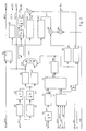
- a stereo multiplex signal MPX is supplied, which has a sampling rate of 228 kHz, which has proven to be advantageous in the previous digital signal processing. Since a substantially lower sampling rate is sufficient to form the first auxiliary signal SKU, the stereo multiplex signal MPX is passed via a low-pass filter 2 to a circuit 3 for reducing the sampling rate around the divider 24.
- the resulting signal is fed to a further low-pass filter 4, the cut-off frequency of which is very low, so that at its output there is practically only the DC voltage component of which the amount is formed at 5.
- This is compared in a comparator 6 with a constant C1 supplied at 7 of, for example, 0.07 (based on the maximum amplitude). If the amount of the DC voltage component is smaller than the constant C1, a 1 appears at the output x ⁇ y of the comparator 6, which is fed to an input of an AND circuit 8.
- a signal FST is fed to a further input 9 of the circuit arrangement according to FIG. 1, which corresponds to the field strength of the respectively received signal.
- This signal is low-pass filtered at 10 and compared to a constant C2 at 11. If the field strength is greater than a value specified by the constant C2, a 1 appears at the output x ⁇ y of the comparator 11, which also corresponds to the AND circuit 8 is directed. If both conditions are met, the stop signal SLS at the output 12 of the AND circuit 8 also assumes level 1.
- auxiliary signal SKU To derive the auxiliary signal SKU, a further comparator 13 is supplied, to which a constant C3 is supplied as a reference value. If the DC voltage component supplied by the magnitude generator 5 is greater than or equal to C3, the first auxiliary signal SKU assumes level 1 at the output 14.
- Fig. 2 shows the processing of a multiplex signal MPX1 up to audio signals for four channels.
- a digital stereo multiplex signal MPX1 is fed to an input 43 from an FM demodulator, while a further input 44 receives the signal AM1 from an AM demodulator.
- the sampling rate of the MPX1 signal is 456 kHz, which is an integer multiple of the carrier frequency of the radio data signal (57 kHz).
- this high sampling frequency requires a large number of arithmetic operations per second.
- the aim is therefore to work with the lowest possible sampling rates which are adapted to the bandwidth of the respective signal.
- the signal MPX1 is therefore subjected to a sampling rate halving at 45, for which purpose a low-pass filtering 46 is required beforehand.
- a low-pass filter 46 since the low-pass filter required per se, with a rectilinear frequency response over most of the pass band and a steep drop in the half-sampling frequency range, is very expensive, a low-pass filter 46 has been used which has a gradual drop.
- a compensation filter 47 with an opposite frequency response cancels the error that arises as a result.
- the signal MPX2 with a sampling frequency of 228 kHz is fed to a circuit 48 for automatic interference suppression. Such circuits suppress short pulse-shaped interference and have become known under the abbreviation ASU.
- the output signal MPX3 of the circuit 48 goes into a stereo decoder 49, which generates the two audio signals L1 and R1 (left and right), which are subjected to a sampling rate conversion around the divider 5 at 50.
- the resulting audio signals L2, R2 are fed via a circuit 51 with controllable damping as signals LFM and RFM inputs to a source switch 52. In a manner not shown, other audio signals can be fed to the source switch, for example from a CD player or a tape device.
- the output signals of the source switch 52 arrive as signals L, R at an audio processor 53, with the aid of which settings, such as volume, fader, balance and raising and lowering or raising, are carried out.
- the audio processor 53 has four outputs 54, 55, 56, 57, of which the signals LF, LR, RF and RR can each be fed to an output stage (not shown) for four loudspeakers.
- the stereo multiplex signal MPX2 also reaches a decoder 58 for traffic radio signals and / or radio data signals.
- the signal MPX2 is also required by a circuit 59 for the search stop and the first auxiliary signal SKU. An embodiment of this circuit has been described in connection with FIG. 1.
- a control unit 60 receives signals from the circuits 58, 59 and 42 and from the stereo decoder 49. It outputs signals to the circuit 42, the source switch 52 and the audio processor 53. Further connections of the control unit 60 - For example, with control and display devices - are not shown in Fig. 2.
- a signal is required which consists of the parts of the stereo multiplex signal above 60 kHz. This is generated in the circuit 41, to which the signals MPX1 and MPX2 are supplied.
- An exemplary embodiment of the circuit 41 is explained in more detail in patent application P 43 09 518.6 together with other details of the block diagrams according to FIGS. 2 and 3.
- FIG 3 illustrates details of circuit 42 ( Figure 2) used to derive signals describing the quality of the signals received.
- the output signal AM1 of an amplitude demodulator not shown, is supplied. It serves as a measure of the field strength.
- the signal AM1 with a sampling frequency of 456 kHz is first subjected to low-pass filtering in a filter 62. Together with the comb filter 65, this prevents that in the subsequent subsampling by a factor of 2 at 63 and later by a factor of 24 at 64, higher-frequency spectral components map to the direct component and falsify it in an impermissible manner.
- Another low-pass filtering (comb filter) 65 is provided between the scanning elements 63 and 64.
- the field strength signal thus decimated with respect to the sampling rates is averaged in two low-pass elements 66, 67 with different time constants.
- a switch 68 forwards one of the output signals of the low-pass elements 66, 67 as the signal AMC. This is weighted at 69 in the form of a noise curve to generate the noise attenuation A FE .
- the field strength signal of the smaller time constant, ie the "fast" field strength signal FST16 at the output of the Low-pass element 66 also serves to reduce the stereo channel separation D when the field strength drops.
- the further processing of the signals A FE and FST16 is explained in the patent application P 43 09 518.6 by the applicant.
- a high-pass detector 70, a symmetry detector 71 and a logic network 72 are used to generate the further signal DD2, the output signal DD1 of which is passed via a pulse width discriminator 73.
- the high-pass detector 70 which is explained in detail in FIG. 4, is supplied with an MPX5 signal via an input 74 and a sampling rate reduction 75, which contains portions of the stereo multiplex signal above 60 kHz, but which is already in the baseband are transformed.
- the second auxiliary signal BHD is set to level 1 in the high-pass detector 70 if spectral components above 60 kHz are present.
- This second auxiliary signal BHD together with the first auxiliary signal SKU supplied at 95, is fed to a non-AND circuit 96, which forms the adjacent channel interference signal DD3, which assumes the level, 0 in the event of adjacent channel interference.
- This signal is fed to an input of an integrator 81.
- Another output signal AHD of the high-pass detector 70 assumes the value 1 if the amplitude of signal components above 60 kHz is above a threshold value. This has the fundamental advantage of being able to react very punctually to any type of malfunction - including those that are not multi-way malfunctions. In extreme cases, however, it can lead to a fault being reported, but which does not yet lead to any audible disturbances in the receiver's external NF signal. In this case, however, the measures envisaged for masking faults would still occur be initiated.
- the symmetry of the carrier-frequency stereo difference signal is evaluated to detect audible interference that is not an adjacent channel interference. It is important in this procedure, on the one hand, that an undisturbed signal must be symmetrical to the carrier due to the two-sideband amplitude modulation, and, on the other hand, that the useful signal is considered directly here. An asymmetry therefore leads to the conclusion that there is an interference that can also be heard in the LF signal.
- Signals are fed to the symmetry detector 71 via inputs 76 to 79 from a stereo decoder (FIG. 2), which essentially represent the product of the carrier-frequency stereo difference signal with a reference carrier which is in quadrature with the subcarrier.
- the output signal ASD of the symmetry detector assumes the value 1 if there is asymmetry.
- the use of one of the signals AHD or ASD as a further signal DD2 already brings considerable advantages.
- both detectors 70, 71 are provided, the output signals AHD and ASD being routed via a logic network 72.
- this has the advantage that in the case of pure mono broadcasts in which no carrier-frequency stereo difference signal is transmitted, the further auxiliary signal DD2 is derived by the high-pass detector 70.
- the derivation of the further signal DD2 is also possible with methods for stereo signal transmission which deviate from the European standard - for example with the FMX method in the USA.
- the logical network enables the selection or the type of logical combination of the two signals AHD and ASD to signal DD1.
- the signal DD1 is over a Pulse width discriminator 73 passed, which ensures that the output signal DD2 only indicates a fault when the input signal DD1 is active for an adjustable minimum period.
- the signal DD2 switches between a large and a small time constant when the field strength signal is formed.
- the signal DD2 also serves as a trigger signal for two asymmetrical integrators 80, 81, of which an exemplary embodiment is shown in FIG. 5.
- the output signals AT1 and AMU of the asymmetrical integrators 80, 81 jump to 0 at the moment of triggering or to a preset value between 0 and 1 and remain at these values as long as DD2 and DD3 are at zero, in order to then linearly increase with adjustable time constants to increase a maximum value.
- the signal AT1 is fed to a multiplier 83 together with the field strength signal WF2 weighted at 82. This forms a signal that masks interference in the LF signal by reducing the stereo channel separation. This is multiplied in a further multiplier 84 by a signal FMO supplied at 85, which is used to forcibly cancel the stereo channel separation.
- Signal D can be taken from output 86 and fed to the stereo decoder.
- the output signal AMU of the asymmetrical integrator 81 is fed together with the signal A FE to a further multiplier 87, which, after limitation at 97 and sampling rate conversion at 98 and 99, produces a signal AFE_AMU which attenuates the LF signal by a maximum of that caused by the limiter 97 causes predetermined value that can be taken from the output 88.
- the circuit arrangement according to FIG. 3 has three further outputs 89, 90, 91, at which signals can be removed which describe the field strength.
- the FST16 signal is 16 bit accurate. For some purposes, however, a signal with lower accuracy is also sufficient, which is why a field strength signal FST8 with a bit width of 8 is generated with the aid of a compression characteristic curve 92.
- the signals FST16 and FST8 are fast enough for the purpose of identifying the signal quality, but they are not free from a certain inertia due to the filters described in connection with FIG. 3 and possibly due to the amplitude demodulation.
- a signal VFST can be fed in via an input 93 from a microcontroller (not shown).
- a signal DFST is generated from this signal and the signal FST16 with the aid of a comparator 94, the respective level (0 or 1) of which depends on whether the signal VFST or the signal FST16 is larger.
- the signal DFST which can be taken off at output 89 indicates the direction of change of the field strength.
- the high-pass detector 70 is explained in more detail below with reference to FIG. 4.
- the signal MPX5 can be fed to an input 100 of the high-pass detector in accordance with FIG. If the averaged signal exceeds a threshold HDS, the output signal of a comparator consisting of a subtractor 103 and a sign recognition 104, 105 assumes the value 1.
- the signal AHD at the output 106 also assumes the value 1 if the sign of the output signal of the subtractor 103 is positive.
- Another comparator is formed by a further subtractor 107 and a further sign recognition 108, 109.
- the second auxiliary signal BHD at output 110 assumes the value 1 if the higher-frequency spectral components exceed the reference value HDT.
- FIG. 5 An embodiment of the asymmetrical integrator 81 (FIG. 3) is shown in FIG. 5.
- Two integrators are provided per se, to which the signals DD2 and DD3 can be fed via inputs 111 and 112.
- Each integrator consists of an adder 113, 114, two format converters 115, 116 and 119, 120, a multiplier 117, 118 and a delay 121, 122 by one sampling period.
- AST2 and AST5 are applied.
- the signal DD3 changes to the value 0. This has the consequence that the integrator for the adjacent channel interference signal DD3 is set to 0.
- DD3 At the end of an adjacent channel disturbance, DD3 returns to level 1, whereupon the integrator starts up to the value 1 by integrating the constants AST5.
- the procedure for signal DD2 is similar.
- the output signals of both integrators are evaluated at 125, 126 with a constant AST3, AST6 and then added at 127, 128 to a further constant AST4, AST7.
- the results are multiplied together at 129 and can be taken from an output 130 as signal A MU .
Landscapes
- Engineering & Computer Science (AREA)
- Computer Networks & Wireless Communication (AREA)
- Signal Processing (AREA)
- Noise Elimination (AREA)
- Stereo-Broadcasting Methods (AREA)
- Monitoring And Testing Of Transmission In General (AREA)
- Time-Division Multiplex Systems (AREA)
- Stereophonic System (AREA)
Abstract
Description
Die Erfindung betrifft eine Schaltungsanordnung zur Erkennung von Nachbarkanalstörungen in einem Stereo-Rundfunkempfänger, bei dem ein Stereo-Multiplexsignal vorhanden ist. Ferner beschäftigt sich die Erfindung mit Maßnahmen zur Reduzierung der subjektiv empfundenen Störwirkung von Nachbarkanalstörungen.The invention relates to a circuit arrangement for the detection of adjacent channel interference in a stereo broadcast receiver in which a stereo multiplex signal is present. Furthermore, the invention is concerned with measures for reducing the subjectively perceived interference effect of adjacent channel interference.
Signale aus Nachbarkanälen können beim UKW-Empfang aufgrund einer unzureichenden Filterung in den HF-Vorstufen und in der Zwischenfrequenzebene zu Störungen im jeweils empfangenen Kanal führen. Die Aufgabe der vorliegenden Erfindung besteht daher darin, solche Störungen zu erkennen, wobei dieses vorzugsweise mit digitalen Schaltungen, vorzugsweise in integrierter Schaltungstechnik, verwirklicht werden soll. Es soll ferner im Rahmen der Erfindung eine Reduzierung der subjektiven Störwirkung von Nachbarkanalstörungen erzielt werden.Signals from neighboring channels can lead to interference in the received channel due to insufficient filtering in the RF pre-stages and in the intermediate frequency level. The object of the present invention is therefore to detect such faults, which should preferably be implemented using digital circuits, preferably using integrated circuit technology. It is also intended within the scope of the invention to reduce the subjective interference effect of adjacent channel interference.
Die Erkennung von Nachbarkanalstörungen wird bei der erfindungsgemäßen Schaltungsanordnung dadurch bewirkt, daß in Abhängigkeit von einem Gleichspannungsanteil und in Abhängigkeit von Spektralkomponenten oberhalb von 60 kHz ein die Nachbarkanalstörungen anzeigendes Signal (Nachbarkanalstörungssignal) abgeleitet wird.The detection of adjacent channel interference is effected in the circuit arrangement according to the invention in that, depending on a DC voltage component and in Depending on spectral components above 60 kHz, a signal indicating the adjacent channel interference (adjacent channel interference signal) is derived.
Durch die Verwendung von zwei Kriterien zum Erkennen von Nachbarkanalstörungen ist bei der erfindungsgemäßen Schaltungsanordnung eine Unterscheidung zwischen Nachbarkanalstörungen und andersartigen Störungen, die ebenfalls zu höherfrequenten Spektralkomponenten im Stereo-Multiplexsignal führen, möglich. Derartige Störungen sind beispielsweise Mehrwegeempfang oder Zündstörungen.By using two criteria for recognizing adjacent channel interference, a distinction can be made between adjacent channel interference and other types of interference in the circuit arrangement according to the invention, which also lead to higher-frequency spectral components in the stereo multiplex signal. Such interference is, for example, multi-path reception or ignition interference.
Obwohl im Rahmen der Erfindung als Nachbarkanalstörung auch andere Signale abgeleitet werden können, ist die Ableitung eines binären Signals, das lediglich das Vorhandensein oder das Nichtvorhandensein von Nachbarkanalstörungen kennzeichnet, für eine Weiterverarbeitung in vielen Fällen besonders vorteilhaft.Although other signals can also be derived as an adjacent channel interference in the context of the invention, the derivation of a binary signal which merely indicates the presence or absence of adjacent channel interference is particularly advantageous in many cases for further processing.
Bei einer Weiterbildung der erfindungsgemäßen Schaltungsanordnung ist daher vorgesehen, daß ein erstes Hilfssignal abgeleitet wird, wenn der Gleichspannungsanteil des Stereo-Multiplexsignals größer als ein erster Bezugswert ist, daß ein zweites Hilfssignal gebildet wird, wenn die Amplituden der Spektralkomponenten oberhalb von 60 kHz des Stereo-Multiplexsignals größer als ein zweiter Bezugswert sind, und daß das erste und das zweite Hilfssignal zur Bildung des Nachbarkanalstörungssignals und-verknüpft werden.In a further development of the circuit arrangement according to the invention, it is therefore provided that a first auxiliary signal is derived when the direct voltage component of the stereo multiplex signal is greater than a first reference value, that a second auxiliary signal is formed when the amplitudes of the spectral components above 60 kHz of the stereo Multiplex signals are greater than a second reference value, and that the first and the second auxiliary signal and are combined to form the adjacent channel interference signal.
Vorteilhafte Ausgestaltungen der erfindungsgemäßen Schaltungsanordnung bestehen darin, daß das erste Hilfssignal dadurch abgeleitet wird, daß das Stereo-Multiplexsignal tiefpaßgefiltert und gleichgerichtet wird und daß das gleichgerichtete Signal mit dem ersten Bezugswert verglichen wird und daß das hochpaßgefilterte Stereo-Multiplexsignal gleichgerichtet und tiefpaßgefiltert wird und daß das tiefpaßgefilterte Signal mit dem zweiten Bezugswert verglichen wird.Advantageous embodiments of the circuit arrangement according to the invention consist in that the first auxiliary signal is derived in that the stereo multiplex signal is low-pass filtered and rectified and in that the rectified signal is compared with the first reference value and that the high-pass filtered Stereo multiplex signal is rectified and low-pass filtered and that the low-pass filtered signal is compared with the second reference value.
Eine Verminderung der subjektiv empfundenen Störwirkung mit Hilfe des Nachbarkanalstörungssignals kann durch eine Dämpfung der Audiosignale um beispielsweise 10dB bis 20dB bestehen. Eine besonders vorteilhafte Möglichkeit zur Reduzierung der Störwirkung besteht jedoch darin, daß das Nachbarkanalstörungssignal einem Integrator zuführbar ist, der in einer Richtung bei vorhandenen Nachbarkanalstörungen und in entgegengesetzter Richtung bei nichtvorhandenen Nachbarkanalstörungen integriert, und daß das Ausgangssignal des Integrators eine Dämpfung von aus dem Stereo-Multiplexsignal gewonnenen Audiosignalen derart bewirkt, daß bei Integration in entgegengesetzter Richtung die Dämpfung zunimmt.A reduction in the subjectively perceived interference effect with the aid of the adjacent channel interference signal can result from an attenuation of the audio signals by, for example, 10 dB to 20 dB. A particularly advantageous way of reducing the interference effect is, however, that the adjacent channel interference signal can be fed to an integrator which integrates in one direction in the presence of adjacent channel interference and in the opposite direction in the absence of adjacent channel interference, and in that the output signal of the integrator attenuates from the stereo multiplex signal obtained audio signals in such a way that when integrated in the opposite direction, the attenuation increases.
Bei dieser Weiterbildung wird in vorteilhafter Weise die Dauer von Nachbarkanalstörungen berücksichtigt. Dabei ist vorteilhaft, wenn die Zeitkonstante des Integrators in der einen Richtung kleiner als in der entgegengesetzten Richtung oder gleich Null ist. Um eine zu starke Dämpfung zu vermeiden, kann dabei vorgesehen sein, daß das Ausgangssignal des Integrators über einen Begrenzer geleitet wird.In this development, the duration of adjacent channel interference is taken into account in an advantageous manner. It is advantageous if the time constant of the integrator in one direction is less than in the opposite direction or equal to zero. In order to avoid excessive damping, it can be provided that the output signal of the integrator is passed through a limiter.
Eine andere Weiterbildung der erfindungsgemäßen Schaltungsanordnung besteht darin, daß bei Ableitung weiterer die Empfangsqualität darstellender Signale das Nachbarkanalstörungssignal diesen Signalen überlagert wird und daß das dadurch entstehende Signal anschließend begrenzt wird.Another further development of the circuit arrangement according to the invention consists in that when further signals representing the reception quality are derived, the adjacent channel interference signal is superimposed on these signals and that the signal which is produced as a result is subsequently limited.
Ein Ausführungsbeispiel der Erfindung ist in der Zeichnung anhand mehrerer Figuren dargestellt und in der nachfolgenden Beschreibung näher erläutert. Es zeigt:
- Fig. 1
- ein Blockschaltbild zur Ableitung des ersten Hilfssignals bei der erfindungsgemäßen Schaltungsanordnung,
- Fig. 2
- ein Blockschaltbild eines hochintegrierten Stereo-Rundfunkempfängers mit der erfindungsgemäßen Schaltungsanordnung,
- Fig. 3
- ein Teil des Blockschaltbildes nach Fig. 2 in detaillierterer Ausführung,
- Fig. 4
- ein Blockschaltbild einer Schaltungsanordnung zur Ableitung des zweiten Hilfssignals und
- Fig. 5
- ein Blockschaltbild einer Schaltungsanordnung zur Bildung eines Steuersignals für die Dämpfung der Audiosignale aus dem Nachbarkanalstörungssignal und einem weiteren Signal.
- Fig. 1
- 2 shows a block diagram for deriving the first auxiliary signal in the circuit arrangement according to the invention,
- Fig. 2
- 2 shows a block diagram of a highly integrated stereo radio receiver with the circuit arrangement according to the invention,
- Fig. 3
- 2 a part of the block diagram according to FIG.
- Fig. 4
- a block diagram of a circuit arrangement for deriving the second auxiliary signal and
- Fig. 5
- a block diagram of a circuit arrangement for forming a control signal for the attenuation of the audio signals from the adjacent channel interference signal and another signal.
Gleiche Teile sind in den Figuren mit gleichen Bezugszeichen versehen. Die erfindungsgemäße Schaltungsanordnung kann auf verschiedene Weise verwirklicht werden. So können beispielsweise einzelne oder Gruppen der dargestellten Blöcke durch geeignete Schaltungen, insbesondere integrierte Schaltungen, realisiert werden. Bei sehr hohem Integrationsgrad ist es ferner möglich, die gesamte digitale Signalverarbeitung des Empfängers in einem integrierten Schaltkreis zu realisieren, wobei Signalverarbeitungsschritte, wie beispielsweise Filterungen oder nichtlineare Wichtungen, durch Rechenoperationen durchgeführt werden. Innerhalb eines integrierten Schaltkreises können zur Realisierung eines Empfängers mit der erfindungsgemäßen Schaltungsanordnung auch digitale Signalprozessoren und andere digitale Schaltungen, wie beispielsweise Schieberegister, Flip-Flops usw., gemeinsam angeordnet sein.Identical parts are provided with the same reference symbols in the figures. The circuit arrangement according to the invention can be implemented in various ways. For example, individual or groups of the blocks shown can be implemented using suitable circuits, in particular integrated circuits. With a very high degree of integration, it is also possible to implement the entire digital signal processing of the receiver in an integrated circuit, signal processing steps, such as filtering or nonlinear weighting, being carried out by arithmetic operations. An integrated circuit can be used to implement a receiver In the circuit arrangement according to the invention, digital signal processors and other digital circuits, such as shift registers, flip-flops etc., can be arranged together.
Die Schaltungsanordnung nach Fig. 1 dient außer zur Ableitung eines Stopp-Signals für den Sender-Suchlauf, was in der Patentanmeldung P 43 11 933.6 der Anmelderin beschrieben ist, zur Ableitung des ersten Hilfssignals SKU. Bei 1 wird ein Stereo-Multiplexsignal MPX zugeführt, das eine Abtastrate von 228 kHz aufweist, welche sich als vorteilhaft bei der vorangegangenen digitalen Signalverarbeitung herausgestellt hat. Da zur Bildung des ersten Hilfssignals SKU eine wesentlich niedrigere Abtastrate genügt, wird das Stereo-Multiplexsignal MPX über einen Tiefpaß 2 zu einer Schaltung 3 zur Abtastratenreduzierung um den Teiler 24 geleitet.1 serves to derive a stop signal for the station search, which is described in the
Das resultierende Signal wird einem weiteren Tiefpaß 4 zugeführt, dessen Grenzfrequenz sehr niedrig ist, so daß sich an seinem Ausgang praktisch nur der Gleichspannungsanteil ergibt, von welchem bei 5 der Betrag gebildet wird. Dieser wird in einem Komparator 6 mit einer bei 7 zugeführten Konstanten C1 von beispielsweise 0,07 (bezogen auf die Maximalamplitude) verglichen. Ist der Betrag des Gleichspannungsanteils kleiner als die Konstante C1, erscheint am Ausgang x≧y des Komparators 6 eine 1, die einem Eingang einer Und-Schaltung 8 zugeleitet wird.The resulting signal is fed to a further low-
Einem weiteren Eingang 9 der Schaltungsanordnung nach Fig. 1 wird ein Signal FST zugeleitet, welches der Feldstärke des jeweils empfangenen Signals entspricht. Dieses Signal wird bei 10 tiefpaßgefiltert und bei 11 mit einer Konstanten C2 verglichen. Ist die Feldstärke größer als ein durch die Konstante C2 vorgegebener Wert, so erscheint am Ausgang x≧y des Komparators 11 eine 1, die ebenfalls zur Und-Schaltung 8 geleitet wird. Sind beide Bedingungen erfüllt, so nimmt das Stopp-Signal SLS am Ausgang 12 der Und-Schaltung 8 ebenfalls den Pegel 1 an.A signal FST is fed to a
Zur Ableitung des Hilfssignals SKU ist ein weiterer Komparator 13 zugeführt, dem als Bezugswert eine Konstante C3 zugeführt wird. Ist der von dem Betragsbildner 5 zugeführte Gleichspannungsanteil größer oder gleich C3, nimmt das erste Hilfssignal SKU am Ausgang 14 den Pegel 1 an.To derive the auxiliary signal SKU, a
Fig. 2 zeigt die Verarbeitung eines Multiplexsignals MPX1 bishin zu Audiosignalen für vier Kanäle. Einem Eingang 43 wird von einem FM-Demodulator ein digitales Stereo-Multiplex-Signal MPX1 zugeleitet, während ein weiterer Eingang 44 von einem AM-Demodulator das Signal AM1 erhält. Bei einem praktisch ausgeführten Ausführungsbeispiel beträgt die Abtastrate des Signals MPX1 456 kHz, was ein ganzzahliges Vielfaches der Trägerfrequenz des Radio-Daten-Signals (57 kHz) ist.Fig. 2 shows the processing of a multiplex signal MPX1 up to audio signals for four channels. A digital stereo multiplex signal MPX1 is fed to an
Diese hohe Abtastfrequenz erfordert jedoch eine große Anzahl von Rechenoperationen je Sekunde. Bei dem dargestellten Rundfunkempfänger ist man deshalb bestrebt, mit möglichst geringen Abtastraten zu arbeiten, die an die Bandbreite des jeweiligen Signals angepaßt sind. Deshalb wird das Signal MPX1 bei 45 einer Abtastratenhalbierung unterzogen, wozu zuvor eine Tiefpaßfilterung 46 erforderlich ist. Da jedoch das an sich erforderliche Tiefpaßfilter mit einem geradlinigen Frequenzgang über den größten Teil des Durchlaßbereiches und einem steilen Abfall im Bereich der halben Abtastfrequenz sehr aufwendig ist, wurde ein Tiefpaßfilter 46 verwendet, das einen allmählichen Abfall aufweist. Ein Kompensationsfilter 47 mit einem entgegengesetzten Frequenzgang hebt jedoch den dadurch entstehenden Fehler wieder auf.However, this high sampling frequency requires a large number of arithmetic operations per second. In the radio receiver shown, the aim is therefore to work with the lowest possible sampling rates which are adapted to the bandwidth of the respective signal. The signal MPX1 is therefore subjected to a sampling rate halving at 45, for which purpose a low-
Das Signal MPX2 mit einer Abtastfrequenz von 228 kHz wird einer Schaltung 48 zur automatischen Störunterdrückung zugeleitet. Derartige Schaltungen unterdrücken kurze impulsförmige Störungen und sind unter dem Kürzel ASU bekanntgeworden. Das Ausgangssignal MPX3 der Schaltung 48 gelangt in einen Stereo-Decoder 49, der die beiden Audiosignale L1 und R1 (links und rechts) erzeugt, die bei 50 einer Abtastratenwandlung um den Teiler 5 unterzogen werden. Die dadurch entstehenden Audiosignale L2, R2 werden über eine Schaltung 51 mit steuerbarer Dämpfung als Signale LFM und RFM Eingängen eines Quellenumschalters 52 zugeführt. In nicht dargestellter Weise können dem Quellenumschalter andere Audiosignaie zugeleitet werden, beispielsweise von einem CD-Spieler oder einem Bandgerät.The signal MPX2 with a sampling frequency of 228 kHz is fed to a
Die Ausgangssignale des Quellenumschalters 52 gelangen als Signale L, R zu einem Audioprozessor 53, mit dessen Hilfe Einstellungen, wie beispielsweise Lautstärke, Fader, Balance und Höhen- und Tiefenabsenkung bzw. -anhebung, vorgenommen werden. Der Audioprozessor 53 hat vier Ausgänge 54, 55, 56, 57, von denen die Signale LF, LR, RF und RR jeweils einer nicht dargestellten Endstufe für vier Lautsprecher zugeführt werden können.The output signals of the
Das Stereo-Multiplex-Signal MPX2 gelangt ferner zu einem Decoder 58 für Verkehrsfunksignale und/oder Radio-Daten-Signale. Außerdem wird das Signal MPX2 von einer Schaltung 59 für den Suchlaufstopp und das erste Hilfssignal SKU benötigt. Ein Ausführungsbeispiel dieser Schaltung wurde im Zusammenhang mit Fig. 1 beschrieben.The stereo multiplex signal MPX2 also reaches a
Eine Steuereinheit 60 erhält Signale von den Schaltungen 58, 59 und 42 sowie vom Stereo-Decoder 49. Sie gibt Signale ab an die Schaltung 42, den Quellenumschalter 52 und den Audioprozessor 53. Weitere Verbindungen der Steuereinheit 60 - beispielsweise mit Bedien- und Anzeigevorrichtungen - sind in Fig. 2 nicht dargestellt.A
Für die Ableitung des zweiten Hilfssignals wird ein Signal benötigt, das aus den Anteilen des Stereo-Multiplex-Signals oberhalb von 60 kHz besteht. Dieses wird in der Schaltung 41 erzeugt, welcher die Signale MPX1 und MPX2 zugeführt werden. Ein Ausführungsbeispiel der Schaltung 41 ist in der Patentanmeldung P 43 09 518.6 zusammen mit anderen Details der Blockschaltbilder nach den Figuren 2 und 3 näher erläutert.For the derivation of the second auxiliary signal, a signal is required which consists of the parts of the stereo multiplex signal above 60 kHz. This is generated in the
Fig. 3 stellt Details der Schaltung 42 (Fig. 2) dar, die zur Ableitung von Signalen dient, welche die Qualität der empfangenen Signale beschreiben. Bei 61 wird das Ausgangssignal AM1 eines nicht dargestellten Amplitudendemodulators zugeführt. Es dient als Maß für die Feldstärke. Das Signal AM1 mit einer Abtastfrequenz von 456 kHz wird zunächst in einem Filter 62 einer Tiefpaßfilterung unterzogen. Dieses verhindert zusammen mit dem Kammfilter 65, daß sich bei der nachfolgenden Unterabtastung um den Faktor 2 bei 63 und später um den Faktor 24 bei 64 höherfrequente Spektralkomponenten auf den Gleichanteil abbilden und diesen in unzulässiger Weise verfälschen. Eine weitere Tiefpaßfilterung (Kammfilter) 65 ist zwischen den Abtastgliedern 63 und 64 vorgesehen.Figure 3 illustrates details of circuit 42 (Figure 2) used to derive signals describing the quality of the signals received. At 61, the output signal AM1 of an amplitude demodulator, not shown, is supplied. It serves as a measure of the field strength. The signal AM1 with a sampling frequency of 456 kHz is first subjected to low-pass filtering in a
Das somit bezüglich der Abtastraten dezimierte Feldstärkesignal erfährt in zwei Tiefpaßgliedern 66, 67 eine Mittelung mit unterschiedlichen Zeitkonstanten. Ein Umschalter 68 leitet in Abhängigkeit eines Signals DD2 eines der Ausgangssignale der Tiefpaßglieder 66, 67 als Signal AMC weiter. Dieses wird bei 69 in Form einer Aufrauschkurve zur Erzeugung der Aufrauschdämpfung AFE gewichtet. Das Feldstärkesignal der kleineren Zeitkonstante, also das "schnelle" Feldstärkesignal FST16 am Ausgang des Tiefpaßgliedes 66 dient außerdem zur Reduzierung der Stereokanaltrennung D bei Absinken der Feldstärke. Die weitere Verarbeitung der Signale AFE und FST16 ist in der Patentanmeldung P 43 09 518.6 der Anmelderin erläutert.The field strength signal thus decimated with respect to the sampling rates is averaged in two low-
Zur Erzeugung des weiteren Signals DD2 dienen ein Hochpaß-Detektor 70, ein Symmetrie-Detektor 71 und ein logisches Netzwerk 72, dessen Ausgangssignal DD1 über einen Impulsbreitendiskriminator 73 geleitet wird. Dem Hochpaß-Detektor 70, der im einzelnen in Fig. 4 erläutert wird, wird über einen Eingang 74 und eine Abtastratenreduzierung 75 ein Signal MPX5 zugeführt, das Anteile des Stereo-Multiplex-Signals oberhalb von 60 kHz enthält, die jedoch bereits in das Basisband transformiert sind.A high-
In dem Hochpaß-Detektor 70 wird unter anderem das zweite Hilfssignal BHD auf den Pegel 1 gesetzt, wenn Spektralkomponenten oberhalb von 60 kHz vorhanden sind. Dieses zweite Hilfssignal BHD wird zusammen mit dem bei 95 zugeführten ersten Hilfssignal SKU einer Nicht-Und-Schaltung 96 zugeführt, wodurch das Nachbarkanalstörungssignal DD3 gebildet wird, das im Falle von Nachbarkanalstörungen den Pegel, 0 annimmt. Dieses Signal wird einem Eingang eines Integrators 81 zugeführt.Among other things, the second auxiliary signal BHD is set to
Ein weiteres Ausgangssignal AHD des Hochpaß-Detektors 70 nimmt den Wert 1 an, wenn die Amplitude von Signalanteilen oberhalb von 60 kHz oberhalb eines Schwellwertes liegen. Dieses hat den grundsätzlichen Vorteil, sehr pünktlich auf jede Art von Störungen - also auch auf solche, die keine Mehrwegestörungen sind - zu reagieren. Es kann jedoch im Extremfall dazu führen, daß zwar eine Störung gemeldet wird, die jedoch im ausseitigen NF-Signal des Empfängers noch zu keinen hörbaren Störungen führt. Trotzdem würden in diesem Fall die zur Maskierung von Störungen vorgesehenen Maßnahmen eingeleitet werden.Another output signal AHD of the high-
Zur Erkennung von hörbaren Störungen, die keine Nachbarkanalstörungen sind, erfolgt eine Auswertung der Symmetrie des trägerfrequenten Stereo-Differenzsignals. Wesentlich ist bei diesem Vorgehen einerseits, daß ein ungestörtes Signal aufgrund der Zwei-Seitenband-Amplitudenmodulation symmetrisch zum Träger sein muß, und andererseits, daß hier unmittelbar das Nutzsignal betrachtet wird. Eine Asymmetrie läßt daher den Schluß zu, daß eine auch im NF-Signal hörbare Störung vorliegt. Über Eingänge 76 bis 79 werden dem Symmetrie-Detektor 71 von einem Stereo-Decoder (Fig. 2) Signale zugeführt, die im wesentlichen das Produkt des trägerfrequenten Stereo-Differenzsignals mit einem Referenzträger darstellen, der in Quadratur zum Hilfsträger steht. Das Ausgangssignal ASD des Symmetrie-Detektors nimmt den Wert 1 an, wenn eine Asymmetrie vorhanden ist.The symmetry of the carrier-frequency stereo difference signal is evaluated to detect audible interference that is not an adjacent channel interference. It is important in this procedure, on the one hand, that an undisturbed signal must be symmetrical to the carrier due to the two-sideband amplitude modulation, and, on the other hand, that the useful signal is considered directly here. An asymmetry therefore leads to the conclusion that there is an interference that can also be heard in the LF signal. Signals are fed to the
Bei vielen Anwendungsfällen bringt die Verwendung eines der Signale AHD bzw. ASD als weiteres Signal DD2 bereits erhebliche Vorteile. Bei dem dargestellten Ausführungsbeispiel sind jedoch beide Detektoren 70, 71 vorgesehen, wobei die Ausgangssignale AHD und ASD über ein logisches Netzwerk 72 geleitet werden. Dieses hat einerseits den Vorteil, daß bei reinen Mono-Sendungen, bei denen kein trägerfrequentes Stereo-Differenzsignal gesendet wird, die Ableitung des weiteren Hilfssignals DD2 durch den Hochpaß-Detektor 70 erfolgt. Ebenso ist die Ableitung des weiteren Signals DD2 auch bei von der europäischen Norm abweichenden Verfahren zur Stereo-Signalübertragung möglich - beispielsweise bei dem FMX-Verfahren in den USA.In many applications, the use of one of the signals AHD or ASD as a further signal DD2 already brings considerable advantages. In the exemplary embodiment shown, however, both
Das logische Netzwerk ermöglicht die Auswahl oder die Art der logischen Verknüpfung der beiden Signale AHD und ASD zum Signal DD1. Das Signal DD1 wird über einen Impulsbreitendiskriminator 73 geleitet, der dafür sorgt, daß das Ausgangssignal DD2 erst dann eine Störung anzeigt, wenn das Eingangssignal DD1 für eine einstellbare Mindestzeitdauer aktiv ist. Wie bereits erwähnt, schaltet das Signal DD2 zwischen einer großen und einer kleinen Zeitkonstanten bei der Bildung des Feldstärkesignals um. Ferner dient das Signal DD2 als Triggersignal für zwei asymmetrische Integratoren 80, 81, von denen ein Ausführungsbeispiel in Fig. 5 dargestellt ist.The logical network enables the selection or the type of logical combination of the two signals AHD and ASD to signal DD1. The signal DD1 is over a
Die Ausgangssignale AT1 und AMU der asymmetrischen Integratoren 80, 81 springen im Moment des Triggerns auf 0 bzw. auf einen voreingestellten Wert zwischen 0 und 1 und bleiben solange auf diesen Werten, wie DD2 und DD3 auf Null liegen, um dann mit einstellbaren Zeitkonstanten linear auf einen Maximalwert anzusteigen. Das Signal AT1 wird gemeinsam mit dem bei 82 gewichteten Feldstärkesignal WF2 einem Multiplizierer 83 zugeführt. Dadurch wird ein Signal gebildet, das eine Maskierung von Störungen im NF-Signal durch eine Verminderung der Stereokanaltrennung bewirkt. Dieses wird in einem weiteren Multiplizierer 84 mit einem bei 85 zugeführten Signal FMO multipliziert, das zur zwangsweisen Aufhebung der Stereokanaltrennung dient. Vom Ausgang 86 kann das Signal D entnommen und dem Stereo-Decoder zugeführt werden.The output signals AT1 and AMU of the
Das Ausgangssignal AMU des asymmetrischen Integrators 81 wird zusammen mit dem Signal AFE einem weiteren Multiplizierer 87 zugeführt, wodurch nach Begrenzung bei 97 und Abtastratenwandlung bei 98 und 99 ein Signal AFE_AMU entsteht, das eine Dämpfung des NF-Signals um maximal den durch den Begrenzer 97 vorgegebenen Wert bewirkt, das dem Ausgang 88 entnehmbar ist.The output signal AMU of the
In einem digitalen Rundfunkempfänger werden an mehreren Stellen Informationen zur Feldstärke benötigt. Dazu weist die Schaltungsanordnung nach Fig. 3 drei weitere Ausgänge 89, 90, 91 auf, an denen Signale abnehmbar sind, welche die Feldstärke beschreiben. Das Signal FST16 ist 16 Bit genau. Für manche Zwecke genügt jedoch auch ein Signal mit geringerer Genauigkeit, deswegen wird mit Hilfe einer Kompressionskennlinie 92 ein Feldstärkesignal FST8 mit einer Bitbreite von 8 erzeugt.Information about the field strength is required in several places in a digital radio receiver. For this purpose, the circuit arrangement according to FIG. 3 has three
Die Signale FST16 und FST8 sind zwar für die Zwecke der Kennung der Signalqualität ausreichend schnell, sie sind jedoch durch die im Zusammenhang mit Fig. 3 beschriebenen Filter und gegebenenfalls durch die Amplituden-Demodulation nicht frei von einer gewissen Trägheit. Über einen Eingang 93 ist von einem nicht dargestellten Microcontroller ein Signal VFST zuführbar. Aus diesem Signal und dem Signal FST16 wird mit Hilfe eines Komparators 94 ein Signal DFST erzeugt, dessen jeweiliger Pegel (0 bzw. 1) davon abhängt, ob das Signal VFST oder das Signal FST16 größer ist. Dadurch zeigt das am Ausgang 89 abnehmbare Signal DFST die Änderungsrichtung der Feldstärke an.The signals FST16 and FST8 are fast enough for the purpose of identifying the signal quality, but they are not free from a certain inertia due to the filters described in connection with FIG. 3 and possibly due to the amplitude demodulation. A signal VFST can be fed in via an
Der Hochpaß-Detektor 70 wird im folgenden anhand von Fig. 4 näher erläutert. Einem Eingang 100 des Hochpaß-Detektors gemäß Fig. 4 ist das Signal MPX5 zuführbar, das nach einer Betragsbildung 101 mit Hilfe eines Tiefpaßfilters 102 gemittelt wird. Überschreitet das gemittelte Signal eine Schwelle HDS, nimmt das Ausgangssignal eines aus einem Subtrahierer 103 und einer Vorzeichenerkennung 104, 105 bestehenden Komparators den Wert 1 an. Das Signal AHD am Ausgang 106 nimmt ebenfalls den Wert 1 an, wenn das Vorzeichen des Ausgangssignals des Subtrahierers 103 positiv ist. Ein weiterer Komparator wird von einem weiteren Subtrahierer 107 und einer weiteren Vorzeichenerkennung 108, 109 gebildet. Das zweite Hilfssignal BHD am Ausgang 110 nimmt den Wert 1 an, wenn die höherfrequenten Spektralanteile den Bezugswert HDT überschreiten.The high-
Ein Ausführungsbeispiel für den asymmetrischen Integrator 81 (Fig. 3) ist in Fig. 5 dargestellt. Dabei sind an sich zwei Integratoren vorgesehen, denen über Eingänge 111 und 112 die Signale DD2 und DD3 zuführbar sind. Jeweils ein Integrator besteht aus einem Addierer 113, 114, zwei Formatwandlern 115, 116 und 119, 120, einem Multiplizierer 117, 118 sowie einer Verzögerung 121, 122 um eine Abtastperiode. Bei 123 und 124 werden Integrationskonstanten AST2 und AST5 zugeführt. Am Beginn einer Nachbarkanalstörung wechselt das Signal DD3 auf den Wert 0. Dieses hat zur Folge, daß der Integrator für das Nachbarkanalstörungssignal DD3 auf 0 gesetzt wird. Diesen Ausgangswert behält der Integrator solange bei, wie Nachbarkanalstörungen vorliegen, das heißt, solange DD3 = 0 gilt.An embodiment of the asymmetrical integrator 81 (FIG. 3) is shown in FIG. 5. Two integrators are provided per se, to which the signals DD2 and DD3 can be fed via
Am Ende einer Nachbarkanalstörung nimmt DD3 wieder den Pegel 1 an, worauf der Integrator durch die Integration der Konstanten AST5 bis auf den Wert 1 hochläuft. In ähnlicher Weise wird mit dem Signal DD2 verfahren. Die Ausgangssignale beider Integratoren werden bei 125, 126 mit je einer Konstanten AST3, AST6 bewertet und anschließend bei 127, 128 zu je einer weiteren Konstanten AST4, AST7 addiert. Die Ergebnisse werden bei 129 miteinander multipliziert und kann einem Ausgang 130 als Signal AMU entnommen werden.At the end of an adjacent channel disturbance, DD3 returns to
Claims (9)
Applications Claiming Priority (2)
| Application Number | Priority Date | Filing Date | Title |
|---|---|---|---|
| DE4338700 | 1993-11-12 | ||
| DE4338700A DE4338700C2 (en) | 1993-11-12 | 1993-11-12 | Circuit arrangement for the detection of adjacent channel interference in a stereo multiplex broadcast receiver |
Publications (3)
| Publication Number | Publication Date |
|---|---|
| EP0653850A2 true EP0653850A2 (en) | 1995-05-17 |
| EP0653850A3 EP0653850A3 (en) | 1995-11-29 |
| EP0653850B1 EP0653850B1 (en) | 2002-02-27 |
Family
ID=6502466
Family Applications (1)
| Application Number | Title | Priority Date | Filing Date |
|---|---|---|---|
| EP94116879A Expired - Lifetime EP0653850B1 (en) | 1993-11-12 | 1994-10-26 | Circuit for recognizing adjacent channel interference |
Country Status (6)
| Country | Link |
|---|---|
| US (1) | US5631963A (en) |
| EP (1) | EP0653850B1 (en) |
| JP (1) | JPH07193553A (en) |
| AT (1) | ATE213883T1 (en) |
| DE (2) | DE4338700C2 (en) |
| ES (1) | ES2173104T3 (en) |
Cited By (2)
| Publication number | Priority date | Publication date | Assignee | Title |
|---|---|---|---|---|
| WO1997023959A2 (en) * | 1995-12-22 | 1997-07-03 | Philips Electronics N.V. | A receiver and arrangement for detecting adjacent channel interference |
| DE102012201372A1 (en) * | 2012-01-31 | 2013-08-01 | Sennheiser Electronic Gmbh & Co. Kg | A stationary, analog FM receiver for receiving analog wirelessly transmitted FM audio signals from at least one mobile unit and a method for receiving an analog, frequency modulated audio signal from a mobile analog FM transmitter |
Families Citing this family (6)
| Publication number | Priority date | Publication date | Assignee | Title |
|---|---|---|---|---|
| DE4434451A1 (en) * | 1994-09-27 | 1996-03-28 | Blaupunkt Werke Gmbh | Amplitude demodulator |
| US6453251B1 (en) * | 1999-10-07 | 2002-09-17 | Receptec Llc | Testing method for components with reception capabilities |
| US7127008B2 (en) | 2003-02-24 | 2006-10-24 | Ibiquity Digital Corporation | Coherent AM demodulator using a weighted LSB/USB sum for interference mitigation |
| JP4133604B2 (en) * | 2003-06-10 | 2008-08-13 | アルパイン株式会社 | Radio receiver |
| EP1821417B1 (en) | 2006-02-15 | 2009-12-30 | Sony Deutschland GmbH | Method for classifying a signal |
| ATE527759T1 (en) * | 2009-05-11 | 2011-10-15 | Harman Becker Automotive Sys | SIGNAL ANALYSIS FOR IMPROVED DETECTION OF NOISE FROM AN ADJACENT CHANNEL |
Citations (2)
| Publication number | Priority date | Publication date | Assignee | Title |
|---|---|---|---|---|
| US4356568A (en) * | 1977-07-02 | 1982-10-26 | Nippon Gakki Seizo Kabushiki Kaisha | Receptive condition automatic selection device for FM receiver |
| EP0449199A2 (en) * | 1990-03-28 | 1991-10-02 | Pioneer Electronic Corporation | Noise reducing circuit |
Family Cites Families (4)
| Publication number | Priority date | Publication date | Assignee | Title |
|---|---|---|---|---|
| US5204904A (en) * | 1986-12-01 | 1993-04-20 | Carver Corporation | Apparatus for receiving and processing frequency modulated electromagnetic signals |
| DE3721918C1 (en) * | 1987-07-02 | 1988-11-24 | Becker Autoradio | Method for evaluating the suitability for reception of the frequency-modulated broadcast transmissions received in an FM broadcast receiver, and circuit arrangement for carrying out the method |
| DE4309518A1 (en) * | 1993-03-24 | 1994-10-06 | Blaupunkt Werke Gmbh | Circuit arrangement for deriving at least one quality signal which is dependent on the quality of a received signal |
| DE4311933A1 (en) * | 1993-04-10 | 1994-10-13 | Blaupunkt Werke Gmbh | Circuit arrangement for generating a stop signal for a station search |
-
1993
- 1993-11-12 DE DE4338700A patent/DE4338700C2/en not_active Expired - Fee Related
-
1994
- 1994-10-26 AT AT94116879T patent/ATE213883T1/en not_active IP Right Cessation
- 1994-10-26 ES ES94116879T patent/ES2173104T3/en not_active Expired - Lifetime
- 1994-10-26 DE DE59410060T patent/DE59410060D1/en not_active Expired - Lifetime
- 1994-10-26 EP EP94116879A patent/EP0653850B1/en not_active Expired - Lifetime
- 1994-10-31 US US08/331,762 patent/US5631963A/en not_active Expired - Lifetime
- 1994-11-02 JP JP6269983A patent/JPH07193553A/en active Pending
Patent Citations (2)
| Publication number | Priority date | Publication date | Assignee | Title |
|---|---|---|---|---|
| US4356568A (en) * | 1977-07-02 | 1982-10-26 | Nippon Gakki Seizo Kabushiki Kaisha | Receptive condition automatic selection device for FM receiver |
| EP0449199A2 (en) * | 1990-03-28 | 1991-10-02 | Pioneer Electronic Corporation | Noise reducing circuit |
Cited By (3)
| Publication number | Priority date | Publication date | Assignee | Title |
|---|---|---|---|---|
| WO1997023959A2 (en) * | 1995-12-22 | 1997-07-03 | Philips Electronics N.V. | A receiver and arrangement for detecting adjacent channel interference |
| WO1997023959A3 (en) * | 1995-12-22 | 1997-09-12 | Philips Electronics Nv | A receiver and arrangement for detecting adjacent channel interference |
| DE102012201372A1 (en) * | 2012-01-31 | 2013-08-01 | Sennheiser Electronic Gmbh & Co. Kg | A stationary, analog FM receiver for receiving analog wirelessly transmitted FM audio signals from at least one mobile unit and a method for receiving an analog, frequency modulated audio signal from a mobile analog FM transmitter |
Also Published As
| Publication number | Publication date |
|---|---|
| JPH07193553A (en) | 1995-07-28 |
| DE59410060D1 (en) | 2002-04-04 |
| US5631963A (en) | 1997-05-20 |
| ES2173104T3 (en) | 2002-10-16 |
| DE4338700C2 (en) | 2000-12-21 |
| ATE213883T1 (en) | 2002-03-15 |
| DE4338700A1 (en) | 1995-05-18 |
| EP0653850A3 (en) | 1995-11-29 |
| EP0653850B1 (en) | 2002-02-27 |
Similar Documents
| Publication | Publication Date | Title |
|---|---|---|
| DE69228650T2 (en) | FM receiver with two intermediate frequency bandpass filters | |
| DE69110934T2 (en) | Noise reduction circuit. | |
| EP0617519B1 (en) | Method for deriving at least one quality indication of a received signal | |
| DE3904505C2 (en) | Noise suppression system for MW radio receivers | |
| DE69029022T2 (en) | Reduction of audible noise | |
| DE2817387A1 (en) | CIRCUIT ARRANGEMENT FOR INTERFERENCE REMOVAL FROM A SIGNAL SOURCE OF FREQUENCY-MODULATED SIGNALS | |
| DE68922086T2 (en) | Combined equalization and jamming circuit. | |
| DE4338700C2 (en) | Circuit arrangement for the detection of adjacent channel interference in a stereo multiplex broadcast receiver | |
| DE60014790T2 (en) | Device for reducing noise | |
| EP0642715B1 (en) | Radio receiver with digital signal processing | |
| DE2643570C3 (en) | Radio receiver for VHF-FM radio | |
| EP0642714B1 (en) | Radio receiver with digital signal processing | |
| EP0691048B1 (en) | Digital filter | |
| EP0691050B1 (en) | Circuit for deriving audio signal masking signals | |
| EP1248364B1 (en) | Noise detecting and suppression device and method therefor | |
| DE3439898A1 (en) | DEVICE FOR DEMODULATING A FREQUENCY-MODULATED INPUT SIGNAL | |
| DE3818751A1 (en) | FM RECEIVER | |
| DE10152628A1 (en) | Adaptive channel filter for mobile radio receivers and method for adaptive channel filtering | |
| DE69731455T2 (en) | INTERFERENCE DETECTION CIRCUIT WITH DISCRIMINATION BY AMPLITUDE FREQUENCY DOMAIN DEFINITION | |
| EP0691049B1 (en) | Method for deriving a quality signal dependent on the quality of a received multiplex signal | |
| DE3879883T2 (en) | DEVICE FOR IMPROVING HIGH COMFORT BY SUPPRESSING THE SUSPENSION PROCESSES IN A RECEIVING CHAIN OF AN FM / PM NARROW TAPE DEVICE, ESPECIALLY FOR RADIO TELEPHONING. | |
| DE3504407A1 (en) | FREQUENCY TRACKING DEVICE IN A STEREO-FM BROADCAST RECEIVER | |
| EP0751654B1 (en) | Frame synchronisation, particularly for MCM | |
| WO1994022230A1 (en) | Circuit for deriving in a signal indicating interference in a received stereo multiplex signal | |
| DE3883485T2 (en) | Hearing enhancement circuit in the event of carrier shrinkage in a narrow band FM / PM receiver. |
Legal Events
| Date | Code | Title | Description |
|---|---|---|---|
| PUAI | Public reference made under article 153(3) epc to a published international application that has entered the european phase |
Free format text: ORIGINAL CODE: 0009012 |
|
| AK | Designated contracting states |
Kind code of ref document: A2 Designated state(s): AT CH DE ES FR IT LI |
|
| PUAL | Search report despatched |
Free format text: ORIGINAL CODE: 0009013 |
|
| AK | Designated contracting states |
Kind code of ref document: A3 Designated state(s): AT CH DE ES FR IT LI |
|
| 17P | Request for examination filed |
Effective date: 19960529 |
|
| 17Q | First examination report despatched |
Effective date: 19990913 |
|
| GRAG | Despatch of communication of intention to grant |
Free format text: ORIGINAL CODE: EPIDOS AGRA |
|
| GRAG | Despatch of communication of intention to grant |
Free format text: ORIGINAL CODE: EPIDOS AGRA |
|
| GRAH | Despatch of communication of intention to grant a patent |
Free format text: ORIGINAL CODE: EPIDOS IGRA |
|
| GRAH | Despatch of communication of intention to grant a patent |
Free format text: ORIGINAL CODE: EPIDOS IGRA |
|
| GRAA | (expected) grant |
Free format text: ORIGINAL CODE: 0009210 |
|
| AK | Designated contracting states |
Kind code of ref document: B1 Designated state(s): AT CH DE ES FR IT LI |
|
| REF | Corresponds to: |
Ref document number: 213883 Country of ref document: AT Date of ref document: 20020315 Kind code of ref document: T |
|
| REG | Reference to a national code |
Ref country code: CH Ref legal event code: EP |
|
| REG | Reference to a national code |
Ref country code: CH Ref legal event code: NV Representative=s name: SCINTILLA AG, DIREKTION |
|
| REF | Corresponds to: |
Ref document number: 59410060 Country of ref document: DE Date of ref document: 20020404 |
|
| ET | Fr: translation filed | ||
| REG | Reference to a national code |
Ref country code: ES Ref legal event code: FG2A Ref document number: 2173104 Country of ref document: ES Kind code of ref document: T3 |
|
| PLBE | No opposition filed within time limit |
Free format text: ORIGINAL CODE: 0009261 |
|
| STAA | Information on the status of an ep patent application or granted ep patent |
Free format text: STATUS: NO OPPOSITION FILED WITHIN TIME LIMIT |
|
| 26N | No opposition filed |
Effective date: 20021128 |
|
| PGFP | Annual fee paid to national office [announced via postgrant information from national office to epo] |
Ref country code: AT Payment date: 20061023 Year of fee payment: 13 |
|
| PG25 | Lapsed in a contracting state [announced via postgrant information from national office to epo] |
Ref country code: AT Free format text: LAPSE BECAUSE OF NON-PAYMENT OF DUE FEES Effective date: 20071026 |
|
| PGFP | Annual fee paid to national office [announced via postgrant information from national office to epo] |
Ref country code: ES Payment date: 20091026 Year of fee payment: 16 Ref country code: CH Payment date: 20091026 Year of fee payment: 16 |
|
| PGFP | Annual fee paid to national office [announced via postgrant information from national office to epo] |
Ref country code: IT Payment date: 20091023 Year of fee payment: 16 Ref country code: FR Payment date: 20091110 Year of fee payment: 16 |
|
| PGFP | Annual fee paid to national office [announced via postgrant information from national office to epo] |
Ref country code: DE Payment date: 20091215 Year of fee payment: 16 |
|
| REG | Reference to a national code |
Ref country code: CH Ref legal event code: PL |
|
| PG25 | Lapsed in a contracting state [announced via postgrant information from national office to epo] |
Ref country code: LI Free format text: LAPSE BECAUSE OF NON-PAYMENT OF DUE FEES Effective date: 20101031 Ref country code: FR Free format text: LAPSE BECAUSE OF NON-PAYMENT OF DUE FEES Effective date: 20101102 Ref country code: CH Free format text: LAPSE BECAUSE OF NON-PAYMENT OF DUE FEES Effective date: 20101031 |
|
| REG | Reference to a national code |
Ref country code: FR Ref legal event code: ST Effective date: 20110630 |
|
| REG | Reference to a national code |
Ref country code: DE Ref legal event code: R119 Ref document number: 59410060 Country of ref document: DE Effective date: 20110502 |
|
| REG | Reference to a national code |
Ref country code: ES Ref legal event code: FD2A Effective date: 20111118 |
|
| PG25 | Lapsed in a contracting state [announced via postgrant information from national office to epo] |
Ref country code: IT Free format text: LAPSE BECAUSE OF NON-PAYMENT OF DUE FEES Effective date: 20101026 |
|
| PG25 | Lapsed in a contracting state [announced via postgrant information from national office to epo] |
Ref country code: ES Free format text: LAPSE BECAUSE OF NON-PAYMENT OF DUE FEES Effective date: 20101027 |
|
| PG25 | Lapsed in a contracting state [announced via postgrant information from national office to epo] |
Ref country code: DE Free format text: LAPSE BECAUSE OF NON-PAYMENT OF DUE FEES Effective date: 20110502 |