EP0653665A1 - Commutateur optique à commande thermique - Google Patents
Commutateur optique à commande thermique Download PDFInfo
- Publication number
- EP0653665A1 EP0653665A1 EP94308238A EP94308238A EP0653665A1 EP 0653665 A1 EP0653665 A1 EP 0653665A1 EP 94308238 A EP94308238 A EP 94308238A EP 94308238 A EP94308238 A EP 94308238A EP 0653665 A1 EP0653665 A1 EP 0653665A1
- Authority
- EP
- European Patent Office
- Prior art keywords
- coupler
- mzi
- output
- switch
- input
- Prior art date
- Legal status (The legal status is an assumption and is not a legal conclusion. Google has not performed a legal analysis and makes no representation as to the accuracy of the status listed.)
- Withdrawn
Links
Images


Classifications
-
- G—PHYSICS
- G02—OPTICS
- G02F—OPTICAL DEVICES OR ARRANGEMENTS FOR THE CONTROL OF LIGHT BY MODIFICATION OF THE OPTICAL PROPERTIES OF THE MEDIA OF THE ELEMENTS INVOLVED THEREIN; NON-LINEAR OPTICS; FREQUENCY-CHANGING OF LIGHT; OPTICAL LOGIC ELEMENTS; OPTICAL ANALOGUE/DIGITAL CONVERTERS
- G02F1/00—Devices or arrangements for the control of the intensity, colour, phase, polarisation or direction of light arriving from an independent light source, e.g. switching, gating or modulating; Non-linear optics
- G02F1/01—Devices or arrangements for the control of the intensity, colour, phase, polarisation or direction of light arriving from an independent light source, e.g. switching, gating or modulating; Non-linear optics for the control of the intensity, phase, polarisation or colour
- G02F1/0147—Devices or arrangements for the control of the intensity, colour, phase, polarisation or direction of light arriving from an independent light source, e.g. switching, gating or modulating; Non-linear optics for the control of the intensity, phase, polarisation or colour based on thermo-optic effects
-
- G—PHYSICS
- G02—OPTICS
- G02F—OPTICAL DEVICES OR ARRANGEMENTS FOR THE CONTROL OF LIGHT BY MODIFICATION OF THE OPTICAL PROPERTIES OF THE MEDIA OF THE ELEMENTS INVOLVED THEREIN; NON-LINEAR OPTICS; FREQUENCY-CHANGING OF LIGHT; OPTICAL LOGIC ELEMENTS; OPTICAL ANALOGUE/DIGITAL CONVERTERS
- G02F1/00—Devices or arrangements for the control of the intensity, colour, phase, polarisation or direction of light arriving from an independent light source, e.g. switching, gating or modulating; Non-linear optics
- G02F1/29—Devices or arrangements for the control of the intensity, colour, phase, polarisation or direction of light arriving from an independent light source, e.g. switching, gating or modulating; Non-linear optics for the control of the position or the direction of light beams, i.e. deflection
- G02F1/31—Digital deflection, i.e. optical switching
- G02F1/313—Digital deflection, i.e. optical switching in an optical waveguide structure
- G02F1/3136—Digital deflection, i.e. optical switching in an optical waveguide structure of interferometric switch type
Definitions
- This invention relates to the switching of optical signals between alternate waveguiding media such as optical fibers. More particularly, the invention relates to optical switches in which resistive heating causes a refractive index change in a portion of the switch, leading to a change in the distribution of transmitted light at the output end of the switch.
- Switches are needed in optical communication networks, for, e.g., routing signals and adding and substituting signal-carrying lines.
- Integrated optical switches are advantageous for these purposes because they can be made more compact than mechanical switches, and can be embedded in integrated networks of optical interconnections.
- One integrated optical switch of current interest is based on a Mach-Zehnder interferometer (MZI) that includes a thermo-optic phase shifter in one arm.
- MZI Mach-Zehnder interferometer
- Light enters the MZI through one branch of an input directional coupler, and exits the MZI through one of alternate branches of an output directional coupler.
- a heating current is applied to the phase shifter, the output signal shifts from one to the other of the alternate branches.
- This switch has excellent transmission characteristics only when the power coupling ratios of the directional couplers are close to 3 dB. When these ratios deviate substantially from 3 dB, the output channels suffer crosstalk and excess loss.
- the power coupling ratio is close to 3 dB only within a relatively narrow band of wavelengths.
- a typical switch designed to operate at 1.4 ⁇ m will have cross talk, in its powered state, of less than -15 dB over a range of about 1.36 ⁇ m - 1.45 ⁇ m.
- a range is too small to include both the 1.3- ⁇ m and 1.55- ⁇ m communication channels.
- our switch includes a MZI optically coupled at one end to an input coupler, and at the other end to an output coupler.
- the input coupler has at least one input port, and the output coupler has two output ports.
- One arm of the MZI includes a thermo-optic phase shifter.
- the output coupler of our switch is an adiabatic 3-dB coupler.
- the input coupler of our switch is a Y-branch coupler having one input port.
- the input coupler is an adiabatic 3-dB coupler having two input ports.
- FIG. 1 is a schematic drawing of the inventive switch, in an embodiment as a 1 x 2 switch.
- FIG. 2 is a schematic drawing of the inventive switch, in an alternate embodiment as a 2 x 2 switch.
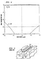
- FIGS. 3 and 4 are graphs representing the spectral responses of exemplary switches according to the invention, operated in the powered state.
- the switch of FIG. 3 is adapted for a peak response at 1.42 ⁇ m
- the switch of FIG. 4 is adapted for a peak response at 1.40 ⁇ m..
- FIG. 5 is a schematic drawing of a phase-shifting segment of the prior art that is bridge suspended in order to reduce its thermal coupling to the substrate.
- FIG. 6 is a schematic drawing of a phase-shifting segment according to the invention in one embodiment.
- a cavity underlying this phase-shifting segment reduces its thermal coupling to the substrate.
- FIG. 7 is a schematic drawing of an alternate phase-shifting segment underlain by a cavity to reduce its thermal coupling to the substrate.
- FIG. 8 is a graph representing the theoretical performance of a switch embodying the phase-shifting segment of FIG. 7. This graph shows the dependence of switch operating power and response time on the value of a geometrical parameter x , which partially describes the length of the decoupling cavity.
- an exemplary embodiment of our switch includes Y-branch coupler 10 having input port 20, MZI 30, and adiabatic 3-dB coupler 40.
- coupler 40 has an upper branch 50 with output port 60, and a lower branch 70 with output port 80.
- MZI 30 has an upper branch 90 and a lower branch 100.
- Branch 90 includes a phase-shifting segment 110 that can be heating by passing an activating electric current through metal film 120. This metal film is deposited over, e.g., the upper cladding of segment 110.
- an input signal P0 is applied to port 20. If the activating current is off, an output signal P1 appears at port 80 and little or no output appears at port 60. If the activating current is on, and is adjusted to produce a phase shift of 180° in segment 110, output signal P2 appears at port 60, and little or no output appears at port 80.
- FIG. 1 shows a phase-shifting metal film only on the upper branch
- a currently preferred switch includes a dummy film on the lower branch as well.
- the input coupler in an alternate embodiment of the inventive switch is adiabatic 3-dB coupler 130, having dual input ports 140 and 140'.
- adiabatic Y couplers can also be used in alternate embodiments.
- the Y-branch coupler, adiabatic 3-dB coupler, and MZI are constructed from planar waveguides. According to one well-known fabrication technique, these waveguides are formed from glass layers deposited on the surface of a silicon substrate.
- An exemplary fabrication sequence includes the steps of oxidizing the silicon surface to provide a lower cladding layer, depositing a core layer of phosophosilicate glass, lithographically patterning the core layer to define the waveguide configuration, and depositing an upper core layer of phosophosilicate glass. This technique is discussed generally in U.S. Patent No. 4,902,086, issued to C.H. Henry et al. on Feb. 20, 1990.
- An optical element including a MZI optically coupled to an adiabatic 3-dB coupler has been previously described in C.H. Henry, et al., "Analysis of Mode Propagation in Optical Waveguide Devices by Fourier Expansion," IEEE J. Quantum Electron. 27 (1991) 523 - 530.
- the element described there is a multiplexer. That is, turning again to FIG. 1, signals in separate wavelength channels entering the element through ports 60 and 80, respectively, are combined at port 20.
- the inventive switch has the different function of directing an input signal to one or the other of alternate output ports.
- This new function is achieved, in part, by adding phase-shifting segment 110 to the upper branch of the MZI.
- this switching function is effective over a relatively broad band of wavelengths.
- a switch designed to operate at 1.42 ⁇ m will typically be effective over a range of about 1.25 ⁇ m - 1.6 ⁇ m. Over this range, the switch response will typically drop by no more than about 0.2 dB from its peak value, as shown, e.g., in FIG. 3. Because the response of a correctly designed adiabatic 3 dB coupler is independent of wavelength (over typical operating ranges), this wavelength dependence is attributed to deviations of the phase shift away from 180° in the powered switch as the operating wavelength moves away from the peak wavelength.
- adiabatic 3-dB coupler 40 comprises a pair of waveguide branches 50, 70 that differ in width (measured in the direction parallel to the substrate surface and transverse to the propagation axis), but are otherwise equivalent.
- Coupler 40 includes a central portion 150 in which the separation between the branches is small enough to permit substantial optical coupling between them. (A typical separation is 2 - 3 ⁇ m.)
- the branches are flared apart in terminal portion 160, which is proximal the MZI, and in terminal portion 170, which is distal the MZI.
- the upper and lower branches are optionally tapered in portion 160, but in any case should be mutually symmetrical.
- the upper waveguide decreases in width in the propagation direction, and the lower waveguide increases in width (or vice versa ). From different widths at the point where portion 150 meets portion 170, these waveguides taper to equal widths at the point where portion 150 meets portion 160. In portion 170, the waveguides taper from respective, relatively small and relatively large widths to, typically, standard widths at the output ports 60 and 80. (The input ports of coupler 40, where coupler 40 meets the MZI, will also typically have standard widths.)
- the optical medium of the inventive switch supports a fundamental even mode and a first-order odd mode, and in operation, optical power will be concentrated in one or the other of these modes.
- Optical power admitted at input port 20 divides equally between the upper and lower arms of the MZI. If phase shifting segment 110 is not activated, these optical excitations recombine in such a way that the even mode is excited at point 180. If this occurs, then substantial output power appears only at port 80, which is associated with the wider waveguide. However, if there is a 180° phase shift in segment 110, the odd mode is excited. In this case, substantial output power appears only at port 60, which is associated with the narrower waveguide.
- the input coupler of the alternate embodiment of FIG. 2 is an adiabatic 3-dB coupler having dual input ports 140 and 140'. Optical power applied to either of these input ports divides equally between the upper and lower arms of the MZI. Consequently, this embodiment functions in a manner generally analogous to the single-input embodiment of FIG. 1. With no power to the heater (and thus no phase shift), the wide input will be coupled to the wide output, and the narrow input will be coupled to the narrow output. But with power applied, the wide input will be coupled to the narrow output, and vice versa .
- the performance of a single-input optical switch was predicted by computer simulations.
- the switch was designed for effective operation over a wavelength band including the 1.3- ⁇ m and 1.55- ⁇ m communication channels.
- the length of input coupler 10 measured along the general propagation axis of the switch, was 3 mm.
- the length of output coupler 40 was 11 mm.
- the length of the MZI was 9 mm, including upper parallel section 110 and lower parallel section 115, each 5 mm long. These sections were separated by 250 ⁇ m.
- Upper section 110 was heated by electric current passing through a resistive film such as a chromium film 3000 ⁇ thick and having a resistance of 820 ⁇ . Power dissipation of 0.44 W produced a rise in temperature of 13°C.
- the refractive index of section 110 increased with temperature at at rate of 10 ⁇ 5/°C.
- FIG. 3 is a graph showing the performance of the exemplary switch (neglecting intrinsic losses) operating with a 180° phase shift at 1.42 ⁇ m.
- the output signal P2 is shown as a transmission ratio in decibels. It is evident that losses due to power coupling into the undesired output arm of the switch are less than 0.1 dB over the desired operating range.
- FIG. 4 is a graph showing the performance of a similar switch operating with a 180° phase shift at 1.40 ⁇ m. Both the output signal P2 and the crosstalk (appearing at output P1) are shown. It is evident that crosstalk is less than -15 dB over a range of about 1.26 ⁇ m - 1.58 ⁇ m, and over that range, the P2 output falls no more than about 0.2 dB below its peak value.
- the electric power requirements of the phase-shifting segment are determined, in part, by the pattern of heat flow in the switch.
- the substrate can function as a heat sink.
- the power requirements tend to increase as thermal coupling to the substrate is increased.
- a phase-shifting segment with reduced thermal coupling to the substrate is described, e.g., in A. Sugita et al., "Bridge-Suspended Silica-Waveguide Thermo-Optic Phase Shifter and Its Application to Mach-Zehnder Type Optical Switch," Trans. IEICE E73 , (1990) 105 - 108.
- a bridge-suspended waveguide structure is formed by cutting grooves 200 adjacent the phase-shifting waveguide segment 210 that extend down to the substrate surface, and then etching recesses 220 in the substrate that partially underlie the waveguide segment. By performing this procedure on each side of the waveguide segment, the silicon base that supports the waveguide segment is reduced to a thin strip 230. This restricts thermal diffusion into the substrate, and consequently decreases power requirements.
- recess 240 is formed by etching from side 250 of the substrate, opposite the MZI waveguides. Some or all of the substrate material is removed from a region that underlies segment 110 and extends more than halfway between segment 110 and segment 115.
- etching methods will be apparent to those skilled in the art. For example, well-known methods of anisotropic etching are readily employed to form a recess having perpendicular walls in a (110) silicon substrate, or a recess having inclined walls (as shown in the figure) in a (100) silicon substrate. Alternatively, well-known isotropic etching methods are readily employed to form a recess having curved, concave walls in, e.g., a silicon or glass substrate.
- FIG. 8 is a graph showing the dependence of operating power and response time on the value of the parameter x in our computational model.
Landscapes
- Physics & Mathematics (AREA)
- Nonlinear Science (AREA)
- General Physics & Mathematics (AREA)
- Optics & Photonics (AREA)
- Optical Integrated Circuits (AREA)
- Optical Modulation, Optical Deflection, Nonlinear Optics, Optical Demodulation, Optical Logic Elements (AREA)
Applications Claiming Priority (2)
| Application Number | Priority Date | Filing Date | Title |
|---|---|---|---|
| US08/153,691 US5418868A (en) | 1993-11-17 | 1993-11-17 | Thermally activated optical switch |
| US153691 | 1993-11-17 |
Publications (1)
| Publication Number | Publication Date |
|---|---|
| EP0653665A1 true EP0653665A1 (fr) | 1995-05-17 |
Family
ID=22548320
Family Applications (1)
| Application Number | Title | Priority Date | Filing Date |
|---|---|---|---|
| EP94308238A Withdrawn EP0653665A1 (fr) | 1993-11-17 | 1994-11-09 | Commutateur optique à commande thermique |
Country Status (3)
| Country | Link |
|---|---|
| US (1) | US5418868A (fr) |
| EP (1) | EP0653665A1 (fr) |
| JP (1) | JPH07191351A (fr) |
Cited By (4)
| Publication number | Priority date | Publication date | Assignee | Title |
|---|---|---|---|---|
| EP0915511A2 (fr) * | 1997-10-31 | 1999-05-12 | Siemens Aktiengesellschaft | Dispositif comportant un substrat ayant une couche destinée a être chauffée |
| US6847750B1 (en) | 1999-12-07 | 2005-01-25 | Optun (Bvi) Ltd. | Thermo-optical waveguide switch |
| WO2005101115A1 (fr) * | 2004-04-19 | 2005-10-27 | Phoxtal Communications Ab | Commutateur optique |
| EP3047320A4 (fr) * | 2014-03-05 | 2016-09-07 | Huawei Tech Co Ltd | Commutateur thermo-optique intégré à piliers thermiquement isolés et restreignant la chaleur |
Families Citing this family (55)
| Publication number | Priority date | Publication date | Assignee | Title |
|---|---|---|---|---|
| JP3022181B2 (ja) * | 1994-03-18 | 2000-03-15 | 日立電線株式会社 | 導波路型光合分波器 |
| DE4427523C1 (de) * | 1994-08-03 | 1996-01-11 | Iot Integrierte Optik Gmbh | Asymmetrisches integriert-optisches Mach-Zehnder-Interferometer |
| US5630004A (en) * | 1994-09-09 | 1997-05-13 | Deacon Research | Controllable beam director using poled structure |
| US5623566A (en) * | 1995-05-19 | 1997-04-22 | Lucent Technologies Inc. | Network with thermally induced waveguide |
| US5623568A (en) * | 1995-09-15 | 1997-04-22 | Lucent Technologies Inc. | Compact and fabrication tolerant high speed digital optical Y-switches |
| US5640471A (en) * | 1995-12-28 | 1997-06-17 | Lucent Technologies Inc. | Adiabatic tapered S-bends for compact digital switch arrays |
| NL1003669C2 (nl) * | 1996-07-24 | 1998-01-28 | Nederland Ptt | Optisch niet-lineair vertakkingselement met MZ-interferometer. |
| US5889898A (en) * | 1997-02-10 | 1999-03-30 | Lucent Technologies Inc. | Crosstalk-reduced integrated digital optical switch |
| DE19717545A1 (de) * | 1997-02-27 | 1998-09-03 | Deutsche Telekom Ag | Optoelektronisches Bauelement mit räumlich einstellbarer Temperaturverteilung |
| US6389191B1 (en) | 1997-07-18 | 2002-05-14 | Jds Uniphase Inc. | Thermo-optical cascaded switch comprising gates |
| EP0905546A3 (fr) * | 1997-09-26 | 2002-06-19 | Nippon Telegraph and Telephone Corporation | Commutateur thermo-optique empilé, matrice de commutation et multiplexeur à insertion/extraction comprenant ce commutateur thermo-optique empilé |
| GB2320104B (en) * | 1997-10-16 | 1998-11-18 | Bookham Technology Ltd | Thermally isolated silicon layer |
| US6175671B1 (en) * | 1998-10-01 | 2001-01-16 | Nortel Networks Limited | Photonic crystal waveguide arrays |
| KR100326046B1 (ko) | 1999-06-21 | 2002-03-07 | 윤종용 | 열광학 스위치 및 그 제작방법 |
| US6351578B1 (en) | 1999-08-06 | 2002-02-26 | Gemfire Corporation | Thermo-optic switch having fast rise-time |
| AU1799501A (en) * | 1999-11-23 | 2001-06-04 | Nanovation Technologies, Inc. | Optical mach-zehnder switch having a movable phase shifter |
| AU4502201A (en) * | 1999-11-23 | 2001-06-04 | Nanovation Technologies, Inc. | Analog optical switch using an integrated mach-zehnder interferometer having a movable phase shifter |
| US7043134B2 (en) * | 1999-12-23 | 2006-05-09 | Spectalis Corp. | Thermo-optic plasmon-polariton devices |
| US6741775B2 (en) * | 2000-02-04 | 2004-05-25 | Fujikura Ltd. | Optical switch |
| US6658176B2 (en) | 2000-09-29 | 2003-12-02 | Sarnoff Corporation | Optical switch using movable micromechanical cantilevers and evanescent coupling |
| US6580850B1 (en) * | 2000-11-24 | 2003-06-17 | Applied Wdm, Inc. | Optical waveguide multimode to single mode transformer |
| JP3857925B2 (ja) * | 2001-04-11 | 2006-12-13 | 古河電気工業株式会社 | 光合分波器 |
| JP2003005232A (ja) * | 2001-04-18 | 2003-01-08 | Ngk Insulators Ltd | 光デバイス |
| US6816636B2 (en) | 2001-09-12 | 2004-11-09 | Honeywell International Inc. | Tunable optical filter |
| US20070133001A1 (en) * | 2001-09-12 | 2007-06-14 | Honeywell International Inc. | Laser sensor having a block ring activity |
| US7145165B2 (en) * | 2001-09-12 | 2006-12-05 | Honeywell International Inc. | Tunable laser fluid sensor |
| US7254299B2 (en) * | 2001-12-20 | 2007-08-07 | Lynx Photonic Networks, Inc. | High-tolerance broadband-optical switch in planar lightwave circuits |
| US20030118279A1 (en) * | 2001-12-20 | 2003-06-26 | Lynx Photonic Networks Inc | High-tolerance broadband-optical switch in planar lightwave circuits |
| US7470894B2 (en) * | 2002-03-18 | 2008-12-30 | Honeywell International Inc. | Multi-substrate package assembly |
| US20040071386A1 (en) * | 2002-04-09 | 2004-04-15 | Nunen Joris Van | Method and apparatus for homogeneous heating in an optical waveguiding structure |
| US7218814B2 (en) * | 2002-05-28 | 2007-05-15 | Optun (Bvi) Ltd. | Method and apparatus for optical mode conversion |
| US7609918B2 (en) * | 2002-05-28 | 2009-10-27 | Optun (Bvi) Ltd. | Method and apparatus for optical mode division multiplexing and demultiplexing |
| US7321705B2 (en) * | 2002-05-28 | 2008-01-22 | Optun (Bvi) Ltd. | Method and device for optical switching and variable optical attenuation |
| US6895157B2 (en) * | 2002-07-29 | 2005-05-17 | Intel Corporation | Thermal optical switch apparatus and methods with enhanced thermal isolation |
| US6961495B2 (en) * | 2003-01-27 | 2005-11-01 | Intel Corporation | Heating optical devices |
| US7902534B2 (en) * | 2004-09-28 | 2011-03-08 | Honeywell International Inc. | Cavity ring down system having a common input/output port |
| US7586114B2 (en) * | 2004-09-28 | 2009-09-08 | Honeywell International Inc. | Optical cavity system having an orthogonal input |
| US7656532B2 (en) * | 2006-04-18 | 2010-02-02 | Honeywell International Inc. | Cavity ring-down spectrometer having mirror isolation |
| US8111994B2 (en) * | 2006-08-16 | 2012-02-07 | Massachusetts Institute Of Technology | Balanced bypass circulators and folded universally-balanced interferometers |
| US7649189B2 (en) * | 2006-12-04 | 2010-01-19 | Honeywell International Inc. | CRDS mirror for normal incidence fiber optic coupling |
| WO2008118465A2 (fr) * | 2007-03-26 | 2008-10-02 | Massachusetts Institute Of Technology | Accord et commutation sans discontinuité de l'amplitude et des réponses en phase d'un résonateur optique |
| US7920770B2 (en) * | 2008-05-01 | 2011-04-05 | Massachusetts Institute Of Technology | Reduction of substrate optical leakage in integrated photonic circuits through localized substrate removal |
| US7663756B2 (en) * | 2008-07-21 | 2010-02-16 | Honeywell International Inc | Cavity enhanced photo acoustic gas sensor |
| US8198590B2 (en) * | 2008-10-30 | 2012-06-12 | Honeywell International Inc. | High reflectance terahertz mirror and related method |
| US7864326B2 (en) | 2008-10-30 | 2011-01-04 | Honeywell International Inc. | Compact gas sensor using high reflectance terahertz mirror and related system and method |
| WO2010065710A1 (fr) | 2008-12-03 | 2010-06-10 | Massachusetts Institute Of Technology | Modulateurs optiques résonants |
| WO2010138849A1 (fr) * | 2009-05-29 | 2010-12-02 | Massachusetts Institute Of Technology | Compensation de dynamique de cavité dans des modulateurs optiques résonnants |
| US8269972B2 (en) | 2010-06-29 | 2012-09-18 | Honeywell International Inc. | Beam intensity detection in a cavity ring down sensor |
| US8437000B2 (en) | 2010-06-29 | 2013-05-07 | Honeywell International Inc. | Multiple wavelength cavity ring down gas sensor |
| US8322191B2 (en) | 2010-06-30 | 2012-12-04 | Honeywell International Inc. | Enhanced cavity for a photoacoustic gas sensor |
| US8582929B2 (en) * | 2010-10-15 | 2013-11-12 | Northwestern University | Ultra-sensitive electric field detection device |
| CN103345023B (zh) * | 2013-07-17 | 2015-02-18 | 中国科学院半导体研究所 | 基于Mach-Zehnder光开关的四端口光学路由器 |
| WO2015096159A1 (fr) * | 2013-12-27 | 2015-07-02 | 华为技术有限公司 | Procédé de commande de signal optique, et procédé et dispositif de commande de matrice de commutation optique |
| US10142711B2 (en) * | 2015-04-14 | 2018-11-27 | International Business Machines Corporation | Low-crosstalk electro-optical Mach-Zehnder switch |
| CN107315224B (zh) | 2017-08-14 | 2018-09-28 | 河南仕佳光子科技股份有限公司 | 一种可调宽谱波长不灵敏定向耦合器 |
Family Cites Families (4)
| Publication number | Priority date | Publication date | Assignee | Title |
|---|---|---|---|---|
| CA2009352C (fr) * | 1989-02-07 | 1995-02-28 | Masao Kawachi | Elements de raccordement pour guides de lumiere et commutateurs optiques |
| EP0415225B1 (fr) * | 1989-09-01 | 1998-03-18 | Siemens Aktiengesellschaft | Dispositif optique intégré avec au moins un guide optique intégré sur un substrat semi-conducteur |
| JP2599488B2 (ja) * | 1990-02-26 | 1997-04-09 | 日本電信電話株式会社 | 光導波回路の特性調整方法およびその方法に使われる光導波回路 |
| NL9101835A (nl) * | 1991-11-01 | 1993-06-01 | Nederland Ptt | Geintegreerde optische component. |
-
1993
- 1993-11-17 US US08/153,691 patent/US5418868A/en not_active Expired - Lifetime
-
1994
- 1994-11-09 EP EP94308238A patent/EP0653665A1/fr not_active Withdrawn
- 1994-11-17 JP JP6307138A patent/JPH07191351A/ja active Pending
Non-Patent Citations (6)
| Title |
|---|
| KITOH T ET AL: "Novel broad-band optical switch using silica-based planar lightwave circuit", IEEE PHOTONICS TECHNOLOGY LETTERS, vol. 4, no. 7, July 1992 (1992-07-01), NEW YORK US, pages 735 - 737, XP000289298 * |
| LEMINGER O ET AL: "Adiabatically tapered directional coupling between dielectric waveguides", RADIO SCIENCE, vol. 26, no. 2, March 1991 (1991-03-01), USA, pages 579 - 582 * |
| OKUNO M ET AL: "8*8 optical matrix switch using silica-based planar lightwave circuits", IEICE TRANSACTIONS ON ELECTRONICS, vol. E76-C, no. 7, July 1993 (1993-07-01), JAPAN, pages 1215 - 1223, XP000394464 * |
| SHANI Y ET AL: "Integrated optic adiabatic devices on silicon", IEEE JOURNAL OF QUANTUM ELECTRONICS., vol. 27, no. 3, March 1991 (1991-03-01), NEW YORK US, pages 556 - 566, XP000227549 * |
| STEINBERG R A ET AL: "Performance limitations imposed on optical waveguide switches and modulators by polarisation", APPLIED OPTICS, vol. 15, no. 10, October 1976 (1976-10-01), NEW YORK US, pages 2440 - 2453, XP002263304, DOI: doi:10.1364/AO.15.002440 * |
| SUGITA A ET AL: "Bridge-suspended silica-waveguide thermo-optic phase shifter and its application to Mach-Zehnder type optical switch", TRANSACTIONS OF THE INSTITUTE OF ELECTRONICS AND COMMUNICATION ENGINEERS OF JAPAN, SECTION E, vol. E73, no. 1, January 1990 (1990-01-01), TOKYO JP, pages 105 - 108, XP000103975 * |
Cited By (6)
| Publication number | Priority date | Publication date | Assignee | Title |
|---|---|---|---|---|
| EP0915511A2 (fr) * | 1997-10-31 | 1999-05-12 | Siemens Aktiengesellschaft | Dispositif comportant un substrat ayant une couche destinée a être chauffée |
| EP0915511A3 (fr) * | 1997-10-31 | 2000-02-23 | Siemens Aktiengesellschaft | Dispositif comportant un substrat ayant une couche destinée a être chauffée |
| US6847750B1 (en) | 1999-12-07 | 2005-01-25 | Optun (Bvi) Ltd. | Thermo-optical waveguide switch |
| WO2005101115A1 (fr) * | 2004-04-19 | 2005-10-27 | Phoxtal Communications Ab | Commutateur optique |
| EP3047320A4 (fr) * | 2014-03-05 | 2016-09-07 | Huawei Tech Co Ltd | Commutateur thermo-optique intégré à piliers thermiquement isolés et restreignant la chaleur |
| US9448422B2 (en) | 2014-03-05 | 2016-09-20 | Huawei Technologies Co., Ltd. | Integrated thermo-optic switch with thermally isolated and heat restricting pillars |
Also Published As
| Publication number | Publication date |
|---|---|
| US5418868A (en) | 1995-05-23 |
| JPH07191351A (ja) | 1995-07-28 |
Similar Documents
| Publication | Publication Date | Title |
|---|---|---|
| US5418868A (en) | Thermally activated optical switch | |
| US6704487B2 (en) | Method and system for reducing dn/dt birefringence in a thermo-optic PLC device | |
| US7529455B2 (en) | Optical integrated device and optical control device | |
| Jinguji et al. | Two-port optical wavelength circuits composed of cascaded Mach-Zehnder interferometers with point-symmetrical configurations | |
| US6766083B2 (en) | Tunable coupler device and optical filter | |
| US7177502B2 (en) | Heating optical devices | |
| EP0980018A2 (fr) | Matériau polymérique et procédé pour la modulation et commutation optique | |
| EP2447761B1 (fr) | Attenuateur de lumiere variable de type a longueurs d'ondes | |
| US5623566A (en) | Network with thermally induced waveguide | |
| EP0987580A1 (fr) | Modulateur d'intensité lumineuse et commutateur le comprenant | |
| JP2005221999A (ja) | 光変調器及び光変調器アレイ | |
| CN114326164A (zh) | 一种基于相变材料的2×2光波导开关及其制备方法 | |
| CN115857201A (zh) | 一种基于薄膜铌酸锂密集双波导的偏振无关的电光调制器 | |
| US6925232B2 (en) | High speed thermo-optic phase shifter and devices comprising same | |
| WO2016051698A1 (fr) | Guide d'ondes optique du type à nervure et multiplexeur/démultiplexeur optique l'utilisant | |
| EP1259855A1 (fr) | Dispositif optique | |
| WO2002075978A1 (fr) | Interferometres optiques mach-zehnder a faible dependance de polarisation | |
| JPH08334639A (ja) | マッハツェンダ光回路 | |
| CN108627919B (zh) | 一种偏振不敏感的硅基光开关 | |
| CN113589556A (zh) | 光开关及其制作方法 | |
| CN112946826A (zh) | 一种基于soi材料制备的具有偏振旋转功能的热光开关 | |
| Takato et al. | Silica-based single-mode guided-wave devices | |
| US20030039447A1 (en) | Strip-loaded optical waveguide | |
| Takahashi et al. | High performance 8-arrayed 1× 8 optical switch based on planar lightwave circuit for photonic networks | |
| JPS63182608A (ja) | 導波形偏光分離素子 |
Legal Events
| Date | Code | Title | Description |
|---|---|---|---|
| PUAI | Public reference made under article 153(3) epc to a published international application that has entered the european phase |
Free format text: ORIGINAL CODE: 0009012 |
|
| AK | Designated contracting states |
Kind code of ref document: A1 Designated state(s): DE FR GB IT |
|
| 17P | Request for examination filed |
Effective date: 19951102 |
|
| 17Q | First examination report despatched |
Effective date: 19971205 |
|
| STAA | Information on the status of an ep patent application or granted ep patent |
Free format text: STATUS: THE APPLICATION IS DEEMED TO BE WITHDRAWN |
|
| 18D | Application deemed to be withdrawn |
Effective date: 19980416 |