EP0647326B1 - Dispersive microlens - Google Patents
Dispersive microlens Download PDFInfo
- Publication number
- EP0647326B1 EP0647326B1 EP93915465A EP93915465A EP0647326B1 EP 0647326 B1 EP0647326 B1 EP 0647326B1 EP 93915465 A EP93915465 A EP 93915465A EP 93915465 A EP93915465 A EP 93915465A EP 0647326 B1 EP0647326 B1 EP 0647326B1
- Authority
- EP
- European Patent Office
- Prior art keywords
- microlens
- blur spot
- dispersive
- microlenses
- color
- Prior art date
- Legal status (The legal status is an assumption and is not a legal conclusion. Google has not performed a legal analysis and makes no representation as to the accuracy of the status listed.)
- Expired - Lifetime
Links
- 238000000034 method Methods 0.000 claims abstract description 25
- 239000006185 dispersion Substances 0.000 claims description 46
- 238000003491 array Methods 0.000 claims description 22
- 230000003287 optical effect Effects 0.000 claims description 19
- 239000002131 composite material Substances 0.000 claims description 18
- 238000010276 construction Methods 0.000 claims description 14
- 230000003595 spectral effect Effects 0.000 claims description 11
- 238000004519 manufacturing process Methods 0.000 claims description 10
- 230000008569 process Effects 0.000 claims description 9
- 238000012545 processing Methods 0.000 claims description 9
- QNRATNLHPGXHMA-XZHTYLCXSA-N (r)-(6-ethoxyquinolin-4-yl)-[(2s,4s,5r)-5-ethyl-1-azabicyclo[2.2.2]octan-2-yl]methanol;hydrochloride Chemical compound Cl.C([C@H]([C@H](C1)CC)C2)CN1[C@@H]2[C@H](O)C1=CC=NC2=CC=C(OCC)C=C21 QNRATNLHPGXHMA-XZHTYLCXSA-N 0.000 claims description 7
- 230000002093 peripheral effect Effects 0.000 claims description 7
- 230000001419 dependent effect Effects 0.000 claims description 6
- 239000003086 colorant Substances 0.000 claims description 5
- 230000001172 regenerating effect Effects 0.000 claims description 4
- 239000012141 concentrate Substances 0.000 claims description 2
- 230000001276 controlling effect Effects 0.000 claims 1
- 230000002596 correlated effect Effects 0.000 claims 1
- 229920002120 photoresistant polymer Polymers 0.000 claims 1
- 238000009826 distribution Methods 0.000 description 26
- 239000000758 substrate Substances 0.000 description 7
- 238000003384 imaging method Methods 0.000 description 6
- 230000000750 progressive effect Effects 0.000 description 6
- 238000001228 spectrum Methods 0.000 description 6
- 239000000463 material Substances 0.000 description 5
- RPPBZEBXAAZZJH-UHFFFAOYSA-N cadmium telluride Chemical compound [Te]=[Cd] RPPBZEBXAAZZJH-UHFFFAOYSA-N 0.000 description 4
- 238000001816 cooling Methods 0.000 description 4
- 238000013461 design Methods 0.000 description 3
- 230000004438 eyesight Effects 0.000 description 3
- 230000010354 integration Effects 0.000 description 3
- XUIMIQQOPSSXEZ-UHFFFAOYSA-N Silicon Chemical compound [Si] XUIMIQQOPSSXEZ-UHFFFAOYSA-N 0.000 description 2
- 238000004458 analytical method Methods 0.000 description 2
- 230000008901 benefit Effects 0.000 description 2
- 239000013590 bulk material Substances 0.000 description 2
- 238000005530 etching Methods 0.000 description 2
- 229910052710 silicon Inorganic materials 0.000 description 2
- 239000010703 silicon Substances 0.000 description 2
- 230000004075 alteration Effects 0.000 description 1
- 230000015572 biosynthetic process Effects 0.000 description 1
- 238000006243 chemical reaction Methods 0.000 description 1
- 230000000694 effects Effects 0.000 description 1
- 239000000835 fiber Substances 0.000 description 1
- 239000012634 fragment Substances 0.000 description 1
- 230000004048 modification Effects 0.000 description 1
- 238000012986 modification Methods 0.000 description 1
- 230000005043 peripheral vision Effects 0.000 description 1
- 230000004044 response Effects 0.000 description 1
- 238000000926 separation method Methods 0.000 description 1
- 230000007480 spreading Effects 0.000 description 1
- 238000003892 spreading Methods 0.000 description 1
- 238000012360 testing method Methods 0.000 description 1
- 238000012546 transfer Methods 0.000 description 1
- 230000000007 visual effect Effects 0.000 description 1
Images











Classifications
-
- H—ELECTRICITY
- H10—SEMICONDUCTOR DEVICES; ELECTRIC SOLID-STATE DEVICES NOT OTHERWISE PROVIDED FOR
- H10F—INORGANIC SEMICONDUCTOR DEVICES SENSITIVE TO INFRARED RADIATION, LIGHT, ELECTROMAGNETIC RADIATION OF SHORTER WAVELENGTH OR CORPUSCULAR RADIATION
- H10F39/00—Integrated devices, or assemblies of multiple devices, comprising at least one element covered by group H10F30/00, e.g. radiation detectors comprising photodiode arrays
- H10F39/80—Constructional details of image sensors
- H10F39/806—Optical elements or arrangements associated with the image sensors
-
- G—PHYSICS
- G02—OPTICS
- G02B—OPTICAL ELEMENTS, SYSTEMS OR APPARATUS
- G02B27/00—Optical systems or apparatus not provided for by any of the groups G02B1/00 - G02B26/00, G02B30/00
- G02B27/10—Beam splitting or combining systems
- G02B27/1006—Beam splitting or combining systems for splitting or combining different wavelengths
-
- G—PHYSICS
- G02—OPTICS
- G02B—OPTICAL ELEMENTS, SYSTEMS OR APPARATUS
- G02B27/00—Optical systems or apparatus not provided for by any of the groups G02B1/00 - G02B26/00, G02B30/00
- G02B27/10—Beam splitting or combining systems
- G02B27/12—Beam splitting or combining systems operating by refraction only
- G02B27/123—The splitting element being a lens or a system of lenses, including arrays and surfaces with refractive power
-
- G—PHYSICS
- G02—OPTICS
- G02B—OPTICAL ELEMENTS, SYSTEMS OR APPARATUS
- G02B3/00—Simple or compound lenses
- G02B3/02—Simple or compound lenses with non-spherical faces
- G02B3/08—Simple or compound lenses with non-spherical faces with discontinuous faces, e.g. Fresnel lens
-
- G—PHYSICS
- G02—OPTICS
- G02B—OPTICAL ELEMENTS, SYSTEMS OR APPARATUS
- G02B5/00—Optical elements other than lenses
- G02B5/18—Diffraction gratings
- G02B5/1876—Diffractive Fresnel lenses; Zone plates; Kinoforms
-
- G—PHYSICS
- G02—OPTICS
- G02B—OPTICAL ELEMENTS, SYSTEMS OR APPARATUS
- G02B5/00—Optical elements other than lenses
- G02B5/18—Diffraction gratings
- G02B5/1876—Diffractive Fresnel lenses; Zone plates; Kinoforms
- G02B5/188—Plurality of such optical elements formed in or on a supporting substrate
- G02B5/1885—Arranged as a periodic array
-
- G—PHYSICS
- G02—OPTICS
- G02B—OPTICAL ELEMENTS, SYSTEMS OR APPARATUS
- G02B3/00—Simple or compound lenses
- G02B3/0006—Arrays
- G02B3/0037—Arrays characterized by the distribution or form of lenses
- G02B3/0056—Arrays characterized by the distribution or form of lenses arranged along two different directions in a plane, e.g. honeycomb arrangement of lenses
Definitions
- This invention relates to microlens arrays and associated detector/emitter pixel arrays.
- This invention relates particularly to dispersive microlens apparatus and methods which can be used in one mode for detecting multiple, different wavelengths from a bandwidth of the wavelengths (existing within an image plane blur spot) and which can be used in another mode for combining a plurality of different, emitted wavelengths into a bandwidth of the wavelengths (at a blur spot in an image plane).
- the individual microlenses of the present invention may typically range in size from a diameter of 50 microns to 1 millimeter.
- Related detectors may be fabricated from bulk material that is thinned to a thickness associated to fast optical design f ⁇ 1 in the substrates.
- the microlenses are located, usually in one dimensional or two dimensional arrays, at an image plane, and associated detectors/emitters are located in pixels in a detector/emitter plane which is spaced from the image plane.
- the individual microlenses of the present invention may be Fresnel or non-Fresnel microlenses, and may be fabricated by binary or non-binary fabrication techniques, may have a variety of geometric shapes, such as, for example, circular, square, hexagonal, and rhombic.
- PAJ-62293222 describes a colour display device including a microlens constructed to transmit and concentrate a selected bandwidth of light of a blur spot at the microlens to a smaller blur spot in a detector plane, and dispersion means for producing a dispersion of the bandwidth of the transmitted light and an elongated blur spot in which the wavelengths are varied from one end to the other end, the dispersive means comprising a grating formed integrally on the microlens.
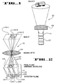
- Figure 1 is a side elevation view in cross section of an optical sensor system which utilizes dispersive microlens apparatus and methods of the present invention.
- Figure 2 is a diagrammatic view showing how each of three adjacent microlens has an individual instantaneous field of view (IFOV) and showing how the energy (or object) in that individual IFOV is transmitted to the detectors associated with the particular microlens.
- IFOV instantaneous field of view
- Figure 3 is an enlarged, schematic, fragmentary, isometric view showing how individual microlenses (in an array of microlenses located at an image plane) transmit energy and optical information (contained in individual blur spots in the image plane) to related individual pixels in a detector plane.
- Figures 4A, 4B and 4C are enlarged, fragmentary views, partly in cross section, showing how multiple detectors are associated with non-Fresnel dispersive microlenses (Fig 4A) and Fresnel dispersive microlenses (Figure 4B) and showing how a single detector is associated with a wide-band non-dispersive microlens ( Figure 4C).
- Figure 5 is an enlarged, fragmentary, plan view showing details of how, in detector arrays (without any associated micro-lenses) used prior to the present invention, two images in blur spots of two instantaneous fields of view could fall, at least in part, upon dead zones between the detectors.
- Figure 5 illustrates, in double cross hatched portions of one image, how a large portion of one image could be lost when there are dead zones between such prior art detectors.
- Figures 6 and 7 are related views showing, respectively, a fragmentary, enlarged plan view of a portion of the image plane and a fragmentary, enlarged view of a related portion of the detector plane.
- Figures 6 and 7 show how an image, or information, in a blur spot at the image plane is transferred to a much smaller area in a related pixel in the detector plane by a microlens positioned at the blur spot in the image plane.
- Figures 6 and 7 also show how a blur spot which spans four adjacent microlenses in the image plane can produce four, small fragments of that image in the four related pixels of the detector plane to conserve all of the energy in the image plane blur spot (when there is no dead zone between any of the four adjacent microlenses in the image plane, i.e. when there is a 100% fill factor).
- Figures 8A and 8B are elevation views showing how each individual microlens at a blur spot in the image plane reduces the size of the image transmitted to the detector plane so that there is space, or real estate, available at the detector plane which can be used for other purposes. Both Figures 8A and 8B show how micro cooling channels can be located in such available space in the pixels to provide cooling for adjacent heat producing components.
- Figure 8B shows how multiple detectors can be used in each unit pixel to obtain more than one signal from the information in a blur spot at the image plane when a dispersive microlens of the present invention is positioned at the image plane blur spot.
- Figures 9 and 10 are enlarged, fragmentary, plan views of a portion of the detector plane showing how multiple detectors can be located in individual pixels in the detector plane.
- Figure 9 shows two detectors in each pixel.
- Figure 10 shows three detectors in each pixel.
- Figures 11, 12 and 13 are related views showing how a dispersion producing surface configuration (Figure 11) is associated with a piano convex microlens ( Figure 12) to form a dispersive non-Fresnel microlens ( Figure 13) in accordance with one embodiment of the present invention.
- Figures 14, 15 and 16 show Fresnel counterparts to the respective Figures 11, 12 and 13 views.
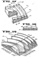
- Figure 17 is an isometric view of a dispersive, Fresnel microlens constructed in accordance with one embodiment of the present invention.
- the microlens shown in Figure 17 has a rectangular topology (is in the shape of a rectangle as viewed in plan view), and the transverse axis is not rotated with respect to the topology but is, instead, aligned and parallel with the related sides of the microlens.
- a portion of the central part of one end of the microlens has been broken away to show details of structure.
- Figure 18 is an elevation view, partly in cross section, taken along the line and in the direction indicated by the arrows 18-18 in Figure 17.
- FIG 19 is an isometric view of another embodiment of a dispersive Fresnel type microlens constructed in accordance with the present invention.
- the microlens shown in Figure 19 has a rectangular topology, like the microlens shown in Figure 17.
- the dispersive grating is perpendicular to the direction arrow 143.
- the microlens shown in Figure 19 differs from the microlens shown in Figure 17 in the fact that the microlens shown in Figure 19 is fabricated by a binary fabrication process while the microlens shown in Figure 17 is fabricated by a non-binary fabrication process.
- Figure 20 is a side elevation view of a dispersive non-Fresnel microlens and shows, in diagrammatic fashion in the lower part of the Figure, how the bandwidth of light existing in the blur spot in the image plane is transmitted through the dispersive microlens and is dispersed into individual wavelengths or individual wavebands A, B and C at specific locations on the detector plane.
- Figure 21 is an isometric view showing specific spectral lines of the distributions (the intensity levels and the area locations) of the dispersed wavelengths or wavebands on the detector plane for a dispersive non-Fresnel microlens like that shown in Figure 20.
- Figure 21 shows, by the height of the cones, the relative intensities of the specified dispersed wavelengths; and Figure 21 shows, by the areas occupied on the detector plane, the locations of the dispersed wavelengths.
- the alignment of the locations of the dispersed wavelengths shown in Figure 21 is a straight line which is canted at an angle with respect to the rectangular sides of the pixel shown in Figure 21. This angle results from a corresponding angle of skew of the related grating of the related microlens.
- the total bandwidth of the light transmitted through the dispersive non-Fresnel microlens of Figure 20 is distributed within the outer envelope indicated by the dashed outline in Figure 21; and the wavelength separation is in fact a continuum, rather than just the three separate cones shown for purposes of illustration in Figure 21.
- Figure 22 is an isometric view of a dispersive, non-Fresnel, binary fabricated microlens constructed in accordance with another embodiment of the present invention.
- the microlens shown in Figure 22 has a topology which is generally rectangular shaped, and the dispersion grating is not skewed.
- Figure 23 is an isometric view showing the spectrum distributions (the intensity levels and the area locations) of the dispersed wavelengths or wave bands on the pixel in the detector plane for the dispersive, non-Fresnel, binary microlens shown in Fig. 22.
- the bandwidth of light in the blur spot at the microlens in the image plane is dispersed to the smaller but elongated blur spot on the detector plane, and the wavelengths in the elongated blur spot in the pixel on the detector plane (as shown in Figure 23) are varied in a progressive way from one end of the blur spot to the other end.
- the total energies that fall on each detector area are obtained by a convolution, or integration, of the spectral blur spots and the responsivity function.
- the alignment of the dispersed wavelengths or wavebands in Figure 23 is a straight line which runs parallel to the sides of the pixel, and this alignment is produced by a zero skew of the dispersive grating of the non-Fresnel microlens as shown in Figure 22.
- Figures 24, 25 and 26 show the respective high distribution (red), medium distribution (green) and low distribution (blue) components existing in the elongated pixel blur spot shown in Figure 23. It should be noted that the terms red, green and blue are used here and throughout the text to refer to the distribution in the waveband discussed and not to specific colors as such.
- Figure 24 is an isometric view showing only the distribution (locations) and intensity levels of the longest (in this case red) wavelengths in the elongated pixel plane blur spot shown in Figure 23.
- Figure 25 is an isometric view showing only the distribution (locations) and intensity levels of the mid (in this case green) wavelengths of the elongated pixel plane blur spot shown in Figure 23.
- Figure 26 is an isometric view showing only the distribution (locations) and intensity levels of the shortest (in this case blue) wavelengths of the elongated pixel plane blur spot shown in Figure 23.
- Figure 27 is a side elevation view of a dispersive, Fresnel, non-binary microlens constructed in accordance with another embodiment of the present invention and shows, in diagrammatic fashion in the lower part of the figure, how the bandwidth of light existing in the blur spot at the microlens in the image plane is transmitted through the dispersive microlens and is dispersed into individual wavelengths or individual wavebands C, B and A at specific locations in a pixel on the underlying detector plane.
- Figure 28 is an isometric view showing the spectrum distributions (the intensity levels and the area locations) of the dispersed wavelengths or wavebands on the pixel in the detector plane for the dispersive, Fresnel, non-binary microlens shown in Figure 27.
- the bandwidth of light in the blur spot at the microlens in the image plane is dispersed to the smaller but elongated blur spot on the detector plane, and the wavelengths in the elongated blur spot in the pixel on the detector plane (as shown in Figure 28) are varied in a progressive way from one end of the blur spot to the other so that more than one wavelength can be detected and/or located within the elongated blur spot on the detector plane.
- the alignment of the dispersed wavelengths or wavebands in Figure 28 is a straight line which is skewed with respect to the sides of the pixel, and this alignment is produced by a corresponding skew axis of the dispersive grating of the Fresnel, non-binary microlens shown at Figure 27.
- Figure 29, 30 and 31 show the respective red (high distribution), green (medium distribution) and blue (low distribution) components existing in the elongated pixel blur spot shown in Figure 28.
- Figure 29 is an isometric view showing only distribution (locations) and intensity levels of the longest (in this case red) wavelengths in the elongated pixel plane blur spot shown in Figure 28.
- Figure 30 is an isometric view showing only the distribution (locations) and intensity levels of the mid (in this case green) wavelengths of the elongated pixel wavelengths of the elongated pixel plane blur spot shown in Figure 28.
- Figure 31 is an isometric view showing only the distribution (locations) and intensity levels of the shortest (in this case blue) wavelengths of the elongated pixel plane blur spots in Figure 28.
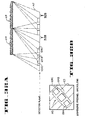
- Figure 32A is a side elevation view of two side by side dispersive, Fresnel, skewed dispersive grating, microlenses formed directly on one surface of the substrate. Each microlens is associated with three related detectors located in a correspondingly skewed blur spot in a related pixel on the opposite side of the substrate.
- Figure 32B is a bottom plan view, taken generally along the line and in the direction indicated by the arrows 32B--32B in Figure 32A.
- Figure 32B shows how the three detectors are aligned in the pixel in the detector plane for detecting the dispersed wavelengths or wavebands within the elongated blur spot indicated by the dashed outline in Figure 32B.
- Figure 33 is a side elevation view, generally like Figure 32A, but showing an embodiment in which two loop hole detectors are used in each pixel.
- the non-binary, non-Fresnel, dispersive microlenses shown in Figure 33 are fabricated in silicon and are mated to a frontside-illuminated detectors side as the loophole CdTe array.
- Figure 34A is an enlarged elevation view in cross section of one of the detectors of Figure 33.
- Figure 34B is an isometric view of the detector shown in Fig. 34A.
- Figures 35 and 36 are related views showing how two sets of detectors in a pixel in the detector plane can be specifically sized and positioned to pick up two different sets of signal information from the same overall color dispersed information contained within the elongated blur spot in the pixel in the detector plane.
- Figures 35 and 36 give a visual representation. The total energies that fall on each detector area are obtained by a convolution, or integration, of the spectral blur spots and the spectral responsivity functions.
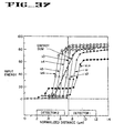
- Figure 37 is a graph showing the information obtained from the two different detectors positioned within an elongated blur spot in a single pixel by a convolution of the dispersed optical blur spot and detector responsivity function.
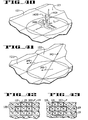
- Figure 38 is an isometric, fragmentary view showing an array of non-dispersive, non-binary, Fresnel microlenses which can be positioned in a peripheral part of the image plane.
- Figure 39 is an isometric view showing the spectral distributions (the intensity level and the area locations) of the wavelengths in the symmetrical spot formed on the detector plane by a non-dispersive microlens like one of the microlenses shown in Figure 38.
- Figure 39 illustrates how the higher order harmonics (extending orthogonally outwardly from the central cone for a square lens in Figure 39) produce an Airy disk pattern. This orthogonal pattern can produce resulting cross talk noise between adjacent pixels in the detector plane; because the patterns can be aligned, and the harmonics from one pattern can extend into and can add to the harmonics in an adjacent pixel.
- Figure 40 is an isometric, fragmentary view like Figure 39, but showing how an elongated blur spot formed in the pixel plane by a dispersive microlens in the image plane can also produce higher order harmonics in the pixel which can extend orthogonally into and in alignment with harmonics in adjacent pixels to produce cross talk noise.
- Figure 41 shows how a diagonally skewed dispersion grating angle can result in a diagonal alignment of higher order harmonics which can still result in cross talk noise between diagonally adjacent pixels in the pixel plane.
- Figure 42 shows a topology for square microlenses with a diagonal skew angle of the dispersion grating which is effective to eliminate orthogonal cross talk noise but which can still result in diagonal cross talk noise between diagonally adjacent pixels.
- Figure 43 shows a topology in which rectangular shaped microlenses, each having a diagonal skew angle of the dispersion grating, can be longitudinally offset or staggered in adjacent rows to eliminate any diagonal cross talk noise between diagonally adjacent pixels in the detector plane.
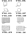
- Figures 44, 45, 46 and 47 show configurations for microlenses.
- Figure 44 shows a rectangular configuration
- Figure 45 shows a rhombic, trapezoidal configuration.
- Figure 46 shows a hexagonal configuration. This configuration has a number of advantages for maximizing the concentration and distribution of information in a related detector plane.
- Figure 47 shows a circular configuration for a microlens.
- Figure 48 shows a microlens array in which the individual microlenses are circular microlenses.
- Figure 49 shows a microlens array in which the individual microlenses have a rhombic configuration.
- Figure 50 shows a microlens array in which the individual microlenses have a hexagonal configuration.
- Figure 51 shows a microlens array in which each individual microlens has a rectangular configuration and in which each microlens in each row is offset with respect to the microlenses in adjacent rows.
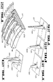
- Figure 52 is an elevation view of a rectangular, Fresnel, binary, dispersive microlens constructed in accordance with an embodiment of the present invention.
- Figure 53 is a diagrammatic plan view of the microlens shown in Figure 2 and shows the dispersion grating having a zero skew angle (as indicated by the direction arrow 143 which is perpendicular to the grating).
- Figure 54 is a top plan photograph (generated by a scanning electron microscope -- SEM) of the fabricated dispersive microlens shown in Figures 52 and 53.
- Figure 55 is a top plan SEM photograph showing a fabricated array of microlenses made up of individual microlenses each having the construction shown in Figure 54.
- Figure 56 is a diagrammatic plan view, like Figure 53, but showing a rectangular microlens having the dispersion grating skewed at an angle perpendicular to the direction arrow 143 in Figure 56.
- Figure 57 is a top plan SEM photograph of the fabricated dispersive microlens shown in Figure 56 and embodying the Fresnel, binary construction shown in Figure 52.
- Figure 58 is a top plan view of four pixels in a detector plane, offset in adjacent rows, to correspond to the offset of related rectangular microlenses like the microlens shown in 57, and showing the location of the elongated blur spot in each pixel as produced by the microlens construction shown in Figure 57.
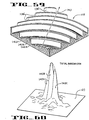
- Figure 59 is an isometric view of a dispersive, Fresnel microlens like that shown in Figure 57.
- Figure 59 shows a dispersive, rectangular-shaped, binary fabricated, Fresnel microlens having the dispersion grating skewed at the angle indicated by the direction arrow in Figure 59.
- Figure 60 is an isometric view (similar to Figure 21) showing specific spectral lines of the distributions (the intensity levels and the locations) of dispersed wavelengths on the pixel in the detector plane for the dispersive, Fresnel, binary microlens shown in Figure 59.
- the illustrated spectral blur spots are typical (blue, green, red) and are related to the lambda-low to lambda-high continuum within the total bandwidth (indicated by the dashed outline in Figure 60).
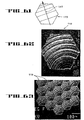
- Figure 61 is a schematic plan view showing a hexagonal shaped microlens having a dispersion grating inclined at the angle indicated by the direction arrow in Figure 61.
- Figure 62 is a plan SEM photograph of a fabricated low dispersive, binary, Fresnel, hexagonal shaped microlens having the dispersion grating inclined at the angle indicated in Figure 61.
- Figure 63 is a top plan SEM photograph of a fabricated test array of hexagonal shape microlenses having the structure of the microlens shown in Figure 62.
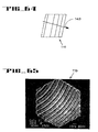
- Figure 64 is a fragmentary, plan view showing a rhombic shaped microlens having a dispersion grating skewed at the angle perpendicular to the direction arrow in Figure 64.
- Figure 65 is a top plan SEM photograph of a fabricated high dispersive, hexagonal shaped, binary fabricated, Fresnel microlens having a dispersion grating skewed at the angle perpendicular to the direction arrow 143 in Figure 64.
- Figure 66 is a top plan view of a composite array of pixels located at the detector plane and comprising a high resolution, (multicolor) pixel array of hexagonal shaped pixels in the central part of the composite array and having a lower resolution (wideband) pixel array of pixels in the peripheral part of the array.
- a high resolution, (multicolor) pixel array of hexagonal shaped pixels in the central part of the composite array and having a lower resolution (wideband) pixel array of pixels in the peripheral part of the array.
- multicolor and/or wideband may be a particular choice for a particular application.
- the high resolution region in combination with a low resolution region is often a more fundamental issue.
- Figure 67 is an isometric, fragmentary, enlarged view showing a composite array of microlenses in an image plane for association with the composite array of pixels shown in Figure 66.
- High resolution, dispersive, hexagonal microlenses comprise the central part of the composite microlens array; and non-dispersive, low resolution, wideband microlenses make up the outer peripheral part of the composite microlens array.
- Figure 68 is an elevation view showing how three emitters (each emitting a specified wavelength of color --red, green and blue) are arranged in alignment within an axially skewed, elongated blur spot in a pixel in the pixel plane and are associated with a related, same skew angle of dispersive grating, microlens in an image plane for combining the three separate wavelengths or wavebands of light emitted by the three emitters into a bandwidth of light at a blur spot existing at the location of the dispersive microlens in the image plane.
- the color content and intensity in the bandwidth of the light in the blur spot at the microlens are dependent upon the relative intensities of the different wavelengths emitted by the three emitters in the detector plane.
- Figure 69 is a bottom plan view taken along the line and in the direction indicated by the arrows 69-69 in Figure 68.
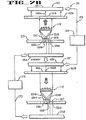
- Figure 70 is a diagrammatic view showing how the dispersive lens of the present invention is used in one (color combining) mode for combining a plurality of different, emitted wavelengths (emitted from emitters in an emitter plane) into a bandwidth of the wavelengths (at a blur spot in an image plane) and is used in another (color detecting) mode for detecting multiple different wavelengths (by detectors at a detector plane) from a bandwidth of wavelengths (existing within an image plane blur spot) so as to enable color information not only to be emitted and combined but also to be dispersed and detected for color transmitting and regenerating methods and apparatus, such as, for example, color television, color recording, color facsimile and color printing processes and apparatus.
- color combining for combining a plurality of different, emitted wavelengths (emitted from emitters in an emitter plane) into a bandwidth of the wavelengths (at a blur spot in an image plane) and is used in another (color detecting) mode for detecting multiple different wavelengths (by detectors at
- the present invention relates to dispersive microlens apparatus and methods which can be used in a detecting mode for dispersing and detecting multiple different wavelengths or wavebands from a bandwidth of the wavelengths existing within an image plane blur spot) and which can also be used in a combining mode (for combining a plurality of different, emitted wavelengths into a bandwidth of the wavelengths at a blur spot in an image plane).
- FIGS 1 and 2 of the drawings illustrate object imaging environments in which the dispersive microlens apparatus and methods of the present invention are utilized to perform complex object imaging and analysis operations.
- Figures 68, 69 and 70 of the drawings illustrate color combining environments in which the dispersive microlens apparatus and methods of the present invention are used for combining a plurality of different, emitted wavelengths into a bandwidth of wavelengths at a blur spot in an image plane.
- Figure 70 illustrates how the dispersive microlens apparatus and methods enable color information not only to be dispersed, separated and detected but also to be emitted and combined for color transmitting and regenerating applications, such as, for example, color television, color recording, color facsimile and color printing processes and apparatus.
- the dispersive microlens in the first mode (the mode for detecting multiple different wavelengths or wavebands from a bandwidth of the wavelengths) will be described first and will be described with reference to use in a sensor environment of the general kind shown in Figures 1 and 2.
- Figure 1 shows a sensor system, indicated generally by the reference numeral 101, which can be used for imaging/detecting an object and which can also provide (by use of the dispersive microlens apparatus and methods of the present invention) real time discrimination of sensed optical information for certain other qualities, such as, for example, color and/or temperature, of the object or objects generating the optical information.
- a sensor system indicated generally by the reference numeral 101, which can be used for imaging/detecting an object and which can also provide (by use of the dispersive microlens apparatus and methods of the present invention) real time discrimination of sensed optical information for certain other qualities, such as, for example, color and/or temperature, of the object or objects generating the optical information.
- the sensor system 101 includes imager optics 109, focal plane arrays 111 (comprising microlens arrays and detector arrays), and a signal processing unit 113.
- Figure 2 is a diagrammatic view showing how each of three adjacent microlens 119 has an individual instantaneous field of view (IFOV-1, IFOV-2 and IFOV-3) and showing how the energy (or object) in that individual IFOV is transmitted to the detectors (124A and 124B) associated with the particular microlens.
- IFOV-1, IFOV-2 and IFOV-3 an individual instantaneous field of view
- Figure 3 is an enlarged, diagrammatic view which illustrates details of the focal plane arrays 111 shown in Figures 1 and 2.
- the focal plane arrays 111 in Figure 3 comprise a microlens array 115 in an image plane and a pixel array 117 in a detector plane.
- microlens array 115 at the image plane in the focal plane arrays 111 allows the concentration of incident irradience to a small fraction of the pixel area in the detector plane.
- the microlens array 115 in one embodiment of the invention is a composite array which comprises a central (foveal vision) array of high resolution, dispersive, individual microlenses 119 surrounded by an outer, peripheral array of non-dispersive, low resolution, wideband, individual microlenses 121.
- a central (foveal vision) array of high resolution, dispersive, individual microlenses 119 surrounded by an outer, peripheral array of non-dispersive, low resolution, wideband, individual microlenses 121.
- different combinations of high and low resolution regions may be used and different combinations of dispersive and non-dispersive microlens may be used.
- the pixel array 117 contains a plurality of pixels with each individual pixel related to a corresponding individual microlens in the microlens array 115.
- high resolution (multicolor) pixels 123 are located in the central part of the composite pixel array 117 and lower resolution (wideband) pixels 126 are located in the peripheral part of the composite pixel array 117.
- an instantaneous field of view IFOV
- any object or objects within that instantaneous field of view are imaged into an individual blur spot 125 at the location of an individual microlens 119 at the image plane.
- the optical information within this blur spot is transmitted through the microlens 119 to a related pixel 123 in the detector plane.
- one or more detectors 124 are positioned within each pixel in the detector plane for receiving a signal or signals from the reduced size pixel blur spot.
- Figures 4A, 4B and 4C are enlarged, fragmentary views, partly in cross section, showing how multiple detectors are associated with non-Fresnel dispersive microlenses (Figure 4A) and Fresnel dispersive microlenses (Figure 4B) and showing how a single detector is associated with a wideband Fresnel, non-dispersive microlens ( Figure 4C).
- Figure 5 shows a detector plane used without an associated micro-optics array.
- An object 127 within a blur spot 125 which falls substantially fully upon a related detector 124 would have substantially all of the energy and information within that object transmitted to a corresponding component in the signal processing unit 113; so a dead zone between adjacent detectors would not have too much significance with respect to the object 127.
- the present invention includes micro-optics above the detector plane array. As will be more clear from the description to follow, this use of the microlenses permits the detectors to be spaced apart from one another without any problems of dead zone losses as described immediately above in reference to the previously used Figure 5 detector array construction.
- the preferred construction is to have all of the microlenses in the microlens array immediately adjacent one another so as not to have any optically dead space between any of the microlenses.
- Figure 6 shows such construction for square shaped (in plan), Fresnel-type microlenses 121.
- Figure 6 and related Figure 7 illustrate how all of the optical information within each individual blur spot 125 is preserved and is transmitted to detectors 124 in pixels 123 in the detector plane, even when a blur spot spans more than one individual microlens in the microlens array 115.
- the object image 129 which falls on four adjacent microlenses 121 is fully transmitted to four detectors 124 in the four related pixels 123 (see Figure 7) in the detector plane.
- each individual microlenses in the course of transferring the optical information at an image plane blur spot into a smaller detector plane blur spot in a related pixel in the detector plane, is effective to produce a high contrast ratio, high fill factor and high optical gain of the optical information in the detector plane blur spot with respect to any existing, unwanted noise (produced by large detector elements) which may be present at the detector plane.
- the optical gain achieved is the area ratio of the microlens to the detector (see Figure 8A).
- the microlens array 115 and pixel array 117 provide high overall optical efficiency, nearly 100% fill factor, extended wavelength response and reduced detector noise levels.
- Microlenses constructed in accordance with the present invention may typically range in size from a diameter D of 50 microns to 1000 microns, and the related detectors may be fabricated from bulk material that is thinned to a thickness t that represents an f ⁇ 1 lens.
- the small detector plane blur spots (corresponding generally to the diameter d of the detector 124 shown in Figure 8A) leave relatively large adjacent areas, or real estate, in the detector plane which can be used for other purposes.
- micro cooling channels 133 can be positioned in the relatively large adjacent areas and used for cooling nearby structure.
- the available real estate may also be utilized for analog signal processing circuits, such as, for example, the analog circuits 126 in Figures 8A and 8B.
- the circuits can be conventional detector read-out circuits, detector signal adding circuits or ratio-ing circuits, as the system design requires.
- multiple detectors such as the detectors 124A, 124B and 124C shown in Figure 8B, can be positioned in a number of locations and in a variety of alignments within each individual pixel. Having the space available to do this in a detector plane pixel is a benefit which is of particular utility in connection with a dispersive microlens like the dispersive, high resolution microlens 119 shown in Figure 8B, as will be described in more detail below.
- Figure 9 is a fragmentary plan view which shows how two detectors 124A and 124B can be positioned (in this case orthogonally) in each unit pixel 123.
- Figure 10 is a fragmentary top plan view showing how three detectors 124A, 124B and 124C may be positioned within each unit pixel 123.
- the blur spot 125 results from a combination of refraction and diffraction.
- the blur resulting from refraction results from the different focus of different wavelengths.
- the blur caused by diffraction is inherent to a certain degree in all refractive (geometric optics) lenses.
- This blur spot phenomenon which results primarily from refraction (geometric optics) and, to a much lesser extent, diffraction (wave optics) of lenses is described at pages 727 and 728 of Physics by Hausmann and Slack, 3rd edition, 1948, and published by D. Van Nostrand Company, Inc., New York. These pages of this reference are incorporated by reference in this application.
- a microlens (1) is constructed to transmit a selected bandwidth of light existing in the incident blur spot at the microlens plane 115 to a smaller pixel blur spot in a pixel plane 117 spaced at a selected distance from the microlens and (2) includes dispersion means for producing both a controlled dispersion of the bandwidth of light (as the light is transmitted to the smaller blur spot) and also an elongated shape of the smaller pixel blur spot (in which the elongated shape wavelengths or wavebands are varied in a progressive way from one end of the elongated blur spot to the other so that more than one wavelength can be detected and/or located within the elongated blur spot).
- the dispersion means comprise a configured surface formed integrally on the microlens.
- Figures 11, 12 and 13 are related views showing how a dispersion producing surface configuration (Figure 11) can be visualized as being combined with a plano convex surface configuration microlens ( Figure 12) to form a single, combined surface, dispersive non-Fresnel microlens ( Figure 13) in accordance with one embodiment of the present invention.
- the dispersion producing means 135 may be visualized as a series of identically sized, identically spaced, individual prism surfaces each having an inclined surface 136 and a vertical surface 138.
- the prism surfaces are aligned in a grating arrangement (an arrangement in which corresponding surfaces on corresponding prisms extend parallel to one another).
- the prism surfaces are effective to produce dispersion substantially entirely by geometric refraction (and not to any significant extent by the wave optics diffraction of a diffraction grating).
- the grating arrangement shown in Figure 11 is a grating in the general sense of the term. That is, the arrangement of the prismatic surfaces, when viewed from above, can have the appearance of parallel elements, like a grating of latticed bars set in a window, door, etc.
- the use of the term grating with reference to the construction shown in Figure 11 is not a reference to a grating as an optical diffraction grating.
- the grating shown in Figure 11 does not produce slits equally spaced which can cause dispersion by spreading of a wave into its component frequencies.
- the grating arrangement shown in Figure 11 instead essentially causes dispersion of the light by causing different wavelengths of the light to be transmitted through the material of the microlens at different velocities. There is, of course, always some diffraction which is caused by the material of the lens itself. In this regard, see the above discussion of the formation of the blur spot 125 and the reference to pages 727 and 728 of Physics by Hausmann and
- Figure 12 shows a plano convex microlens 137 having a convex surface 140.
- dispersive microlens 119 shown in Figure 13 is obtained.
- the curved surfaces 142 of the dispersive microlens 119 have curvatures which are a combination of the curvature 140 of Figure 12 and the inclination of the prismatic surfaces 136 shown in Figure 11.
- the surfaces 138 shown in Figure 13 correspond to the surfaces 138 shown in Figure 11 for producing the prism effects.
- Figures 14, 15 and 16 are related views showing how a dispersion producing surface configuration 135 (Figure 14) is associated with a Fresnel-type piano convex microlens 139 ( Figure 15) to form a dispersive Fresnel microlens 119 ( Figure 16) in accordance with another embodiment of the present invention.
- Figure 17 is an isometric view of a dispersive, Fresnel microlens 119 constructed in accordance with one embodiment of the present invention.
- the dispersive microlens 119 shown in Figure 17 is basically like the lens shown in Figure 16 but is shown (in Figure 17) mounted on a substrate 141.
- the substrate 141 may be a separate material if required for a particular optomechanical application, or the substrate 141 may be common for the lenses on one side and the detectors on the other side (back illuminated detectors).
- the microlens 119 shown in Figure 17 has a rectangular topology (is in the shape of a rectangle as viewed in plan view), and the grating is not skewed with respect to the topology but is instead, aligned and parallel with the related sides of the microlens.
- a portion of the central part of one end of the microlens has been broken away to show details of structure.
- Figure 18 is an elevation view, partly in cross section, and is taken along the line and in the direction indicated by the arrows 18-18 in Figure 17.
- the dispersive, Fresnel microlens shown in Figure 17 is fabricated by non-binary techniques.
- Figure 19 shows a dispersive, Fresnel microlens having a rectangular, square topology and a non-skewed grating angle (all similar to the microlens shown in Figure 17), but the microlens 119 shown in Figure 19 is fabricated by a binary fabrication process.
- the angle of the dispersive grating is perpendicular to the direction arrow 143 in Figure 19.
- Figure 19 shows, in the dashed outline beneath the direction grating arrow 143, the cross section configuration of the Fresnel-type dispersive microlens in that part of the microlens.
- the vertical wall surfaces 138 which form part of the dispersion grating are curved surfaces (as viewed in plan) rather than straight lines.
- the surfaces 142 are not smoothly curved (like the smoothly curved surfaces 142 shown in Figure 17) but are instead formed as a series of discrete levels 142A, 142B, 142C, 142D, 142E and 142F.
- the dispersive microlens of the present invention transmits a selected bandwidth of light (existing in the incident blur spot 125 at the microlens) to a much smaller pixel blur spot in a plane space at a selected distance from the microlens.
- This much smaller pixel blur spot is indicated in Figure 20 by the reference numeral 145.
- the blur spot 145 is shown, for easier viewing, larger than and out of scale to the actual ratio of diameters D (at the image plane) to d (at the detector plane).
- the dispersive means on the microlens produce both a controlled dispersion of the bandwidth of the light (as the light is transmitted to a smaller pixel blur spot) and also an elongated shape of the smaller pixel blur spot.
- the wavelengths or wavebands in the elongated pixel blur spot are varied in a progressive way from one end of the elongated blur spot to the other so that more than one wavelength can be detected and/or located within the elongated blur spot.
- Figures 20 and 21 illustrate how the bandwidth of light existing in the blur spot 125 (see Figure 6) at the microlens 119 in the image plane is transmitted (see the illustrative light rays indicated by the dashed lines in Figure 20) through the dispersive microlens and is dispersed into individual wavelengths or wavebands 145A, 145B and 145C within the elongated detector plane blur spot 145 at specific locations on the detector plane.
- Figure 21 is an isometric view showing selected wavelengths from the spectrum distributions (the intensity levels and the area locations) of the dispersed wavelengths or wavebands 145A, 145B and 145C on the detector plane pixel 123 for a dispersive, non-Fresnel microlens like that shown in Figure 20.
- Figure 21 shows, by the height of the cones 145A (blue), 145B (green) and 145C (red), the relative intensities of the dispersed wavelengths or wavebands.
- blue, green and red is a use to indicate the low, medium and high wavelengths from the spectral band existing in the blur spot.
- the use of the terms is not intended to refer to specific, visible colors as such.
- Figure 21 shows, by the areas occupied (by the basis of the cones 145A, 145B and 145C) on the detector plane, the locations of the dispersed wavelengths or wavebands.
- the alignment of the locations of the dispersed wavelengths or wavebands 145A (blue), 145B (green), and 145C (red) shown in Figure 21 is a straight line which is canted at an angle with respect to the rectangular sides of the pixel 123 shown in Figure 21. This angle results from a corresponding angle of skew of the related grating of the related microlens 119 shown in Figure 20.
- Figure 22 is an isometric view of a dispersive, non-Fresnel binary fabricated microlens constructed in accordance with another embodiment of the present invention.
- the microlens 119 in Figure 22 has a topology which is generally square shaped, and the axis of the dispersion grating is aligned with the sides of the microlens so that there is no skew to this axis.
- the dashed lines in Figure 22 show the cross sectional configuration of the microlens at the locations of the dashed lines.
- Figure 23 is an isometric view showing the spectrum distributions (the intensity levels and the area locations) of the dispersed wavelengths or wavebands on the pixel 123 in the detector plane for the dispersive, non-Fresnel, binary microlens 119 shown in figure 22.
- the bandwidth of light in the blur spot 125 at the location of the microlens 119 in the image plane is dispersed to the smaller but elongated blur spot 145 on the detector plane.
- the wavelengths in the elongated blur spot 145 in the pixel 123 on the detector plane are varied in a progressive way from one end of the pixel plane blur spot to the other so that more than one wavelength can be detected and/or located within the elongated blur spot 145 on the detector plane.
- the elongated blur spot is dispersed into the respective components 145A (blue), 145B (green), and 145C (red) components as shown in Figure 23.
- the alignment of the dispersed wavelengths or wavebands of the pixel plane blur spot 145 in Figure 23 is a straight line which runs parallel to the sides of the pixel 123, and this alignment is produced by a zero angle skew of the dispersive grating on the non-Fresnel microlens 119 shown in Figure 22.
- Figures 24, 25 and 26 show the respective red, green and blue components existing in the elongated pixel plane blur spot shown in Figure 23.
- Figure 24 is an isometric view showing only the distribution (location) and intensity levels of the longest (in this case red) wavelengths in the elongated pixel plane blur spot shown in Figure 23.
- Figure 25 is an isometric view showing only the distribution (location) and intensity levels of the mid (in this case green) wavelengths in the elongated pixel plane blur spot shown in Figure 23.
- Figure 26 is an isometric view showing only the distribution (locations) and intensity levels of the shortest (in this case blue) wavelengths of the elongated pixel plane blur spot shown in Figure 23.
- Figure 27 is a side elevation view of a dispersive, Fresnel, non-binary, skewed grating axis, microlens 119 constructed in accordance with another embodiment of the present invention.
- Figure 28 is an isometric view (generally similar to the isometric view shown in Figure 23) showing the spectrum distributions (the intensity levels and the area locations) of the dispersed wavelengths or wavebands 145A (blue), 145B (green), and 145C (red) which make up the elongated pixel plane blur spot 145 produced by the microlens 119 shown in Figure 27.
- the alignment of the dispersed wavelengths or wavebands in Figure 28 is a straight line which is skewed with respect to the sides of the pixel 123, and this alignment is produced by a corresponding skew axis of the dispersive grating of the microlens 119 shown in Figure 27.
- Figures 29, 30 and 31 show the respective red, green and blue components existing in the elongated pixel plane blur spot 145 shown in Figure 28.
- dispersive microlens 119 and associated detectors 124 can be structured in accordance with the present invention.
- Figures 32A and 32B show one way, and Figures 33, 34A and 34B show another way.
- dispersive, Fresnel, microlenses with rotated grating 119 are formed directly on one surface of a commercially available cadmium tellurium (CdTe) substrate 147.
- CdTe cadmium tellurium
- Figure 33 shows how a dispersive, non-Fresnel, microlenses 119 fabricated in silicon (Si) is mated to a frontside-illuminated, commercially available, loophole array of two CdTe detectors 124A and 124B in each pixel plane blur spot 145.
- one detector 124A can be used to detect one bandwidth of colors in the elongated pixel plane blur spot 145 and another detector 124B can be used to detect another, different bandwidth of colors within the elongated pixel plane blur spot 145.
- the constructions shown in Figures 32A, 32B and 33 are illustrated as monolithic integration constructions, but (for clarity of illustration in the drawing views) the material between the dispersive microlenses and the detectors has been left clear rather than crosshatched.
- the dispersive microlens of the present invention disperses the component wavelengths or wavebands of light within the elongated pixel plane blur spot 145 in a progressive way and at exact locations in the pixel plane blur spot, a plurality of detectors can be positioned at particular locations within the elongated blur spot to detect specific signals which are dependent upon the locations of the detectors in the pixel plane blur spot. This feature of the present invention is best illustrated in Figures 35 and 36.
- Figures 35 and 36 are related views showing how two sets of detectors in a pixel 123 in the detector plane can be specifically sized and positioned to pick up two different sets of signal information from the same overall color dispersed information contained within the elongated blur spot 145 in the pixel 123 in the detector plane.
- the particular selection chosen is system dependent.
- the uses of the two sets of detectors illustrated in Figures 35 and 36 permit the pick-up of two different sets of signal information from the long, medium and short wavelengths within any given bandwidth.
- the illustrated band is long wavelength infrared (LWIR) in the 8-12 micron bandwidth.
- This 8-12 LWIR is an example. Similar results may be generated in other wavelength bands, i.e., visible (Vis) near infrared (NWIR), short infrared (SWIR), mid infrared (MWIR) region.
- Vis visible
- NWIR near infrared
- SWIR short infrared
- MWIR mid infrared
- Figure 35 shows how one detector 124A is sized and positioned to pick up a signal which is representative of the energy contained within both the 145C (red, 12 micron) wavelength and the 145B (green, 10 micron) wavelength while the other detector 124B is sized and positioned to pick up a signal which is representative of the energy primarily within the 145A (blue, 8 micron) wavelength of the elongated detector plane blur spot 145.
- the dispersive microlens which produces the elongated blur spot 145 is a 100 micrometer square, Fresnel microlens having a rotated grating which is rotated to an angle of 14 degrees (perpendicular to the line indicated by the direction arrow 143).
- Grating rotation/canting angle is selected from a design requirement to minimize optical crosstalk between neighboring pixels.
- the microlens was fabricated by a binary fabrication process utilizing two photolitho-graphic and anisotropic etching steps.
- the resulting blur spot 145 shown in Figure 35 is basically like that illustrated in Figure 28 of the drawings.
- Figure 36 shows how a different set of signals can be obtained (from the same pixel plane blur spot as shown in Figure 35) by using a set of detectors which are positioned at locations different from the set of detectors shown in Figure 35.
- the detector 124A is sized and positioned to pick up a signal which represents all of the energy contained within the 145C portion (the red, 12 micron) wavelength and part of the energy contained within the longer wavelength end of the 145B portion (the red-green, 11 micron) wavelengths.
- the other detector 124B is positioned to pick up a signal which is representative of all of the information contained within the portion 145C (the blue, 8 micron) wavelength and a part of the 145B portion (the green, 9 to 10 micron) wavelengths.
- the detector 124B picks up a signal which represents the energy contained within the 10 to 8 micron waveband
- the detector 124A picks up the energy contained in the 12 to 11 waveband in the Figure 36 positioning of the two detectors.
- Figure 37 is a graph which illustrates how two different detectors positioned within a single elongated blur spot in a single pixel (see Figure 33) provide multiple signals which can be used to obtain highly effective information with regard to objects imaged within the blur spot at the dispersive microlens.
- the detectors in each pixel can be summed in the acquisition mode to obtain an increased signal.
- the color contrast is evaluated to determine the object temperature.
- the ratio of the energies are also used as a temperature discriminator.
- the present invention recognizes the possible problem of cross talk noise between adjacent pixels in the detector plane and provides a number of constructions and arrangements for minimizing or eliminating such cross talk noise.
- Figure 39 shows the pixel plane blur spot 125 formed within a pixel 126 by a single, non-dispersive, wideband microlens (such as, for example, a single microlens 121 shown in Figure 38).
- Figure 39 shows how the blur spot 125 has higher order harmonics 125-1, 125-2, 125-3, etc. (extending orthogonally outwardly from the central cone in Figure 39).
- This orthogonal pattern can produce resulting cross talk noise between adjacent pixels in the detector plane because (depending on how the microlenses and pixels are aligned in the respective arrays) the noise patterns can be aligned and the harmonics from one pattern in one pixel can extend into and can add to the harmonics in an adjacent pixel.
- Figure 40 shows how an elongated blur spot 145 formed in a pixel 123 in the pixel plane by a dispersive microlens in the image plane can also produce higher order harmonics which can extend orthogonally into and in alignment with harmonics in adjacent pixels to produce cross talk noise.
- the higher order harmonics are illustrated but are not numbered in Figure 40.
- Figure 41 shows how a diagonally skewed dispersion grating angle (a grating perpendicular to the arrow 143) can result in a diagonal alignment of higher order harmonics which can still result in cross talk noise between diagonally adjacent pixels 123 in the pixel plane, even though the transverse higher order harmonics (indicated by the direction arrows 149 in Figure 41) are laterally offset from one another between adjacent pixels 123.
- Figure 42 shows a topology for rectangular microlenses with a diagonally skew angle (perpendicular to the direction arrow 143) of the dispersion grating which is effective to eliminate orthogonal cross talk noise (in the direction indicated by the arrows 149 in Figures 41 and 42) but which can still result in diagonal cross talk noise (in the direction indicated by the direction arrow 143) between diagonally adjacent pixels.
- Figure 43 shows a topology in which rectangularly shaped microlenses, each having a diagonal skew angle (perpendicular to the direction arrow 143) of the dispersion grating, can be longitudinally offset or staggered in adjacent rows to eliminate any diagonal cross talk noise between diagonally adjacent pixels in the detector plane.
- Figures 44 through 51 illustrate topologies and arrangements of arrays of microlenses which may be used in the present invention.
- Two basic features are thus available, in accordance with the present invention, for optimizing a construction to eliminate or to modulate signal to noise.
- the two features are topology (pixel shape) and grating orientation. By combining these two features in a specific way for a specific application the signal to noise can be optimized.
- Figures 44, 45, 46 and 47 show respective square, rhombic, hexagonal and circular configurations for microlenses. Any and all of these configurations may incorporate dispersive means so that the microlenses are dispersive microlenses 119 rather than wideband, non-dispersive microlenses. Any and all of these configurations can also be used for wideband, non-dispersive microlenses.
- composite arrays (which contain combinations of microlens shapes and features) can be utilized to obtain specific, desired results.
- Figures 52-55 illustrate how a square, Fresnel, binary fabricated, dispersive microlens 119 having a zero skew angle grating (perpendicular to the arrow 143 in Figure 53) is assembled in a high resolution microlens array (see Figure 55) with individual microlenses offset in adjacent rows (see Figure 55).
- Figures 54 and 55 are photographs of a fabricated microlens and a fabricated microlens array. The photographs were generated by a scanning electron microscope -- SEM.
- Figures 56-58 are related views showing how a dispersive, Fresnel-type, binary fabricated, microlens 119 like that shown in Figure 52, but having a skewed grating angle (perpendicular to the arrow 143) as illustrated in Figure 56, and arranged in longitudinally offset relationship in adjacent rows, produces offset blur spots 145 in the related pixels 123 in the pixel plane so as to minimize or to totally eliminate cross talk noise between both laterally and diagonally adjacent pixels.
- Figure 59 is an isometric view of a dispersive, Fresnel microlens like the microlens shown in Figure 57.
- Figure 59 shows a dispersive, square shaped, binary fabricated, skewed angle grating, Fresnel microlens having the dispersion grating skewed at the angle perpendicular to the direction arrow 143 in Figure 59.
- Figure 60 is an isometric view showing the spectrum distribution (the intensity levels and the locations) of the dispersed wavelengths or wavebands 145A, 145B and 145C in the pixel blur spot on the pixel 123 as produced by the microlens 119 shown in Figure 59.
- Figure 60 shows, in isometric view, the pixel blur spot locations and alignments (which are also shown in Figure 58).
- Figures 61, 62 and 63 show how low spectral resolution, dispersive hexagonal shaped, Fresnel-type, binary fabricated, microlenses (having the dispersion grating inclined at an angle perpendicular to the direction arrow 143 in Figure 61) are combined in a low spectral resolution microlens array as shown in Figure 63.
- microlens array shown in Figure 63 is also shown in the upper left hand part of the fragmentary Figure 67 showing.
- Figure 64 is a fragmentary, diagrammatic plan view showing a rhombic shaped dispersive microlens having a dispersion grating skewed at an angle perpendicular to the direction arrow 143.
- Figure 65 is a top plan view of a high dispersive, hexagonal shaped, binary fabricated, Fresnel microlens having a dispersion grating skewed at approximately the same angle as the angle in Figure 64.
- composite arrays of microlenses can be constructed and utilized to accomplish a variety of specific functions.
- Figures 66 and 67 show how composite arrays are constructed to achieve a foveal function quite similar to the foveal vision of the human eye.
- Optics and mechanical and electronic components can be readily associated with these composite arrays to enhance imaging and also to provide additional imaging functions and analysis.
- the outer peripheral arrays of low resolution (wideband) non-dispersive microlenses 121 ( Figure 67) and associated pixels 126 ( Figure 66) thus provide peripheral vision which can be utilized effectively for detecting motion; and the high resolution, multicolor, central arrays of dispersive microlenses 119 and associated pixels 123 provide a color sensitive vision which enable even more sensitive and complex imaging to be accomplished.
- a composite pixel array like that shown in Figure 66 also provides room, in the areas of the low resolution wideband pixels, for leading out the high density of signal lines which are associated with the inner, high resolution, multicolor pixel array.
- the use of the dispersive microlens of the present invention as thus far described has been directed primarily to color detecting uses in environments in which the dispersive microlens have been used in a color detecting mode for detecting multiple different wavelengths or wavebands (by detectors located in a detector plane) from a bandwidth of wavelengths existing within an image plane blur spot at the microlens.
- the dispersive microlens of the present invention can be used in another, color combining mode for combining a plurality of different, emitted wavelengths (emitted from emitters in an emitter plane) into a bandwidth of wavelengths (at a blur spot existing at the microlens in an image plane) so as to enable color information not only to be dispersed and detected but also to be emitted and combined for color transmitting and regenerating methods and apparatus, such as, for example, color television, color recording, color facsimile, and color printing processes and apparatus.
- three emitters 151A, 151B and 151C are arranged in alignment within an axially skewed, elongated blur spot 145 (see Figure 69) in a pixel 123 in the pixel plane and are associated with a related, same skew angle of dispersive grating, microlens 119 in an image plane.
- the three separate emitters 151A, 151B and 151C emit respective blue, green and red wavelengths or wavebands of light, and these emitted wavelengths or wavebands are combined into a blur spot (indicated diagrammatically by the dashed outline 125 in Figure 68) existing at the location of the dispersive microlens 119 in the image plane.
- the color content and the intensity in the bandwidth of light in the blur spot 125 are dependent upon the relative intensities of the different wavelengths emitted by the three emitters 151A, 151B and 151C.
- the energizations of these emitters are modulated to produce the exact color and intensity desired at the specific location of the blur spot 125.
- the color system 152 in Figure 70 illustrates a system which may be used for transmitting color facsimile and/or color television from one station to another by utilizing apparatus and methods which incorporate the dispersive microlens of the present invention.
- a color combining and generating station 153 is connected, by means of a conduit 155, to a color receiving and/or detecting station 157, where the color information may be used directly or may be detected and further processed.
- dispersive microlens For simplifying illustration, only a single dispersive microlens has been illustrated at each of the generating and receiving stations 153 and 157, but it will be appreciated that a plurality of dispersive microlenses are used in an array (in combination with a related array of emitter plane pixels/detector plane pixels, and associated components).
- the color generating station comprises a dispersive microlens 119 which is positioned above emitters 151A, 151B and 151C in the manner described above with reference to Figures 68 and 69.
- each emitter is controlled by respective control lines 159A, 159B and 159C.
- the waveband of color, as combined in the microlens 119, is displayed on a pixel 161A on an array 163A of such pixels.
- the combined color information contained in the pixel 161A is transmitted by a connector 165A to a transmitter 167A.
- the transmitter may transmit the information by fiber optics or may convert the information to electrical form for sending to the receiver station 157.
- a component 169 may be used to serve a repeater function, or a switching function or a conversion function, depending upon the specific application.
- the operations performed on the operation received on the line 155 are substantially the reverse of the operations performed at the generating station 153.
- the color information (as initially generated by the individual emitter plane pixels 123) is distributed back to corresponding, individual detector plane pixels 123.
- the portion of the color information (as combined in the dispersive microlens 119 at the color combining station 153) is transmitted by the connector 165B and the screen pixel 161B to the related dispersive microlens 119 in the receiver station 157, where the bandwidth of information in that blur spot is dispersed to the separate detectors 124A, 124B and 124C.
- the information in these particular wavelengths or wavebands can then be supplied (by respective connectors 126A, 126B and 126C) to a processor for further image processing or other use if desired.
- the color information developed and received on the screens 163A and 163B, or the information developed on the microlenses 119 in the color combining and generating station 153 can, for some purposes, be used directly without further processing.
- This information can be used directly if it is desired only to view the image and color developed on the screen.
- the organized pattern of color information as detected by the detectors 123 at the color receiving and/or detecting station 157 may be sent from the station 157 to the color combining and generating station 153 by means of the transmitter 171B, the line or bus 173, the component 175, and the transmitter 171A, all as illustrated in Figure 70.
Landscapes
- Physics & Mathematics (AREA)
- General Physics & Mathematics (AREA)
- Optics & Photonics (AREA)
- Spectrometry And Color Measurement (AREA)
- Solid State Image Pick-Up Elements (AREA)
- Investigating, Analyzing Materials By Fluorescence Or Luminescence (AREA)
- Packages (AREA)
Abstract
Description
- This invention relates to microlens arrays and associated detector/emitter pixel arrays.
- This invention relates particularly to dispersive microlens apparatus and methods which can be used in one mode for detecting multiple, different wavelengths from a bandwidth of the wavelengths (existing within an image plane blur spot) and which can be used in another mode for combining a plurality of different, emitted wavelengths into a bandwidth of the wavelengths (at a blur spot in an image plane).
- The individual microlenses of the present invention may typically range in size from a diameter of 50 microns to 1 millimeter. Related detectors may be fabricated from bulk material that is thinned to a thickness associated to fast optical design f ≈ 1 in the substrates. The microlenses are located, usually in one dimensional or two dimensional arrays, at an image plane, and associated detectors/emitters are located in pixels in a detector/emitter plane which is spaced from the image plane.
- The individual microlenses of the present invention may be Fresnel or non-Fresnel microlenses, and may be fabricated by binary or non-binary fabrication techniques, may have a variety of geometric shapes, such as, for example, circular, square, hexagonal, and rhombic.
- By may of prior art, mention is made of PAJ-62293222, which describes a colour display device including a microlens constructed to transmit and concentrate a selected bandwidth of light of a blur spot at the microlens to a smaller blur spot in a detector plane, and dispersion means for producing a dispersion of the bandwidth of the transmitted light and an elongated blur spot in which the wavelengths are varied from one end to the other end, the dispersive means comprising a grating formed integrally on the microlens.
- Main embodiments of the present invention are presented in
independent claims - Figure 1 is a side elevation view in cross section of an optical sensor system which utilizes dispersive microlens apparatus and methods of the present invention.
- Figure 2 is a diagrammatic view showing how each of three adjacent microlens has an individual instantaneous field of view (IFOV) and showing how the energy (or object) in that individual IFOV is transmitted to the detectors associated with the particular microlens.
- Figure 3 is an enlarged, schematic, fragmentary, isometric view showing how individual microlenses (in an array of microlenses located at an image plane) transmit energy and optical information (contained in individual blur spots in the image plane) to related individual pixels in a detector plane.
- Figures 4A, 4B and 4C are enlarged, fragmentary views, partly in cross section, showing how multiple detectors are associated with non-Fresnel dispersive microlenses (Fig 4A) and Fresnel dispersive microlenses (Figure 4B) and showing how a single detector is associated with a wide-band non-dispersive microlens (Figure 4C).
- Figure 5 is an enlarged, fragmentary, plan view showing details of how, in detector arrays (without any associated micro-lenses) used prior to the present invention, two images in blur spots of two instantaneous fields of view could fall, at least in part, upon dead zones between the detectors. Figure 5 illustrates, in double cross hatched portions of one image, how a large portion of one image could be lost when there are dead zones between such prior art detectors.
- Figures 6 and 7 are related views showing, respectively, a fragmentary, enlarged plan view of a portion of the image plane and a fragmentary, enlarged view of a related portion of the detector plane.
- Figures 6 and 7 show how an image, or information, in a blur spot at the image plane is transferred to a much smaller area in a related pixel in the detector plane by a microlens positioned at the blur spot in the image plane.
- Figures 6 and 7 also show how a blur spot which spans four adjacent microlenses in the image plane can produce four, small fragments of that image in the four related pixels of the detector plane to conserve all of the energy in the image plane blur spot (when there is no dead zone between any of the four adjacent microlenses in the image plane, i.e. when there is a 100% fill factor).
- Figures 8A and 8B are elevation views showing how each individual microlens at a blur spot in the image plane reduces the size of the image transmitted to the detector plane so that there is space, or real estate, available at the detector plane which can be used for other purposes. Both Figures 8A and 8B show how micro cooling channels can be located in such available space in the pixels to provide cooling for adjacent heat producing components.
- Figure 8B shows how multiple detectors can be used in each unit pixel to obtain more than one signal from the information in a blur spot at the image plane when a dispersive microlens of the present invention is positioned at the image plane blur spot.
- Figures 9 and 10 are enlarged, fragmentary, plan views of a portion of the detector plane showing how multiple detectors can be located in individual pixels in the detector plane. Figure 9 shows two detectors in each pixel. Figure 10 shows three detectors in each pixel.
- Figures 11, 12 and 13 are related views showing how a dispersion producing surface configuration (Figure 11) is associated with a piano convex microlens (Figure 12) to form a dispersive non-Fresnel microlens (Figure 13) in accordance with one embodiment of the present invention.
- Figures 14, 15 and 16 show Fresnel counterparts to the respective Figures 11, 12 and 13 views.
- Figure 17 is an isometric view of a dispersive, Fresnel microlens constructed in accordance with one embodiment of the present invention. The microlens shown in Figure 17 has a rectangular topology (is in the shape of a rectangle as viewed in plan view), and the transverse axis is not rotated with respect to the topology but is, instead, aligned and parallel with the related sides of the microlens. In Figure 17 a portion of the central part of one end of the microlens has been broken away to show details of structure.
- Figure 18 is an elevation view, partly in cross section, taken along the line and in the direction indicated by the arrows 18-18 in Figure 17.
- Figure 19 is an isometric view of another embodiment of a dispersive Fresnel type microlens constructed in accordance with the present invention. The microlens shown in Figure 19 has a rectangular topology, like the microlens shown in Figure 17. The dispersive grating is perpendicular to the
direction arrow 143. The microlens shown in Figure 19 differs from the microlens shown in Figure 17 in the fact that the microlens shown in Figure 19 is fabricated by a binary fabrication process while the microlens shown in Figure 17 is fabricated by a non-binary fabrication process. - Figure 20 is a side elevation view of a dispersive non-Fresnel microlens and shows, in diagrammatic fashion in the lower part of the Figure, how the bandwidth of light existing in the blur spot in the image plane is transmitted through the dispersive microlens and is dispersed into individual wavelengths or individual wavebands A, B and C at specific locations on the detector plane.
- Figure 21 is an isometric view showing specific spectral lines of the distributions (the intensity levels and the area locations) of the dispersed wavelengths or wavebands on the detector plane for a dispersive non-Fresnel microlens like that shown in Figure 20. Figure 21 shows, by the height of the cones, the relative intensities of the specified dispersed wavelengths; and Figure 21 shows, by the areas occupied on the detector plane, the locations of the dispersed wavelengths. The alignment of the locations of the dispersed wavelengths shown in Figure 21 is a straight line which is canted at an angle with respect to the rectangular sides of the pixel shown in Figure 21. This angle results from a corresponding angle of skew of the related grating of the related microlens. The total bandwidth of the light transmitted through the dispersive non-Fresnel microlens of Figure 20 is distributed within the outer envelope indicated by the dashed outline in Figure 21; and the wavelength separation is in fact a continuum, rather than just the three separate cones shown for purposes of illustration in Figure 21.
- Figure 22 is an isometric view of a dispersive, non-Fresnel, binary fabricated microlens constructed in accordance with another embodiment of the present invention. The microlens shown in Figure 22 has a topology which is generally rectangular shaped, and the dispersion grating is not skewed.
- Figure 23 is an isometric view showing the spectrum distributions (the intensity levels and the area locations) of the dispersed wavelengths or wave bands on the pixel in the detector plane for the dispersive, non-Fresnel, binary microlens shown in Fig. 22. The bandwidth of light in the blur spot at the microlens in the image plane is dispersed to the smaller but elongated blur spot on the detector plane, and the wavelengths in the elongated blur spot in the pixel on the detector plane (as shown in Figure 23) are varied in a progressive way from one end of the blur spot to the other end. As noted below with reference to Figures 35 and 36, the total energies that fall on each detector area (within the total bandwidth) are obtained by a convolution, or integration, of the spectral blur spots and the responsivity function. The alignment of the dispersed wavelengths or wavebands in Figure 23 is a straight line which runs parallel to the sides of the pixel, and this alignment is produced by a zero skew of the dispersive grating of the non-Fresnel microlens as shown in Figure 22.
- Figures 24, 25 and 26 show the respective high distribution (red), medium distribution (green) and low distribution (blue) components existing in the elongated pixel blur spot shown in Figure 23. It should be noted that the terms red, green and blue are used here and throughout the text to refer to the distribution in the waveband discussed and not to specific colors as such.
- Figure 24 is an isometric view showing only the distribution (locations) and intensity levels of the longest (in this case red) wavelengths in the elongated pixel plane blur spot shown in Figure 23.
- Figure 25 is an isometric view showing only the distribution (locations) and intensity levels of the mid (in this case green) wavelengths of the elongated pixel plane blur spot shown in Figure 23.
- Figure 26 is an isometric view showing only the distribution (locations) and intensity levels of the shortest (in this case blue) wavelengths of the elongated pixel plane blur spot shown in Figure 23.
- Figure 27 is a side elevation view of a dispersive, Fresnel, non-binary microlens constructed in accordance with another embodiment of the present invention and shows, in diagrammatic fashion in the lower part of the figure, how the bandwidth of light existing in the blur spot at the microlens in the image plane is transmitted through the dispersive microlens and is dispersed into individual wavelengths or individual wavebands C, B and A at specific locations in a pixel on the underlying detector plane.
- Figure 28 is an isometric view showing the spectrum distributions (the intensity levels and the area locations) of the dispersed wavelengths or wavebands on the pixel in the detector plane for the dispersive, Fresnel, non-binary microlens shown in Figure 27. The bandwidth of light in the blur spot at the microlens in the image plane is dispersed to the smaller but elongated blur spot on the detector plane, and the wavelengths in the elongated blur spot in the pixel on the detector plane (as shown in Figure 28) are varied in a progressive way from one end of the blur spot to the other so that more than one wavelength can be detected and/or located within the elongated blur spot on the detector plane. The alignment of the dispersed wavelengths or wavebands in Figure 28 is a straight line which is skewed with respect to the sides of the pixel, and this alignment is produced by a corresponding skew axis of the dispersive grating of the Fresnel, non-binary microlens shown at Figure 27.
- Figure 29, 30 and 31 show the respective red (high distribution), green (medium distribution) and blue (low distribution) components existing in the elongated pixel blur spot shown in Figure 28.
- Figure 29 is an isometric view showing only distribution (locations) and intensity levels of the longest (in this case red) wavelengths in the elongated pixel plane blur spot shown in Figure 28.
- Figure 30 is an isometric view showing only the distribution (locations) and intensity levels of the mid (in this case green) wavelengths of the elongated pixel wavelengths of the elongated pixel plane blur spot shown in Figure 28.
- Figure 31 is an isometric view showing only the distribution (locations) and intensity levels of the shortest (in this case blue) wavelengths of the elongated pixel plane blur spots in Figure 28.
- Figure 32A is a side elevation view of two side by side dispersive, Fresnel, skewed dispersive grating, microlenses formed directly on one surface of the substrate. Each microlens is associated with three related detectors located in a correspondingly skewed blur spot in a related pixel on the opposite side of the substrate.
- Figure 32B is a bottom plan view, taken generally along the line and in the direction indicated by the
arrows 32B--32B in Figure 32A. Figure 32B shows how the three detectors are aligned in the pixel in the detector plane for detecting the dispersed wavelengths or wavebands within the elongated blur spot indicated by the dashed outline in Figure 32B. - Figure 33 is a side elevation view, generally like Figure 32A, but showing an embodiment in which two loop hole detectors are used in each pixel. The non-binary, non-Fresnel, dispersive microlenses shown in Figure 33 are fabricated in silicon and are mated to a frontside-illuminated detectors side as the loophole CdTe array.
- Figure 34A is an enlarged elevation view in cross section of one of the detectors of Figure 33.
- Figure 34B is an isometric view of the detector shown in Fig. 34A.
- Figures 35 and 36 are related views showing how two sets of detectors in a pixel in the detector plane can be specifically sized and positioned to pick up two different sets of signal information from the same overall color dispersed information contained within the elongated blur spot in the pixel in the detector plane. Figures 35 and 36 give a visual representation. The total energies that fall on each detector area are obtained by a convolution, or integration, of the spectral blur spots and the spectral responsivity functions.
- Figure 37 is a graph showing the information obtained from the two different detectors positioned within an elongated blur spot in a single pixel by a convolution of the dispersed optical blur spot and detector responsivity function.
- Figure 38 is an isometric, fragmentary view showing an array of non-dispersive, non-binary, Fresnel microlenses which can be positioned in a peripheral part of the image plane.
- Figure 39 is an isometric view showing the spectral distributions (the intensity level and the area locations) of the wavelengths in the symmetrical spot formed on the detector plane by a non-dispersive microlens like one of the microlenses shown in Figure 38. Figure 39 illustrates how the higher order harmonics (extending orthogonally outwardly from the central cone for a square lens in Figure 39) produce an Airy disk pattern. This orthogonal pattern can produce resulting cross talk noise between adjacent pixels in the detector plane; because the patterns can be aligned, and the harmonics from one pattern can extend into and can add to the harmonics in an adjacent pixel.
- Figure 40 is an isometric, fragmentary view like Figure 39, but showing how an elongated blur spot formed in the pixel plane by a dispersive microlens in the image plane can also produce higher order harmonics in the pixel which can extend orthogonally into and in alignment with harmonics in adjacent pixels to produce cross talk noise.
- Figure 41 shows how a diagonally skewed dispersion grating angle can result in a diagonal alignment of higher order harmonics which can still result in cross talk noise between diagonally adjacent pixels in the pixel plane.
- Figure 42 shows a topology for square microlenses with a diagonal skew angle of the dispersion grating which is effective to eliminate orthogonal cross talk noise but which can still result in diagonal cross talk noise between diagonally adjacent pixels.
- Figure 43 shows a topology in which rectangular shaped microlenses, each having a diagonal skew angle of the dispersion grating, can be longitudinally offset or staggered in adjacent rows to eliminate any diagonal cross talk noise between diagonally adjacent pixels in the detector plane.
- Figures 44, 45, 46 and 47 show configurations for microlenses.
- Figure 44 shows a rectangular configuration.
- Figure 45 shows a rhombic, trapezoidal configuration.
- Figure 46 shows a hexagonal configuration. This configuration has a number of advantages for maximizing the concentration and distribution of information in a related detector plane.
- Figure 47 shows a circular configuration for a microlens.
- Figure 48 shows a microlens array in which the individual microlenses are circular microlenses.
- Figure 49 shows a microlens array in which the individual microlenses have a rhombic configuration.
- Figure 50 shows a microlens array in which the individual microlenses have a hexagonal configuration.
- Figure 51 shows a microlens array in which each individual microlens has a rectangular configuration and in which each microlens in each row is offset with respect to the microlenses in adjacent rows.
- Figure 52 is an elevation view of a rectangular, Fresnel, binary, dispersive microlens constructed in accordance with an embodiment of the present invention.
- Figure 53 is a diagrammatic plan view of the microlens shown in Figure 2 and shows the dispersion grating having a zero skew angle (as indicated by the
direction arrow 143 which is perpendicular to the grating). - Figure 54 is a top plan photograph (generated by a scanning electron microscope -- SEM) of the fabricated dispersive microlens shown in Figures 52 and 53.
- Figure 55 is a top plan SEM photograph showing a fabricated array of microlenses made up of individual microlenses each having the construction shown in Figure 54.
- Figure 56 is a diagrammatic plan view, like Figure 53, but showing a rectangular microlens having the dispersion grating skewed at an angle perpendicular to the
direction arrow 143 in Figure 56. - Figure 57 is a top plan SEM photograph of the fabricated dispersive microlens shown in Figure 56 and embodying the Fresnel, binary construction shown in Figure 52.
- Figure 58 is a top plan view of four pixels in a detector plane, offset in adjacent rows, to correspond to the offset of related rectangular microlenses like the microlens shown in 57, and showing the location of the elongated blur spot in each pixel as produced by the microlens construction shown in Figure 57.
- Figure 59 is an isometric view of a dispersive, Fresnel microlens like that shown in Figure 57. Figure 59 shows a dispersive, rectangular-shaped, binary fabricated, Fresnel microlens having the dispersion grating skewed at the angle indicated by the direction arrow in Figure 59.
- Figure 60 is an isometric view (similar to Figure 21) showing specific spectral lines of the distributions (the intensity levels and the locations) of dispersed wavelengths on the pixel in the detector plane for the dispersive, Fresnel, binary microlens shown in Figure 59. As noted above with reference to Figure 21, the illustrated spectral blur spots are typical (blue, green, red) and are related to the lambda-low to lambda-high continuum within the total bandwidth (indicated by the dashed outline in Figure 60).
- Figure 61 is a schematic plan view showing a hexagonal shaped microlens having a dispersion grating inclined at the angle indicated by the direction arrow in Figure 61.
- Figure 62 is a plan SEM photograph of a fabricated low dispersive, binary, Fresnel, hexagonal shaped microlens having the dispersion grating inclined at the angle indicated in Figure 61.
- Figure 63 is a top plan SEM photograph of a fabricated test array of hexagonal shape microlenses having the structure of the microlens shown in Figure 62.
- Figure 64 is a fragmentary, plan view showing a rhombic shaped microlens having a dispersion grating skewed at the angle perpendicular to the direction arrow in Figure 64.
- Figure 65 is a top plan SEM photograph of a fabricated high dispersive, hexagonal shaped, binary fabricated, Fresnel microlens having a dispersion grating skewed at the angle perpendicular to the
direction arrow 143 in Figure 64. - Figure 66 is a top plan view of a composite array of pixels located at the detector plane and comprising a high resolution, (multicolor) pixel array of hexagonal shaped pixels in the central part of the composite array and having a lower resolution (wideband) pixel array of pixels in the peripheral part of the array. It should be noted that the use of multicolor and/or wideband may be a particular choice for a particular application. The high resolution region in combination with a low resolution region is often a more fundamental issue.
- Figure 67 is an isometric, fragmentary, enlarged view showing a composite array of microlenses in an image plane for association with the composite array of pixels shown in Figure 66. High resolution, dispersive, hexagonal microlenses comprise the central part of the composite microlens array; and non-dispersive, low resolution, wideband microlenses make up the outer peripheral part of the composite microlens array.
- Figure 68 is an elevation view showing how three emitters (each emitting a specified wavelength of color --red, green and blue) are arranged in alignment within an axially skewed, elongated blur spot in a pixel in the pixel plane and are associated with a related, same skew angle of dispersive grating, microlens in an image plane for combining the three separate wavelengths or wavebands of light emitted by the three emitters into a bandwidth of light at a blur spot existing at the location of the dispersive microlens in the image plane. The color content and intensity in the bandwidth of the light in the blur spot at the microlens are dependent upon the relative intensities of the different wavelengths emitted by the three emitters in the detector plane.
- Figure 69 is a bottom plan view taken along the line and in the direction indicated by the arrows 69-69 in Figure 68.
- Figure 70 is a diagrammatic view showing how the dispersive lens of the present invention is used in one (color combining) mode for combining a plurality of different, emitted wavelengths (emitted from emitters in an emitter plane) into a bandwidth of the wavelengths (at a blur spot in an image plane) and is used in another (color detecting) mode for detecting multiple different wavelengths (by detectors at a detector plane) from a bandwidth of wavelengths (existing within an image plane blur spot) so as to enable color information not only to be emitted and combined but also to be dispersed and detected for color transmitting and regenerating methods and apparatus, such as, for example, color television, color recording, color facsimile and color printing processes and apparatus.
- The present invention relates to dispersive microlens apparatus and methods which can be used in a detecting mode for dispersing and detecting multiple different wavelengths or wavebands from a bandwidth of the wavelengths existing within an image plane blur spot) and which can also be used in a combining mode (for combining a plurality of different, emitted wavelengths into a bandwidth of the wavelengths at a blur spot in an image plane).
- Figures 1 and 2 of the drawings illustrate object imaging environments in which the dispersive microlens apparatus and methods of the present invention are utilized to perform complex object imaging and analysis operations.
- Figures 68, 69 and 70 of the drawings illustrate color combining environments in which the dispersive microlens apparatus and methods of the present invention are used for combining a plurality of different, emitted wavelengths into a bandwidth of wavelengths at a blur spot in an image plane.
- Figure 70 illustrates how the dispersive microlens apparatus and methods enable color information not only to be dispersed, separated and detected but also to be emitted and combined for color transmitting and regenerating applications, such as, for example, color television, color recording, color facsimile and color printing processes and apparatus.
- The use of the dispersive microlens in the first mode (the mode for detecting multiple different wavelengths or wavebands from a bandwidth of the wavelengths) will be described first and will be described with reference to use in a sensor environment of the general kind shown in Figures 1 and 2.
- Figure 1 shows a sensor system, indicated generally by the
reference numeral 101, which can be used for imaging/detecting an object and which can also provide (by use of the dispersive microlens apparatus and methods of the present invention) real time discrimination of sensed optical information for certain other qualities, such as, for example, color and/or temperature, of the object or objects generating the optical information. - The
sensor system 101, as illustrated in Figure 1, includesimager optics 109, focal plane arrays 111 (comprising microlens arrays and detector arrays), and asignal processing unit 113. - Figure 2 is a diagrammatic view showing how each of three
adjacent microlens 119 has an individual instantaneous field of view (IFOV-1, IFOV-2 and IFOV-3) and showing how the energy (or object) in that individual IFOV is transmitted to the detectors (124A and 124B) associated with the particular microlens. - Figure 3 is an enlarged, diagrammatic view which illustrates details of the
focal plane arrays 111 shown in Figures 1 and 2. - The
focal plane arrays 111 in Figure 3 comprise amicrolens array 115 in an image plane and apixel array 117 in a detector plane. - The use of the
microlens array 115 at the image plane in thefocal plane arrays 111 allows the concentration of incident irradience to a small fraction of the pixel area in the detector plane. - As illustrated in Figure 3 (and as shown in more detail in the fragmentary enlarged Figure 67 view), the microlens array 115 (in one embodiment of the invention) is a composite array which comprises a central (foveal vision) array of high resolution, dispersive,
individual microlenses 119 surrounded by an outer, peripheral array of non-dispersive, low resolution, wideband,individual microlenses 121. In other embodiments, different combinations of high and low resolution regions may be used and different combinations of dispersive and non-dispersive microlens may be used. - The
pixel array 117 contains a plurality of pixels with each individual pixel related to a corresponding individual microlens in themicrolens array 115. - Thus, in the specific embodiment shown in Figure 3, high resolution (multicolor)
pixels 123 are located in the central part of thecomposite pixel array 117 and lower resolution (wideband)pixels 126 are located in the peripheral part of thecomposite pixel array 117. - As best illustrated in Figures 2, 3, 6 and 7, an instantaneous field of view (IFOV), and any object or objects within that instantaneous field of view, are imaged into an
individual blur spot 125 at the location of anindividual microlens 119 at the image plane. The optical information within this blur spot is transmitted through themicrolens 119 to arelated pixel 123 in the detector plane. (See Figure 2.) - As will be described in greater detail below, one or more detectors 124 (see Figures 2, 4A, 4B, 4C, 7, 8A, 8B, 9 and 10) are positioned within each pixel in the detector plane for receiving a signal or signals from the reduced size pixel blur spot.
- Figures 4A, 4B and 4C are enlarged, fragmentary views, partly in cross section, showing how multiple detectors are associated with non-Fresnel dispersive microlenses (Figure 4A) and Fresnel dispersive microlenses (Figure 4B) and showing how a single detector is associated with a wideband Fresnel, non-dispersive microlens (Figure 4C).
- It is desirable not to have any dead space in the
focal plane arrays 111, for reasons which can best be understood by reference to Figure 5. - Figure 5 shows a detector plane used without an associated micro-optics array. An
object 127 within ablur spot 125 which falls substantially fully upon arelated detector 124 would have substantially all of the energy and information within that object transmitted to a corresponding component in thesignal processing unit 113; so a dead zone between adjacent detectors would not have too much significance with respect to theobject 127. - However, if (in the previously used Figure 5, detector-only, focal plane array) an
object 129 spans severaladjacent detectors 124 and also is disposed above dead zones between the microlenses (as indicated by the doublecross-hatched portion 131 of theobject image 129 in Figure 5), then that portion of the object image 129 (which does not fall onto any detector 124) would not be transmitted to thesignal processing unit 124 and would be lost. - The present invention includes micro-optics above the detector plane array. As will be more clear from the description to follow, this use of the microlenses permits the detectors to be spaced apart from one another without any problems of dead zone losses as described immediately above in reference to the previously used Figure 5 detector array construction.
- The preferred construction is to have all of the microlenses in the microlens array immediately adjacent one another so as not to have any optically dead space between any of the microlenses.
- Figure 6 shows such construction for square shaped (in plan), Fresnel-
type microlenses 121. - Figure 6 and related Figure 7 illustrate how all of the optical information within each
individual blur spot 125 is preserved and is transmitted todetectors 124 inpixels 123 in the detector plane, even when a blur spot spans more than one individual microlens in themicrolens array 115. - Thus, for example, the
object image 129 which falls on four adjacent microlenses 121 (in Figure 6) is fully transmitted to fourdetectors 124 in the four related pixels 123 (see Figure 7) in the detector plane. - All of the energy is conserved.
- It should also be noted that each individual microlenses, in the course of transferring the optical information at an image plane blur spot into a smaller detector plane blur spot in a related pixel in the detector plane, is effective to produce a high contrast ratio, high fill factor and high optical gain of the optical information in the detector plane blur spot with respect to any existing, unwanted noise (produced by large detector elements) which may be present at the detector plane.
- The optical gain achieved is the area ratio of the microlens to the detector (see Figure 8A).
- The
microlens array 115 andpixel array 117 provide high overall optical efficiency, nearly 100% fill factor, extended wavelength response and reduced detector noise levels. - Microlenses constructed in accordance with the present invention may typically range in size from a diameter D of 50 microns to 1000 microns, and the related detectors may be fabricated from bulk material that is thinned to a thickness t that represents an f ≈ 1 lens.
- Because the microlenses transfer the optical information in the image plane blur spots into respective smaller detector plane blur spots in respective detector plane pixels, the small detector plane blur spots (corresponding generally to the diameter d of the
detector 124 shown in Figure 8A) leave relatively large adjacent areas, or real estate, in the detector plane which can be used for other purposes. - As shown in Figure 8A and 8B,
micro cooling channels 133 can be positioned in the relatively large adjacent areas and used for cooling nearby structure. - The available real estate may also be utilized for analog signal processing circuits, such as, for example, the
analog circuits 126 in Figures 8A and 8B. As will be described in more detail below, the circuits can be conventional detector read-out circuits, detector signal adding circuits or ratio-ing circuits, as the system design requires. - As also indicated by Figure 8A, and as will be described in more detail below, multiple detectors, such as the
detectors high resolution microlens 119 shown in Figure 8B, as will be described in more detail below. - Figure 9 is a fragmentary plan view which shows how two
detectors unit pixel 123. - Figure 10 is a fragmentary top plan view showing how three
detectors unit pixel 123. - It should be noted that the
blur spot 125 results from a combination of refraction and diffraction. The blur resulting from refraction (geometric optics) results from the different focus of different wavelengths. The blur caused by diffraction (wave optics) is inherent to a certain degree in all refractive (geometric optics) lenses. This blur spot phenomenon which results primarily from refraction (geometric optics) and, to a much lesser extent, diffraction (wave optics) of lenses is described at pages 727 and 728 of Physics by Hausmann and Slack, 3rd edition, 1948, and published by D. Van Nostrand Company, Inc., New York. These pages of this reference are incorporated by reference in this application. - In accordance with the present invention, a microlens (1) is constructed to transmit a selected bandwidth of light existing in the incident blur spot at the
microlens plane 115 to a smaller pixel blur spot in apixel plane 117 spaced at a selected distance from the microlens and (2) includes dispersion means for producing both a controlled dispersion of the bandwidth of light (as the light is transmitted to the smaller blur spot) and also an elongated shape of the smaller pixel blur spot (in which the elongated shape wavelengths or wavebands are varied in a progressive way from one end of the elongated blur spot to the other so that more than one wavelength can be detected and/or located within the elongated blur spot). - The dispersion means comprise a configured surface formed integrally on the microlens. Figures 11, 12 and 13 are related views showing how a dispersion producing surface configuration (Figure 11) can be visualized as being combined with a plano convex surface configuration microlens (Figure 12) to form a single, combined surface, dispersive non-Fresnel microlens (Figure 13) in accordance with one embodiment of the present invention.
- As illustrated in Figure 11 the dispersion producing means 135 may be visualized as a series of identically sized, identically spaced, individual prism surfaces each having an
inclined surface 136 and avertical surface 138. The prism surfaces are aligned in a grating arrangement (an arrangement in which corresponding surfaces on corresponding prisms extend parallel to one another). The prism surfaces are effective to produce dispersion substantially entirely by geometric refraction (and not to any significant extent by the wave optics diffraction of a diffraction grating). - The grating arrangement shown in Figure 11 is a grating in the general sense of the term. That is, the arrangement of the prismatic surfaces, when viewed from above, can have the appearance of parallel elements, like a grating of latticed bars set in a window, door, etc. The use of the term grating with reference to the construction shown in Figure 11 is not a reference to a grating as an optical diffraction grating. The grating shown in Figure 11 does not produce slits equally spaced which can cause dispersion by spreading of a wave into its component frequencies. The grating arrangement shown in Figure 11 instead essentially causes dispersion of the light by causing different wavelengths of the light to be transmitted through the material of the microlens at different velocities. There is, of course, always some diffraction which is caused by the material of the lens itself. In this regard, see the above discussion of the formation of the
blur spot 125 and the reference to pages 727 and 728 of Physics by Hausmann and Slack. - Figure 12 shows a plano
convex microlens 137 having aconvex surface 140. - When the dispersion surface means 135 shown in Figure 11 are combined with a plano
convex surface microlens 137 shown in Figure 12 adispersive microlens 119 shown in Figure 13 is obtained. Thecurved surfaces 142 of thedispersive microlens 119 have curvatures which are a combination of thecurvature 140 of Figure 12 and the inclination of theprismatic surfaces 136 shown in Figure 11. - The
surfaces 138 shown in Figure 13 correspond to thesurfaces 138 shown in Figure 11 for producing the prism effects. - Figures 14, 15 and 16 are related views showing how a dispersion producing surface configuration 135 (Figure 14) is associated with a Fresnel-type piano convex microlens 139 (Figure 15) to form a dispersive Fresnel microlens 119 (Figure 16) in accordance with another embodiment of the present invention.
- The dashed lines shown in Figure 16 are included just to represent the amount of material which is eliminated thus resulting in a thinner wafer when the lens is fabricated in a Fresnel structure rather than in a non-Fresnel structure.
- Figure 17 is an isometric view of a dispersive, Fresnel microlens 119 constructed in accordance with one embodiment of the present invention.
- The
dispersive microlens 119 shown in Figure 17 is basically like the lens shown in Figure 16 but is shown (in Figure 17) mounted on asubstrate 141. - The
substrate 141 may be a separate material if required for a particular optomechanical application, or thesubstrate 141 may be common for the lenses on one side and the detectors on the other side (back illuminated detectors). - The
microlens 119 shown in Figure 17 has a rectangular topology (is in the shape of a rectangle as viewed in plan view), and the grating is not skewed with respect to the topology but is instead, aligned and parallel with the related sides of the microlens. In Figure 17 a portion of the central part of one end of the microlens has been broken away to show details of structure. - Figure 18 is an elevation view, partly in cross section, and is taken along the line and in the direction indicated by the arrows 18-18 in Figure 17.
- The dispersive, Fresnel microlens shown in Figure 17 is fabricated by non-binary techniques.
- Figure 19 shows a dispersive, Fresnel microlens having a rectangular, square topology and a non-skewed grating angle (all similar to the microlens shown in Figure 17), but the
microlens 119 shown in Figure 19 is fabricated by a binary fabrication process. - The angle of the dispersive grating is perpendicular to the
direction arrow 143 in Figure 19. - Figure 19 shows, in the dashed outline beneath the
direction grating arrow 143, the cross section configuration of the Fresnel-type dispersive microlens in that part of the microlens. - As illustrated in Figure 19, the vertical wall surfaces 138 which form part of the dispersion grating are curved surfaces (as viewed in plan) rather than straight lines.
- Because the
dispersive microlens 119 is constructed by binary fabrication, thesurfaces 142 are not smoothly curved (like the smoothly curvedsurfaces 142 shown in Figure 17) but are instead formed as a series ofdiscrete levels - As noted above, the dispersive microlens of the present invention transmits a selected bandwidth of light (existing in the
incident blur spot 125 at the microlens) to a much smaller pixel blur spot in a plane space at a selected distance from the microlens. This much smaller pixel blur spot is indicated in Figure 20 by thereference numeral 145. In Figure 20 theblur spot 145 is shown, for easier viewing, larger than and out of scale to the actual ratio of diameters D (at the image plane) to d (at the detector plane). - The dispersive means on the microlens produce both a controlled dispersion of the bandwidth of the light (as the light is transmitted to a smaller pixel blur spot) and also an elongated shape of the smaller pixel blur spot. The wavelengths or wavebands in the elongated pixel blur spot are varied in a progressive way from one end of the elongated blur spot to the other so that more than one wavelength can be detected and/or located within the elongated blur spot.
- Figures 20 and 21 illustrate how the bandwidth of light existing in the blur spot 125 (see Figure 6) at the
microlens 119 in the image plane is transmitted (see the illustrative light rays indicated by the dashed lines in Figure 20) through the dispersive microlens and is dispersed into individual wavelengths orwavebands plane blur spot 145 at specific locations on the detector plane. - Figure 21 is an isometric view showing selected wavelengths from the spectrum distributions (the intensity levels and the area locations) of the dispersed wavelengths or
wavebands detector plane pixel 123 for a dispersive, non-Fresnel microlens like that shown in Figure 20. Figure 21 shows, by the height of thecones 145A (blue), 145B (green) and 145C (red), the relative intensities of the dispersed wavelengths or wavebands. - As noted above in the description, the use of the terms blue, green and red is a use to indicate the low, medium and high wavelengths from the spectral band existing in the blur spot. The use of the terms is not intended to refer to specific, visible colors as such.
- Figure 21 shows, by the areas occupied (by the basis of the
cones wavebands 145A (blue), 145B (green), and 145C (red) shown in Figure 21 is a straight line which is canted at an angle with respect to the rectangular sides of thepixel 123 shown in Figure 21. This angle results from a corresponding angle of skew of the related grating of therelated microlens 119 shown in Figure 20. - Figure 22 is an isometric view of a dispersive, non-Fresnel binary fabricated microlens constructed in accordance with another embodiment of the present invention. The
microlens 119 in Figure 22 has a topology which is generally square shaped, and the axis of the dispersion grating is aligned with the sides of the microlens so that there is no skew to this axis. The dashed lines in Figure 22 show the cross sectional configuration of the microlens at the locations of the dashed lines. - Figure 23 is an isometric view showing the spectrum distributions (the intensity levels and the area locations) of the dispersed wavelengths or wavebands on the
pixel 123 in the detector plane for the dispersive, non-Fresnel,binary microlens 119 shown in figure 22. The bandwidth of light in theblur spot 125 at the location of themicrolens 119 in the image plane is dispersed to the smaller butelongated blur spot 145 on the detector plane. The wavelengths in theelongated blur spot 145 in thepixel 123 on the detector plane (as shown in Figure 23) are varied in a progressive way from one end of the pixel plane blur spot to the other so that more than one wavelength can be detected and/or located within theelongated blur spot 145 on the detector plane. The elongated blur spot is dispersed into therespective components 145A (blue), 145B (green), and 145C (red) components as shown in Figure 23. The alignment of the dispersed wavelengths or wavebands of the pixelplane blur spot 145 in Figure 23 is a straight line which runs parallel to the sides of thepixel 123, and this alignment is produced by a zero angle skew of the dispersive grating on thenon-Fresnel microlens 119 shown in Figure 22. - Figures 24, 25 and 26 show the respective red, green and blue components existing in the elongated pixel plane blur spot shown in Figure 23.
- Figure 24 is an isometric view showing only the distribution (location) and intensity levels of the longest (in this case red) wavelengths in the elongated pixel plane blur spot shown in Figure 23.
- Figure 25 is an isometric view showing only the distribution (location) and intensity levels of the mid (in this case green) wavelengths in the elongated pixel plane blur spot shown in Figure 23.
- Figure 26 is an isometric view showing only the distribution (locations) and intensity levels of the shortest (in this case blue) wavelengths of the elongated pixel plane blur spot shown in Figure 23.
- Figure 27 is a side elevation view of a dispersive, Fresnel, non-binary, skewed grating axis, microlens 119 constructed in accordance with another embodiment of the present invention.
- Figure 28 is an isometric view (generally similar to the isometric view shown in Figure 23) showing the spectrum distributions (the intensity levels and the area locations) of the dispersed wavelengths or
wavebands 145A (blue), 145B (green), and 145C (red) which make up the elongated pixelplane blur spot 145 produced by themicrolens 119 shown in Figure 27. The alignment of the dispersed wavelengths or wavebands in Figure 28 is a straight line which is skewed with respect to the sides of thepixel 123, and this alignment is produced by a corresponding skew axis of the dispersive grating of themicrolens 119 shown in Figure 27. - Figures 29, 30 and 31 show the respective red, green and blue components existing in the elongated pixel
plane blur spot 145 shown in Figure 28. - There are a number of ways which the
dispersive microlens 119 and associateddetectors 124 can be structured in accordance with the present invention. - Figures 32A and 32B show one way, and Figures 33, 34A and 34B show another way.
- In the construction shown in Figures 32A and 32B, dispersive, Fresnel, microlenses with rotated grating 119 are formed directly on one surface of a commercially available cadmium tellurium (CdTe)
substrate 147. - Figure 33 shows how a dispersive, non-Fresnel,
microlenses 119 fabricated in silicon (Si) is mated to a frontside-illuminated, commercially available, loophole array of twoCdTe detectors plane blur spot 145. - As illustrated in Figure 33, one
detector 124A can be used to detect one bandwidth of colors in the elongated pixelplane blur spot 145 and anotherdetector 124B can be used to detect another, different bandwidth of colors within the elongated pixelplane blur spot 145. The constructions shown in Figures 32A, 32B and 33 are illustrated as monolithic integration constructions, but (for clarity of illustration in the drawing views) the material between the dispersive microlenses and the detectors has been left clear rather than crosshatched. - This positioning and selection of multiple detectors to detect multiple signals from the single, elongated pixel
plane blur spot 145 will be described in more detail below with reference to Figures 35 and 36. - Because the dispersive microlens of the present invention disperses the component wavelengths or wavebands of light within the elongated pixel
plane blur spot 145 in a progressive way and at exact locations in the pixel plane blur spot, a plurality of detectors can be positioned at particular locations within the elongated blur spot to detect specific signals which are dependent upon the locations of the detectors in the pixel plane blur spot. This feature of the present invention is best illustrated in Figures 35 and 36. - Figures 35 and 36 are related views showing how two sets of detectors in a
pixel 123 in the detector plane can be specifically sized and positioned to pick up two different sets of signal information from the same overall color dispersed information contained within theelongated blur spot 145 in thepixel 123 in the detector plane. The particular selection chosen is system dependent. - The uses of the two sets of detectors illustrated in Figures 35 and 36 permit the pick-up of two different sets of signal information from the long, medium and short wavelengths within any given bandwidth. In the particular example illustrated in Figures 35 and 36 the illustrated band is long wavelength infrared (LWIR) in the 8-12 micron bandwidth.
- This 8-12 LWIR is an example. Similar results may be generated in other wavelength bands, i.e., visible (Vis) near infrared (NWIR), short infrared (SWIR), mid infrared (MWIR) region.
- Figure 35 shows how one
detector 124A is sized and positioned to pick up a signal which is representative of the energy contained within both the 145C (red, 12 micron) wavelength and the 145B (green, 10 micron) wavelength while theother detector 124B is sized and positioned to pick up a signal which is representative of the energy primarily within the 145A (blue, 8 micron) wavelength of the elongated detectorplane blur spot 145. - In Figure 35 the dispersive microlens which produces the
elongated blur spot 145 is a 100 micrometer square, Fresnel microlens having a rotated grating which is rotated to an angle of 14 degrees (perpendicular to the line indicated by the direction arrow 143). Grating rotation/canting angle is selected from a design requirement to minimize optical crosstalk between neighboring pixels. The microlens was fabricated by a binary fabrication process utilizing two photolitho-graphic and anisotropic etching steps. The resultingblur spot 145 shown in Figure 35 is basically like that illustrated in Figure 28 of the drawings. - Figure 36 shows how a different set of signals can be obtained (from the same pixel plane blur spot as shown in Figure 35) by using a set of detectors which are positioned at locations different from the set of detectors shown in Figure 35.
- In Figure 36 the
detector 124A is sized and positioned to pick up a signal which represents all of the energy contained within the 145C portion (the red, 12 micron) wavelength and part of the energy contained within the longer wavelength end of the 145B portion (the red-green, 11 micron) wavelengths. Theother detector 124B is positioned to pick up a signal which is representative of all of the information contained within theportion 145C (the blue, 8 micron) wavelength and a part of the 145B portion (the green, 9 to 10 micron) wavelengths. Thus, thedetector 124B picks up a signal which represents the energy contained within the 10 to 8 micron waveband and thedetector 124A picks up the energy contained in the 12 to 11 waveband in the Figure 36 positioning of the two detectors. - Other topologies, detector layouts, size selection, fabrication techniques and Fresnel/non-Fresnel selections can be used for other, specific applications.
- Figure 37 is a graph which illustrates how two different detectors positioned within a single elongated blur spot in a single pixel (see Figure 33) provide multiple signals which can be used to obtain highly effective information with regard to objects imaged within the blur spot at the dispersive microlens.
- The detectors in each pixel can be summed in the acquisition mode to obtain an increased signal.
- In the discrimination mode the color contrast is evaluated to determine the object temperature.
- The ratio of the energies are also used as a temperature discriminator.
- The present invention recognizes the possible problem of cross talk noise between adjacent pixels in the detector plane and provides a number of constructions and arrangements for minimizing or eliminating such cross talk noise.
- How this problem of possible cross talk noise can develop will now be discussed with reference to Figures 39, 40, 41, 42 and 43.
- Figure 39 shows the pixel
plane blur spot 125 formed within apixel 126 by a single, non-dispersive, wideband microlens (such as, for example, asingle microlens 121 shown in Figure 38). - Figure 39 shows how the
blur spot 125 has higher order harmonics 125-1, 125-2, 125-3, etc. (extending orthogonally outwardly from the central cone in Figure 39). This produces an Airy disk pattern when the microlens is a simple, wideband, non-dispersive lens like amicrolens 121 shown in Figure 38. This orthogonal pattern can produce resulting cross talk noise between adjacent pixels in the detector plane because (depending on how the microlenses and pixels are aligned in the respective arrays) the noise patterns can be aligned and the harmonics from one pattern in one pixel can extend into and can add to the harmonics in an adjacent pixel. - Figure 40 shows how an
elongated blur spot 145 formed in apixel 123 in the pixel plane by a dispersive microlens in the image plane can also produce higher order harmonics which can extend orthogonally into and in alignment with harmonics in adjacent pixels to produce cross talk noise. The higher order harmonics are illustrated but are not numbered in Figure 40. - Figure 41 shows how a diagonally skewed dispersion grating angle (a grating perpendicular to the arrow 143) can result in a diagonal alignment of higher order harmonics which can still result in cross talk noise between diagonally
adjacent pixels 123 in the pixel plane, even though the transverse higher order harmonics (indicated by thedirection arrows 149 in Figure 41) are laterally offset from one another betweenadjacent pixels 123. - Figure 42 shows a topology for rectangular microlenses with a diagonally skew angle (perpendicular to the direction arrow 143) of the dispersion grating which is effective to eliminate orthogonal cross talk noise (in the direction indicated by the
arrows 149 in Figures 41 and 42) but which can still result in diagonal cross talk noise (in the direction indicated by the direction arrow 143) between diagonally adjacent pixels. - Figure 43 shows a topology in which rectangularly shaped microlenses, each having a diagonal skew angle (perpendicular to the direction arrow 143) of the dispersion grating, can be longitudinally offset or staggered in adjacent rows to eliminate any diagonal cross talk noise between diagonally adjacent pixels in the detector plane.
- Figures 44 through 51 illustrate topologies and arrangements of arrays of microlenses which may be used in the present invention.
- Two basic features are thus available, in accordance with the present invention, for optimizing a construction to eliminate or to modulate signal to noise. The two features are topology (pixel shape) and grating orientation. By combining these two features in a specific way for a specific application the signal to noise can be optimized.
- Figures 44, 45, 46 and 47 show respective square, rhombic, hexagonal and circular configurations for microlenses. Any and all of these configurations may incorporate dispersive means so that the microlenses are
dispersive microlenses 119 rather than wideband, non-dispersive microlenses. Any and all of these configurations can also be used for wideband, non-dispersive microlenses. - The various configurations of the individual microlenses shown in Figures 44-47 can be arranged in the various arrays shown in Figures 48-51.
- In addition, as illustrated in Figure 67, composite arrays (which contain combinations of microlens shapes and features) can be utilized to obtain specific, desired results.
- Figures 52-55 illustrate how a square, Fresnel, binary fabricated,
dispersive microlens 119 having a zero skew angle grating (perpendicular to thearrow 143 in Figure 53) is assembled in a high resolution microlens array (see Figure 55) with individual microlenses offset in adjacent rows (see Figure 55). As noted above Figures 54 and 55 are photographs of a fabricated microlens and a fabricated microlens array. The photographs were generated by a scanning electron microscope -- SEM. - Figures 56-58 are related views showing how a dispersive, Fresnel-type, binary fabricated,
microlens 119 like that shown in Figure 52, but having a skewed grating angle (perpendicular to the arrow 143) as illustrated in Figure 56, and arranged in longitudinally offset relationship in adjacent rows, produces offset blur spots 145 in therelated pixels 123 in the pixel plane so as to minimize or to totally eliminate cross talk noise between both laterally and diagonally adjacent pixels. - Figure 59 is an isometric view of a dispersive, Fresnel microlens like the microlens shown in Figure 57. Figure 59 shows a dispersive, square shaped, binary fabricated, skewed angle grating, Fresnel microlens having the dispersion grating skewed at the angle perpendicular to the
direction arrow 143 in Figure 59. - Figure 60 is an isometric view showing the spectrum distribution (the intensity levels and the locations) of the dispersed wavelengths or
wavebands pixel 123 as produced by themicrolens 119 shown in Figure 59. Figure 60 shows, in isometric view, the pixel blur spot locations and alignments (which are also shown in Figure 58). - Figures 61, 62 and 63 show how low spectral resolution, dispersive hexagonal shaped, Fresnel-type, binary fabricated, microlenses (having the dispersion grating inclined at an angle perpendicular to the
direction arrow 143 in Figure 61) are combined in a low spectral resolution microlens array as shown in Figure 63. - The microlens array shown in Figure 63 is also shown in the upper left hand part of the fragmentary Figure 67 showing.
- Figure 64 is a fragmentary, diagrammatic plan view showing a rhombic shaped dispersive microlens having a dispersion grating skewed at an angle perpendicular to the
direction arrow 143. - Figure 65 is a top plan view of a high dispersive, hexagonal shaped, binary fabricated, Fresnel microlens having a dispersion grating skewed at approximately the same angle as the angle in Figure 64.
- In accordance with the present invention, composite arrays of microlenses (and related composite arrays of pixels) can be constructed and utilized to accomplish a variety of specific functions.
- Figures 66 and 67 show how composite arrays are constructed to achieve a foveal function quite similar to the foveal vision of the human eye.
- Optics and mechanical and electronic components can be readily associated with these composite arrays to enhance imaging and also to provide additional imaging functions and analysis.
- The outer peripheral arrays of low resolution (wideband) non-dispersive microlenses 121 (Figure 67) and associated pixels 126 (Figure 66) thus provide peripheral vision which can be utilized effectively for detecting motion; and the high resolution, multicolor, central arrays of
dispersive microlenses 119 and associatedpixels 123 provide a color sensitive vision which enable even more sensitive and complex imaging to be accomplished. - A composite pixel array like that shown in Figure 66 also provides room, in the areas of the low resolution wideband pixels, for leading out the high density of signal lines which are associated with the inner, high resolution, multicolor pixel array.
- The use of the dispersive microlens of the present invention as thus far described has been directed primarily to color detecting uses in environments in which the dispersive microlens have been used in a color detecting mode for detecting multiple different wavelengths or wavebands (by detectors located in a detector plane) from a bandwidth of wavelengths existing within an image plane blur spot at the microlens.
- The dispersive microlens of the present invention can be used in another, color combining mode for combining a plurality of different, emitted wavelengths (emitted from emitters in an emitter plane) into a bandwidth of wavelengths (at a blur spot existing at the microlens in an image plane) so as to enable color information not only to be dispersed and detected but also to be emitted and combined for color transmitting and regenerating methods and apparatus, such as, for example, color television, color recording, color facsimile, and color printing processes and apparatus.
- This use of the dispersive microlens of the present invention in a color combining mode will now be described in more detail with reference Figures 68, 69 and 70.
- As shown in Figures 68 and 69, three
emitters pixel 123 in the pixel plane and are associated with a related, same skew angle of dispersive grating,microlens 119 in an image plane. The threeseparate emitters outline 125 in Figure 68) existing at the location of thedispersive microlens 119 in the image plane. - The color content and the intensity in the bandwidth of light in the
blur spot 125 are dependent upon the relative intensities of the different wavelengths emitted by the threeemitters blur spot 125. By combining an array of the dispersive microlenses and associated array of the pixels containing the multiple emitters, a color screen (composed of an array of dispersive microlenses) can be used as a color display for color television, color printing, color facsimile, etc. - This is better illustrated in Figure 70.
- The
color system 152 in Figure 70 illustrates a system which may be used for transmitting color facsimile and/or color television from one station to another by utilizing apparatus and methods which incorporate the dispersive microlens of the present invention. - As illustrated in Figure 70 a color combining and generating
station 153 is connected, by means of aconduit 155, to a color receiving and/or detectingstation 157, where the color information may be used directly or may be detected and further processed. - For simplifying illustration, only a single dispersive microlens has been illustrated at each of the generating and receiving
stations - As illustrated in the top part of Figure 70, the color generating station comprises a
dispersive microlens 119 which is positioned aboveemitters - The energization and modulation of each emitter is controlled by
respective control lines 159A, 159B and 159C. - The waveband of color, as combined in the
microlens 119, is displayed on apixel 161A on an array 163A of such pixels. - The combined color information contained in the
pixel 161A is transmitted by aconnector 165A to a transmitter 167A. The transmitter may transmit the information by fiber optics or may convert the information to electrical form for sending to thereceiver station 157. - A
component 169 may be used to serve a repeater function, or a switching function or a conversion function, depending upon the specific application. - At the
receiver station 157, the operations performed on the operation received on theline 155 are substantially the reverse of the operations performed at the generatingstation 153. - The color information (as initially generated by the individual emitter plane pixels 123) is distributed back to corresponding, individual
detector plane pixels 123. - Thus, the portion of the color information (as combined in the
dispersive microlens 119 at the color combining station 153) is transmitted by theconnector 165B and the screen pixel 161B to the relateddispersive microlens 119 in thereceiver station 157, where the bandwidth of information in that blur spot is dispersed to theseparate detectors - The information in these particular wavelengths or wavebands can then be supplied (by
respective connectors - It should also be noted that the color information developed and received on the screens 163A and 163B, or the information developed on the
microlenses 119 in the color combining and generatingstation 153, can, for some purposes, be used directly without further processing. - This information, for example, can be used directly if it is desired only to view the image and color developed on the screen.
- The organized pattern of color information as detected by the
detectors 123 at the color receiving and/or detecting station 157 (as generated by an input other than an input from the station 153) may be sent from thestation 157 to the color combining and generatingstation 153 by means of the transmitter 171B, the line orbus 173, thecomponent 175, and thetransmitter 171A, all as illustrated in Figure 70. - While I have illustrated and described the preferred embodiments of my invention, it is to be understood that these are capable of variation and modification, and I therefore do not wish to be limited to the precise details set forth, but desire to avail myself of such changes and alterations as fall within the purview of the following claims.
Claims (40)
- An apparatus for dispersing a bandwidth of light into multiple selected wavelengths or wavebands of light at specified locations in an elongated blur spot, and detecting the same at the specified locations, comprising:characterized in that it comprisesa microlens means (115) located at an image plane and constructed to transmit and to concentrate a selected bandwidth of light existing in a blur spot (125) at the microlens means to a smaller blur spot in a detector plane spaced at a selected distance from the microlens means;dispersion means for producing both a dispersion of the bandwidth of light as the light is transmitted and concentrated to the smaller blur spot and also an elongated shape of the smaller blur spot in which the wavelengths or wavebands are varied from one end of the elongated blur spot to the other, said dispersive means comprising a grating formed integrally on the microlens means, the unitary construction of the grating integrally on the microlens means enabling one unitary, dispersive microlens means, having height dimensions in the order of a few micrometers, to perform multiple, designed, refraction and dispersion functions while eliminating noise and reflection losses which could otherwise occur across an interface between a separated, non-unitary microlens and grating;
detector means (124) at specified locations within the elongated blur spot in the detector plane for detecting more than one wavelength. - Apparatus according to claim 1, wherein the dispersion means comprise a configured, prismatic surface formed integrally on the microlens.
- Apparatus according to claim 1, wherein said microlens means comprises a plurality of individual microlenses, positioned at a plurality of blur spot locations in the image plane.
- Apparatus according to claim 3, wherein the dispersion means comprise a configured, prismatic surface formed integrally and in a regular pattern on the or each microlens.
- Apparatus according to claim 4, wherein the microlens means comprise circular shaped microlenses.
- Apparatus according to claim 4, wherein the microlens means comprise square shaped microlenses.
- Apparatus according to claim 4, wherein the microlens means comprise hexagonally shaped microlenses.
- Apparatus according to claim 4, wherein the microlens means comprise rhombic shaped microlenses.
- Apparatus according to claim 4, wherein the microlens means comprise non-Fresnel microlenses.
- Apparatus according to claim 4, wherein the microlens means comprise Fresnel microlenses.
- Apparatus according to claim 4, wherein the microlens means comprise microlenses which are non-Fresnel, non-binary microlenses.
- Apparatus according to claim 4, wherein the microlens means comprise microlenses which are non-Fresnel, binary microlenses.
- Apparatus according to claim 4, wherein the microlens means comprise microlenses which are non-Fresnel lenses and which are fabricated by a greyscale photoresist fabrication process.
- Apparatus according to claim 4, wherein the microlens means comprise microlenses which are Fresnel lenses and which are non-binary microlenses.
- Apparatus according to claim 3, wherein the microlens means comprise microlenses which are Fresnel lenses and which are fabricated by a binary fabrication process.
- Apparatus according to claim 3, wherein the microlens means include wideband, non-dispersive microlenses in outer, peripheral portions of the image plane and wherein the microlens means and dispersion means include high resolution, dispersive microlenses in the central portion of the image plane.
- Apparatus according to claim 16, wherein there is no dead, optically inactive zone between the microlenses in the microlens array and wherein the dispersive microlenses in the central portion of the image plane have a hexagonal configuration.
- Apparatus according to any preceding claim, wherein the detector means include three detectors in each elongated blur spot for detecting high, medium and low color information.
- Apparatus according to claim 18, including electronic means for supplying the detected color information to a processor which uses the detected color information for color displays, such as, for example, color television, color recording, color facsimile, and color printing.
- Apparatus according to any one of claims 1 to 17, wherein the detector means include multiple, individual detectors in each elongated blur spot for detecting multiple signals which can be summed in an acquisition mode to obtain an increased signal and which can be used in a discrimination mode to evaluate color contrast to determine object temperature and also to discriminate for temperature on the basis of the ratios of the detected energies.
- Apparatus according to claim 20, wherein the multiple, individual detectors provide signals which enable the use of a few spectral bands to suppress background and to enhance signal detectability.
- Apparatus according to claim 20, wherein two detectors looking at the same scene can be used to detect lack of registration between two objects.
- Apparatus according to claim 20, wherein the multiple, separate detectors can be selectively sized and positioned in the elongated blur spot to pick up different, selected sets of information dependent on the sizes and positions of the detectors in the elongated blur spot.
- Apparatus according to claim 4, wherein the dispersion means include a plurality of prismatic surfaces arranged in a regular grating pattern.
- Apparatus according to claim 24, wherein the individual dispersive microlenses are arranged in rows in the array.
- Apparatus according to claim 25, wherein the grating pattern of each individual, dispersive microlens in a particular row is rotated at an angle with respect to the axis of that row to reduce optical cross talk noise between adjacent pixels in the detector plane.
- Apparatus according to claim 25 , wherein the individual, dispersive microlenses in adjacent rows are longitudinally offset from one another to reduce optical cross talk noise between adjacent pixels in the detector plane.
- Apparatus according to claim 26, wherein the individual, dispersive microlenses in adjacent rows are longitudinally offset from one another to reduce optical cross talk noise between adjacent pixels in the detector plane.
- Apparatus according to any preceding claim, including analog circuit means for processing signals produced by the detector means.
- Apparatus according to claim 29, wherein the analog circuit means are used for combining the signals for enhanced signal-to-noise and/or for ratio-ing the signals as required.
- Apparatus according to claimed 30, wherein the analog circuit means for each detector means are placed next to the detector means on the otherwise unused portion of the area existing outside the respective detector/emitter plane blur spots.
- Wavelength combining apparatus for combining a plurality of different emitted wavelengths of light, emitted from a plurality of emitters (151A, 151B, 151C) within an emitter plane blur spot (145), into a bandwidth of light within a unitary, dispersive microlens apparatus, said wavelength combining apparatus comprising,
emitter means (151A, 151B, 151C) in an emitter plane blur spot (145) for emitting a plurality of separate wavelengths or wavebands of light to be combined into a bandwidth of light within a unitary, dispersive microlens apparatus (119) positioned at an image plane,
unitary, dispersive microlens apparatus (119) positioned at a distance from the emitter plane which is effective to permit the unitary, dispersive microlens apparatus to receive the light from the emitter means and to form the light into the bandwidth of light at the location of the microlens apparatus,
said microlens apparatus including a microlens and a grating formed integrally on said microlens for combining all of the separate emitted wavelengths or wavebands into a single bandwidth of light so that the multicolor emitted wavelengths appear as a single composite color at the surface of the unitary, dispersive microlens apparatus, and wherein the unitary construction of the grating integrally on the microlens enables one unitary, dispersive microlens apparatus to perform multiple, designed, refraction and dispersion functions while eliminating noise and reflection losses which could otherwise occur across an interface between a separated, non-unitary microlens and grating. - Apparatus according to claim 32, wherein said emitter plane blur spot is an elongated blur spot so related to the dispersion means that the wavelengths of emitted light can be varied from one end of the elongated blur spot to the other end.
- Apparatus according to claim 33, wherein the emitter means include a plurality of emitters within the elongated blur spot with each emitter generating a selected wavelength and/or band of wavelengths which is unique to that emitter and which is within said certain bandwidth and with each emitter positioned in the elongated blur spot at a location correlated to the wavelength emitted by that emitter.
- Apparatus according to claim 34, including energizing means for energizing the emitters to beam light at the selected wavelengths from the emitters to the dispersive microlens apparatus.
- Apparatus according to claim 35, wherein the energizing means include modulating means for modulating the output of the emitters and for thereby controlling the wavelengths present in said bandwidth at the image plane blur spot and also the relative energy levels of the different wavelengths which are present in said bandwidth at the image plane blur spot.
- Apparatus according to claim 34, 35 or 36, wherein the emitters include three emitters for emitting red, green, and blue color information.
- Apparatus according to claim 37, including processing means for using the color information as combined in the image plane blur spot for color transmitting and regenerating apparatus, such as color television, color recording, color facsimile, and color printing.
- Apparatus for processing color information using at least two separate arrays of dispersion microlenses, said apparatus comprising,(a) color generating and combining means for generating an organized pattern of color information made up from a plurality of individual, image plane blur spots, said color generating and combining means comprising,
an emitter plane having a plurality of individual emitter plane blur spots.
emitter means in each emitter plane blur spot for emitting a plurality of separate wavelengths or wavebands of light to be combined into a bandwidth of light at a related image plane blur spot,
first microlens means comprising a first array of individual microlenses positioned at an image plane at a distance from the emitter plane which is effective to permit each individual microlens to receive the light from the emitter means in a related emitter plane blur spot and to form the light into an image plane blur spot at the location of the individual microlens,
said first microlens means including dispersion means formed integrally on each individual microlens for combining all of the separate, emitted wavelengths or wavebands, emitted from a related emitter plane blur spot, into a single bandwidth of light in the image plane blur spot so that the multicolor, emitted wavelengths appear as a single composite color at the surface of the individual microlens,(b) color dispersing and detecting means for detecting component wavelengths or wavebands of color contained within individual bandwidths of color in individual, image plane blur spots, which image plane blur spots collectively make up an organized pattern of color information.
said color dispersing and detecting means comprising, an image plane having a plurality of individual, image plane blur spots.
a detector plane having a plurality of individual pixels with each pixel having a small but elongated pixel blur spot area,
second microlens means comprising a second array of individual microlenses with each individual microlens positioned at a related, individual, image plane blur spot,
said second microlens means including dispersion means formed integrally on each individual microlens for dispersing the bandwidth of color in the related image plane blur spot to a related pixel blur spot area and for producing an elongated pixel blur spot in which the wavelengths are varied from one end to the other, and
detector means in each pixel blur spot for detecting multiple, different colors from the elongated pixel blur spot, and(c) transmitting means for transmitting the organized pattern of color information bidirectionally between the color generating and combining means and the color dispersing and detecting means. - A method of combining a plurality of different emitted wavelengths of light, emitted from a plurality of emitters within an emitter plane blur spot, into a bandwidth of light at an image plane blur spot, said method comprising the following steps:emitting from a plurality of specific locations in an elongated emitter plane blur spot a plurality of separate wavelengths or wavebands of light to be combined into a bandwidth of light within a unitary, dispersive microlens apparatus,positioning a unitary, dispersive microlens apparatus comprising a microlens and a grating formed integrally on the microlens at an image plane at a distance from the emitter plane which is effective to permit the unitary microlens apparatus to receive the light emitted from the emitter plane blur spot and to form the light into an image plane blur spot at the location of the unitary microlens apparatus,combining all of the separate, emitted wavelengths or wavebands into a single bandwidth of light in the image plane blur spot by the grating formed integral on the microlens and so related to locations of the emitted wavelengths or wavebands in the elongated emitter plane blur spot that the multicolor emitted wavelengths appear as a single composite color at the surface of the unitary, dispersive microlens apparatus.
Applications Claiming Priority (3)
| Application Number | Priority Date | Filing Date | Title |
|---|---|---|---|
| US904316 | 1992-06-25 | ||
| US07/904,316 US5497269A (en) | 1992-06-25 | 1992-06-25 | Dispersive microlens |
| PCT/US1993/006012 WO1994000781A1 (en) | 1992-06-25 | 1993-06-23 | Dispersive microlens |
Publications (3)
| Publication Number | Publication Date |
|---|---|
| EP0647326A1 EP0647326A1 (en) | 1995-04-12 |
| EP0647326A4 EP0647326A4 (en) | 1997-12-17 |
| EP0647326B1 true EP0647326B1 (en) | 2002-06-05 |
Family
ID=25418934
Family Applications (1)
| Application Number | Title | Priority Date | Filing Date |
|---|---|---|---|
| EP93915465A Expired - Lifetime EP0647326B1 (en) | 1992-06-25 | 1993-06-23 | Dispersive microlens |
Country Status (6)
| Country | Link |
|---|---|
| US (1) | US5497269A (en) |
| EP (1) | EP0647326B1 (en) |
| JP (1) | JPH08500451A (en) |
| CA (1) | CA2139108C (en) |
| DE (1) | DE69331990T2 (en) |
| WO (1) | WO1994000781A1 (en) |
Cited By (1)
| Publication number | Priority date | Publication date | Assignee | Title |
|---|---|---|---|---|
| DE102006007764A1 (en) * | 2006-02-20 | 2007-08-23 | Sick Ag | Optoelectronic device and method for its operation |
Families Citing this family (79)
| Publication number | Priority date | Publication date | Assignee | Title |
|---|---|---|---|---|
| US6749864B2 (en) * | 1986-02-13 | 2004-06-15 | Takeda Chemical Industries, Ltd. | Stabilized pharmaceutical composition |
| US5682265A (en) * | 1994-02-18 | 1997-10-28 | Massachusetts Institute Of Technology | Diffractive microstructures for color separation and fusing |
| US5793600A (en) * | 1994-05-16 | 1998-08-11 | Texas Instruments Incorporated | Method for forming high dielectric capacitor electrode structure and semiconductor memory devices |
| US5900921A (en) * | 1994-07-06 | 1999-05-04 | Jong-Deok Park | Lens for diplopia and amblyopia and glasses using the same |
| US6417967B1 (en) * | 1994-10-27 | 2002-07-09 | Massachusetts Institute Of Technology | System and method for efficient illumination in color projection displays |
| US6560018B1 (en) * | 1994-10-27 | 2003-05-06 | Massachusetts Institute Of Technology | Illumination system for transmissive light valve displays |
| US5600486A (en) * | 1995-01-30 | 1997-02-04 | Lockheed Missiles And Space Company, Inc. | Color separation microlens |
| US5781257A (en) * | 1995-01-30 | 1998-07-14 | Lockheed Martin Missiles & Space Co | Flat panel display |
| US5682266A (en) * | 1995-04-05 | 1997-10-28 | Eastman Kodak Company | Blur filter for eliminating aliasing in electrically sampled images |
| US5701005A (en) * | 1995-06-19 | 1997-12-23 | Eastman Kodak Company | Color separating diffractive optical array and image sensor |
| US5696371A (en) * | 1996-05-23 | 1997-12-09 | Eastman Kodak Company | Diffractive/refractive lenslet array |
| US5751492A (en) * | 1996-06-14 | 1998-05-12 | Eastman Kodak Company | Diffractive/Refractive lenslet array incorporating a second aspheric surface |
| US5914760A (en) * | 1996-06-21 | 1999-06-22 | Casio Computer Co., Ltd. | Surface light source device and liquid crystal display device using the same |
| US6141048A (en) * | 1996-08-19 | 2000-10-31 | Eastman Kodak Company | Compact image capture device |
| US6137535A (en) * | 1996-11-04 | 2000-10-24 | Eastman Kodak Company | Compact digital camera with segmented fields of view |
| US6819303B1 (en) * | 1998-08-17 | 2004-11-16 | Daktronics, Inc. | Control system for an electronic sign (video display system) |
| US5949581A (en) * | 1997-08-12 | 1999-09-07 | Daktronics, Inc. | Display system |
| NO305728B1 (en) * | 1997-11-14 | 1999-07-12 | Reidar E Tangen | Optoelectronic camera and method of image formatting in the same |
| US7129978B1 (en) | 1998-07-13 | 2006-10-31 | Zoran Corporation | Method and architecture for an improved CMOS color image sensor |
| US6236508B1 (en) * | 1999-03-03 | 2001-05-22 | The Boeing Company | Multicolor detector and focal plane array using diffractive lenses |
| US6665027B1 (en) | 1999-07-23 | 2003-12-16 | Bae Systems Information And Electronic System Integration Inc | Color liquid crystal display having diffractive color separation microlenses |
| US6618106B1 (en) | 1999-07-23 | 2003-09-09 | Bae Systems Information And Electronics Systems Integration, Inc | Sunlight viewable color liquid crystal display using diffractive color separation microlenses |
| US6464365B1 (en) | 1999-07-23 | 2002-10-15 | Bae Systems Information And Electronic Systems Integration Inc. | Light collimator for liquid crystal displays |
| US6487017B1 (en) | 1999-07-23 | 2002-11-26 | Bae Systems Information And Electronic Systems Integration, Inc | Trimodal microlens |
| JP3821614B2 (en) * | 1999-08-20 | 2006-09-13 | 独立行政法人科学技術振興機構 | Image input device |
| US7176446B1 (en) * | 1999-09-15 | 2007-02-13 | Zoran Corporation | Method and apparatus for distributing light onto electronic image sensors |
| US7009789B1 (en) | 2000-02-22 | 2006-03-07 | Mems Optical, Inc. | Optical device, system and method |
| EP1152261A1 (en) * | 2000-04-28 | 2001-11-07 | CSEM Centre Suisse d'Electronique et de Microtechnique SA | Device and method for spatially resolved photodetection and demodulation of modulated electromagnetic waves |
| DE10051763A1 (en) * | 2000-10-18 | 2002-05-08 | Tst Touchless Sensor Technolog | Electronic image-capture camera for recording instruments in an aircraft cockpit has an electronic image-capture sensor and a lens array with lenses each having an individual electronically controlled shutter. |
| WO2002067465A2 (en) * | 2001-02-16 | 2002-08-29 | The Penn State Research Foundation | Wireless infrared multi-spot diffusing communication system |
| US8035612B2 (en) | 2002-05-28 | 2011-10-11 | Intellectual Ventures Holding 67 Llc | Self-contained interactive video display system |
| US8300042B2 (en) * | 2001-06-05 | 2012-10-30 | Microsoft Corporation | Interactive video display system using strobed light |
| US20020196553A1 (en) * | 2001-06-26 | 2002-12-26 | Colandene Thomas M. | Off-focal plane micro-optics |
| JP3742775B2 (en) * | 2002-02-21 | 2006-02-08 | 富士フイルムマイクロデバイス株式会社 | Solid-state image sensor |
| US7710391B2 (en) | 2002-05-28 | 2010-05-04 | Matthew Bell | Processing an image utilizing a spatially varying pattern |
| US20050122308A1 (en) * | 2002-05-28 | 2005-06-09 | Matthew Bell | Self-contained interactive video display system |
| US7095026B2 (en) * | 2002-11-08 | 2006-08-22 | L-3 Communications Cincinnati Electronics Corporation | Methods and apparatuses for selectively limiting undesired radiation |
| US7351977B2 (en) | 2002-11-08 | 2008-04-01 | L-3 Communications Cincinnati Electronics Corporation | Methods and systems for distinguishing multiple wavelengths of radiation and increasing detected signals in a detection system using micro-optic structures |
| WO2004055776A1 (en) * | 2002-12-13 | 2004-07-01 | Reactrix Systems | Interactive directed light/sound system |
| US20060055800A1 (en) * | 2002-12-18 | 2006-03-16 | Noble Device Technologies Corp. | Adaptive solid state image sensor |
| US7423679B2 (en) * | 2002-12-20 | 2008-09-09 | Eastman Kodak Company | Imaging system having extended useful latitude |
| US6828068B2 (en) * | 2003-01-23 | 2004-12-07 | Photronics, Inc. | Binary half tone photomasks and microscopic three-dimensional devices and method of fabricating the same |
| US20040199052A1 (en) | 2003-04-01 | 2004-10-07 | Scimed Life Systems, Inc. | Endoscopic imaging system |
| EP1676442A2 (en) * | 2003-10-24 | 2006-07-05 | Reactrix Systems, Inc. | Method and system for managing an interactive video display system |
| DE10352741B4 (en) * | 2003-11-12 | 2012-08-16 | Austriamicrosystems Ag | Radiation-detecting optoelectronic component, process for its production and use |
| US7133205B2 (en) * | 2004-02-26 | 2006-11-07 | Barziza Samuel W | Atmospheric stabilizer filter and method |
| US7880255B2 (en) * | 2004-07-19 | 2011-02-01 | Micron Technology, Inc. | Pixel cell having a grated interface |
| US9128519B1 (en) | 2005-04-15 | 2015-09-08 | Intellectual Ventures Holding 67 Llc | Method and system for state-based control of objects |
| US8081822B1 (en) | 2005-05-31 | 2011-12-20 | Intellectual Ventures Holding 67 Llc | System and method for sensing a feature of an object in an interactive video display |
| US7729052B2 (en) * | 2005-07-01 | 2010-06-01 | Cotton Christopher T | Non-planar optical diffraction grating having an arbitrary parallel groove profile |
| DE102005033746A1 (en) * | 2005-07-15 | 2007-01-25 | Schott Ag | Compact lens for e.g. cell phone camera, has diffractive optical element imaging incident light, and refractive optical element provided as compound lens with lens elements having two indices of refraction, respectively |
| JP2007095751A (en) * | 2005-09-27 | 2007-04-12 | Dainippon Printing Co Ltd | Solid-state imaging device and manufacturing method thereof |
| US8098277B1 (en) | 2005-12-02 | 2012-01-17 | Intellectual Ventures Holding 67 Llc | Systems and methods for communication between a reactive video system and a mobile communication device |
| US20070242197A1 (en) * | 2006-04-12 | 2007-10-18 | 3M Innovative Properties Company | Transflective LC Display Having Backlight With Spatial Color Separation |
| WO2007124315A2 (en) * | 2006-04-19 | 2007-11-01 | 3M Innovative Properties Company | Transflective lc display having narrow band backlight and spectrally notched transflector |
| US7678512B2 (en) * | 2007-01-24 | 2010-03-16 | Sharp Laboratories Of America, Inc. | Method of making a grayscale reticle using step-over lithography for shaping microlenses |
| WO2008124820A1 (en) * | 2007-04-10 | 2008-10-16 | Reactrix Systems, Inc. | Display using a three dimensional vision system |
| KR101141087B1 (en) | 2007-09-14 | 2012-07-12 | 인텔렉츄얼 벤처스 홀딩 67 엘엘씨 | Processing of gesture-based user interactions |
| US20090096900A1 (en) * | 2007-10-11 | 2009-04-16 | Chin-Poh Pang | Image sensor device |
| US8159682B2 (en) | 2007-11-12 | 2012-04-17 | Intellectual Ventures Holding 67 Llc | Lens system |
| US20090147361A1 (en) * | 2007-12-07 | 2009-06-11 | 3M Innovative Properties Company | Microreplicated films having diffractive features on macro-scale features |
| US20100039500A1 (en) * | 2008-02-15 | 2010-02-18 | Matthew Bell | Self-Contained 3D Vision System Utilizing Stereo Camera and Patterned Illuminator |
| US8259163B2 (en) | 2008-03-07 | 2012-09-04 | Intellectual Ventures Holding 67 Llc | Display with built in 3D sensing |
| US8595218B2 (en) * | 2008-06-12 | 2013-11-26 | Intellectual Ventures Holding 67 Llc | Interactive display management systems and methods |
| US8084739B2 (en) | 2008-07-16 | 2011-12-27 | Infrared Newco., Inc. | Imaging apparatus and methods |
| US8686365B2 (en) * | 2008-07-28 | 2014-04-01 | Infrared Newco, Inc. | Imaging apparatus and methods |
| JP5440110B2 (en) | 2009-03-30 | 2014-03-12 | 株式会社リコー | Spectral characteristic acquisition apparatus, spectral characteristic acquisition method, image evaluation apparatus, and image forming apparatus |
| US8485966B2 (en) | 2009-05-08 | 2013-07-16 | Boston Scientific Scimed, Inc. | Endoscope with distal tip having encased optical components and display orientation capabilities |
| EP2421678B1 (en) | 2009-04-23 | 2018-11-28 | John S. Sroka | Ratchet wrench |
| DE102009049387B4 (en) * | 2009-10-14 | 2016-05-25 | Fraunhofer-Gesellschaft zur Förderung der angewandten Forschung e.V. | Apparatus, image processing apparatus and method for optical imaging |
| DE102009056178A1 (en) * | 2009-11-27 | 2011-06-01 | Carl Zeiss Ag | Image recorder, imaging device and spectroscope for spatially resolved spectroscopy |
| US8861086B2 (en) | 2010-08-13 | 2014-10-14 | The Penn State Research Foundation | Compact spectrometer including a diffractive optical element with dual dispersion and focusing functionality |
| CN102868087A (en) * | 2012-09-29 | 2013-01-09 | 哈尔滨工业大学 | Laser device |
| US10203399B2 (en) | 2013-11-12 | 2019-02-12 | Big Sky Financial Corporation | Methods and apparatus for array based LiDAR systems with reduced interference |
| US9360554B2 (en) | 2014-04-11 | 2016-06-07 | Facet Technology Corp. | Methods and apparatus for object detection and identification in a multiple detector lidar array |
| US10036801B2 (en) | 2015-03-05 | 2018-07-31 | Big Sky Financial Corporation | Methods and apparatus for increased precision and improved range in a multiple detector LiDAR array |
| US9866816B2 (en) | 2016-03-03 | 2018-01-09 | 4D Intellectual Properties, Llc | Methods and apparatus for an active pulsed 4D camera for image acquisition and analysis |
| US20180301484A1 (en) * | 2017-04-17 | 2018-10-18 | Semiconductor Components Industries, Llc | Image sensors with high dynamic range and autofocusing hexagonal pixels |
| US20210033917A1 (en) * | 2017-04-27 | 2021-02-04 | Sony Corporation | Optical Member, Display, And Illuminator |
Family Cites Families (22)
| Publication number | Priority date | Publication date | Assignee | Title |
|---|---|---|---|---|
| US3932184A (en) * | 1973-05-29 | 1976-01-13 | Bell Telephone Laboratories, Incorporated | Fabrication of microlenses |
| US4279690A (en) * | 1975-10-28 | 1981-07-21 | Texas Instruments Incorporated | High-radiance emitters with integral microlens |
| US4200794A (en) * | 1978-11-08 | 1980-04-29 | Control Data Corporation | Micro lens array and micro deflector assembly for fly's eye electron beam tubes using silicon components and techniques of fabrication and assembly |
| US4427265A (en) * | 1980-06-27 | 1984-01-24 | Canon Kabushiki Kaisha | Diffusion plate |
| DE3125317A1 (en) * | 1980-06-27 | 1982-04-01 | Canon K.K., Tokyo | ADJUSTING DISC |
| US4611124A (en) * | 1984-06-13 | 1986-09-09 | The United States Of America As Represented By The Secretary Of The Air Force | Fly's eye sensor nonlinear signal processing |
| EP0180767B1 (en) * | 1984-10-11 | 1990-01-31 | Hitachi, Ltd. | Optical lens device |
| US4691993A (en) * | 1985-05-13 | 1987-09-08 | Minnesota Mining And Manufacturing Company | Transparent sheets containing directional images and method for forming the same |
| US4769750A (en) * | 1985-10-18 | 1988-09-06 | Nippon Kogaku K. K. | Illumination optical system |
| JP2777989B2 (en) * | 1986-06-12 | 1998-07-23 | キヤノン株式会社 | Color display |
| CA1294470C (en) * | 1986-07-26 | 1992-01-21 | Toshihiro Suzuki | Process for the production of optical elements |
| US4807978A (en) * | 1987-09-10 | 1989-02-28 | Hughes Aircraft Company | Color display device and method using holographic lenses |
| US4986633A (en) * | 1987-09-22 | 1991-01-22 | Brother Kogyo Kabushiki Kaisha | Microlens and process for producing same |
| US4861140A (en) * | 1988-01-13 | 1989-08-29 | Eastman Kodak Company | Method of making a thin lens |
| US4798448A (en) * | 1988-02-16 | 1989-01-17 | General Electric Company | High efficiency illumination system for display devices |
| US5136164A (en) * | 1988-10-13 | 1992-08-04 | Mission Research Corporation | Infrared detectors arrays with enhanced tolerance to ionizing nuclear radiation |
| US4983040A (en) * | 1988-11-04 | 1991-01-08 | The Research Foundation Of State University Of New York | Light scattering and spectroscopic detector |
| US4994664A (en) * | 1989-03-27 | 1991-02-19 | Massachusetts Institute Of Technology | Optically coupled focal plane arrays using lenslets and multiplexers |
| JPH0834532B2 (en) * | 1990-05-15 | 1996-03-29 | キヤノン株式会社 | Color image reader |
| US5073041A (en) * | 1990-11-13 | 1991-12-17 | Bell Communications Research, Inc. | Integrated assembly comprising vertical cavity surface-emitting laser array with Fresnel microlenses |
| US5139609A (en) * | 1991-02-11 | 1992-08-18 | The Aerospace Corporation | Apparatus and method for longitudinal diode bar pumping of solid state lasers |
| US5168401A (en) * | 1991-05-07 | 1992-12-01 | Spectra Diode Laboratories, Inc. | Brightness conserving optical system for modifying beam symmetry |
-
1992
- 1992-06-25 US US07/904,316 patent/US5497269A/en not_active Expired - Lifetime
-
1993
- 1993-06-23 CA CA002139108A patent/CA2139108C/en not_active Expired - Lifetime
- 1993-06-23 WO PCT/US1993/006012 patent/WO1994000781A1/en not_active Ceased
- 1993-06-23 DE DE69331990T patent/DE69331990T2/en not_active Expired - Lifetime
- 1993-06-23 JP JP6502556A patent/JPH08500451A/en active Pending
- 1993-06-23 EP EP93915465A patent/EP0647326B1/en not_active Expired - Lifetime
Cited By (1)
| Publication number | Priority date | Publication date | Assignee | Title |
|---|---|---|---|---|
| DE102006007764A1 (en) * | 2006-02-20 | 2007-08-23 | Sick Ag | Optoelectronic device and method for its operation |
Also Published As
| Publication number | Publication date |
|---|---|
| US5497269A (en) | 1996-03-05 |
| DE69331990D1 (en) | 2002-07-11 |
| WO1994000781A1 (en) | 1994-01-06 |
| CA2139108A1 (en) | 1994-01-06 |
| EP0647326A1 (en) | 1995-04-12 |
| JPH08500451A (en) | 1996-01-16 |
| CA2139108C (en) | 2003-08-19 |
| EP0647326A4 (en) | 1997-12-17 |
| DE69331990T2 (en) | 2003-01-02 |
Similar Documents
| Publication | Publication Date | Title |
|---|---|---|
| CA2139108C (en) | Dispersive microlens | |
| US5648655A (en) | Sensing device for capturing a light image | |
| JP3884617B2 (en) | Optoelectronic camera | |
| US5682203A (en) | Solid-state image sensing device and photo-taking system utilizing condenser type micro-lenses | |
| US5973844A (en) | Lenslet array systems and methods | |
| TWI395324B (en) | Method, device and system for providing holographic layer as microlens and color filter array in imager | |
| CN1934872B (en) | Thin camera with sub-pixel resolution | |
| JPS60137059A (en) | 3-layer 4-layer structure solid-state imaging device | |
| WO2001077745A1 (en) | A color separation optical plate for use with display and sensor panels | |
| CN105141933A (en) | Thin camera having sub-pixel resolution | |
| JPS62234106A (en) | Beam splitter | |
| US5811320A (en) | Method of forming image with binary lens element array | |
| US4596930A (en) | Arrangement for multispectal imaging of objects, preferably targets | |
| US20210036038A1 (en) | Pixel array for a camera, camera and light propagation time camera system having a camera of this kind | |
| KR101196926B1 (en) | Solid state imaging device | |
| US7507945B2 (en) | Solid state imaging device including a microlens-forming layer | |
| US4737642A (en) | Arrangement for multispectral imaging of objects, preferably targets | |
| US20240321912A1 (en) | Solid-state imaging element, manufacturing method, and electronic equipment | |
| JP2006324810A (en) | Optical module | |
| GB2216744A (en) | Scanning optical microscopes | |
| Harrison et al. | Large area focal plane comprising charge-coupled devices and fiber optics | |
| US11978749B2 (en) | Solid-state image sensor, image scanning device, and image forming apparatus | |
| US7224530B2 (en) | Image capturing device | |
| JPH07128630A (en) | Three-dimensional image pickup device | |
| JPS6234456A (en) | Colored image sensor |
Legal Events
| Date | Code | Title | Description |
|---|---|---|---|
| PUAI | Public reference made under article 153(3) epc to a published international application that has entered the european phase |
Free format text: ORIGINAL CODE: 0009012 |
|
| 17P | Request for examination filed |
Effective date: 19950120 |
|
| AK | Designated contracting states |
Kind code of ref document: A1 Designated state(s): DE GB |
|
| RAP1 | Party data changed (applicant data changed or rights of an application transferred) |
Owner name: LOCKHEED MARTIN CORPORATION |
|
| A4 | Supplementary search report drawn up and despatched |
Effective date: 19971030 |
|
| AK | Designated contracting states |
Kind code of ref document: A4 Designated state(s): DE GB |
|
| 17Q | First examination report despatched |
Effective date: 20000605 |
|
| GRAG | Despatch of communication of intention to grant |
Free format text: ORIGINAL CODE: EPIDOS AGRA |
|
| GRAG | Despatch of communication of intention to grant |
Free format text: ORIGINAL CODE: EPIDOS AGRA |
|
| GRAG | Despatch of communication of intention to grant |
Free format text: ORIGINAL CODE: EPIDOS AGRA |
|
| GRAH | Despatch of communication of intention to grant a patent |
Free format text: ORIGINAL CODE: EPIDOS IGRA |
|
| GRAH | Despatch of communication of intention to grant a patent |
Free format text: ORIGINAL CODE: EPIDOS IGRA |
|
| GRAA | (expected) grant |
Free format text: ORIGINAL CODE: 0009210 |
|
| AK | Designated contracting states |
Kind code of ref document: B1 Designated state(s): DE GB |
|
| REG | Reference to a national code |
Ref country code: GB Ref legal event code: FG4D |
|
| REF | Corresponds to: |
Ref document number: 69331990 Country of ref document: DE Date of ref document: 20020711 |
|
| PLBE | No opposition filed within time limit |
Free format text: ORIGINAL CODE: 0009261 |
|
| STAA | Information on the status of an ep patent application or granted ep patent |
Free format text: STATUS: NO OPPOSITION FILED WITHIN TIME LIMIT |
|
| 26N | No opposition filed |
Effective date: 20030306 |
|
| PGFP | Annual fee paid to national office [announced via postgrant information from national office to epo] |
Ref country code: DE Payment date: 20120627 Year of fee payment: 20 |
|
| PGFP | Annual fee paid to national office [announced via postgrant information from national office to epo] |
Ref country code: GB Payment date: 20120625 Year of fee payment: 20 |
|
| REG | Reference to a national code |
Ref country code: DE Ref legal event code: R071 Ref document number: 69331990 Country of ref document: DE |
|
| REG | Reference to a national code |
Ref country code: GB Ref legal event code: PE20 Expiry date: 20130622 |
|
| PG25 | Lapsed in a contracting state [announced via postgrant information from national office to epo] |
Ref country code: GB Free format text: LAPSE BECAUSE OF EXPIRATION OF PROTECTION Effective date: 20130622 Ref country code: DE Free format text: LAPSE BECAUSE OF EXPIRATION OF PROTECTION Effective date: 20130625 |