EP0647065B1 - Generating vertical deflection signals for television - Google Patents
Generating vertical deflection signals for television Download PDFInfo
- Publication number
- EP0647065B1 EP0647065B1 EP94114579A EP94114579A EP0647065B1 EP 0647065 B1 EP0647065 B1 EP 0647065B1 EP 94114579 A EP94114579 A EP 94114579A EP 94114579 A EP94114579 A EP 94114579A EP 0647065 B1 EP0647065 B1 EP 0647065B1
- Authority
- EP
- European Patent Office
- Prior art keywords
- television
- voltage
- circuit
- ramp
- timebase circuit
- Prior art date
- Legal status (The legal status is an assumption and is not a legal conclusion. Google has not performed a legal analysis and makes no representation as to the accuracy of the status listed.)
- Expired - Lifetime
Links
Images

Classifications
-
- H—ELECTRICITY
- H04—ELECTRIC COMMUNICATION TECHNIQUE
- H04N—PICTORIAL COMMUNICATION, e.g. TELEVISION
- H04N7/00—Television systems
- H04N7/01—Conversion of standards, e.g. involving analogue television standards or digital television standards processed at pixel level
- H04N7/0117—Conversion of standards, e.g. involving analogue television standards or digital television standards processed at pixel level involving conversion of the spatial resolution of the incoming video signal
- H04N7/0122—Conversion of standards, e.g. involving analogue television standards or digital television standards processed at pixel level involving conversion of the spatial resolution of the incoming video signal the input and the output signals having different aspect ratios
-
- H—ELECTRICITY
- H03—ELECTRONIC CIRCUITRY
- H03K—PULSE TECHNIQUE
- H03K4/00—Generating pulses having essentially a finite slope or stepped portions
- H03K4/06—Generating pulses having essentially a finite slope or stepped portions having triangular shape
- H03K4/08—Generating pulses having essentially a finite slope or stepped portions having triangular shape having sawtooth shape
- H03K4/48—Generating pulses having essentially a finite slope or stepped portions having triangular shape having sawtooth shape using as active elements semiconductor devices
- H03K4/50—Generating pulses having essentially a finite slope or stepped portions having triangular shape having sawtooth shape using as active elements semiconductor devices in which a sawtooth voltage is produced across a capacitor
-
- H—ELECTRICITY
- H04—ELECTRIC COMMUNICATION TECHNIQUE
- H04N—PICTORIAL COMMUNICATION, e.g. TELEVISION
- H04N3/00—Scanning details of television systems; Combination thereof with generation of supply voltages
- H04N3/10—Scanning details of television systems; Combination thereof with generation of supply voltages by means not exclusively optical-mechanical
- H04N3/16—Scanning details of television systems; Combination thereof with generation of supply voltages by means not exclusively optical-mechanical by deflecting electron beam in cathode-ray tube, e.g. scanning corrections
- H04N3/22—Circuits for controlling dimensions, shape or centering of picture on screen
- H04N3/223—Controlling dimensions
Definitions
- This invention relates to television vertical timebase circuits.
- a television set has a screen with a particular aspect (width to height) ratio. This ratio is 4:3 for most televisions.
- Some television signals have different aspect ratios, such as a D2-MAC broadcast via satellite, which has an aspect ratio of 16:9.
- a 16:9 aspect signal may be completely reproduced on a 4:3 aspect screen, with a 12.5% void area above and below the picture, see eg GB-A-2 186 165.
- a television set which has the drive and/or cut off levels of its picture tube automatically adjusted, does this by inserting sampling pulses into some lines of the television signal where there is no useful picture information (sampling lines).
- sampling lines A cathode current resulting from the sampling lines is measured, and the drive and cut off levels are adjusted such that the cathode current achieves a desired level.
- a problem with this arrangement is that in the case of a 16:9 signal being viewed on a 4:3 screen, such sampling lines appear in the void area, causing disturbance to a person viewing the television screen.
- Prior art documents GB-A-2 262 407, GB-A-2 254 977 and WO-A-91/07051 disclose, as solutions to the aforementioned problem, effectively blanking the video signal supplied to the CRT, or replacing it with a signal carrying desired information, when the void area is scanned.
- This invention seeks to provide a vertical timebase circuit in which the above mentioned disadvantage has been mitigated.
- It is an object of the present invention to provide a television vertical timebase circuit comprising means for generating a vertical ramp voltage of first and second slopes corresponding to respective first and second picture aspect ratios in which the second aspect ratio has a smaller picture height than the first and means for adding a predetermined voltage to a predetermined portion of the second ramp voltage to adjust the starting position on the screen of pictures of the second aspect ratio, and means for inhibiting adding the predetermined voltage during the occurrence of unwanted visible signals whereby said unwanted visible signals are positioned outside the visible screen area when displaying pictures of the second aspect ratio.
- the circuit may further comprise means for inhibiting generation of the ramp voltage of the second slope during the occurrence of the unwanted visible signals.
- the generating means may comprise current source means arranged to charge a capacitor.
- the means for inhibiting generation of the ramp voltage may comprise means for inhibiting charging of the capacitor during the occurrence of the unwanted visible signals.
- the current source means may comprise two current sources arranged simultaneously to charge the capacitor to provide one of the two ramp voltages and wherein one current source is arranged to charge the capacitor to provide the other of the two ramp voltages.
- the first and second picture aspect ratios may be 4:3 and 16:9 respectively.
- the predetermined portion of the second ramp voltage may be that portion coinciding with the portion of the television picture which does not contain the unwanted visible signals.
- the predetermined voltage may be an offset voltage arranged to vertically offset the second television picture such that it is placed centrally on the screen.
- the unwanted visible signals may be sampling lines added to the television signal.
- the adding means is a voltage adder circuit.
- sampling lines added by the television to a 16:9 signal being viewed on a 4:3 screen are arranged to be positioned outside the visible screen area so that they do not cause disturbance to a person viewing the television screen.
- FIG. 1 there is shown a vertical timebase circuit 5 for use with a television, the television having a screen aspect ratio of 4:3.
- a terminal 15 of the circuit 5 is coupled to one terminal of an external capacitor 10, the other terminal of which is connected to a ground terminal 20 which also provides a ground connection for the circuit 5.
- a first current source 25 is coupled between the ground terminal 20 and the terminal 15, for providing a first current therebetween.
- a second current source 30 is coupled between the ground terminal 20 and the terminal 15 via a first switch 35, for providing a second current, which is added to the first current if the first switch 35 is closed.
- the first switch 35 is controlled by a control circuit of the television (not shown), which is arranged to set the first switch 35 open if a 16:9 aspect ratio is required, and to set it closed if a 4:3 ratio is required.
- a resistor 40 is also coupled between the terminal 15 and the ground terminal 20 via a second switch 45, for providing a resistive path therebetween if the second switch 45 is closed.
- the second switch 45 is controlled by a (well known) line decoder circuit (not shown), coupled to a line counter of the television (not shown).
- the line decoder circuit is arranged to detect the occurrence of one or more lines of television signal from the line counter, and is set to close the switch 45 during the occurrence of the detected lines.
- a voltage adder circuit 50 having first and second inputs and an output, has its first input coupled to the terminal 15, its second input to an input terminal 65 through a third switch 55 and its output to an output terminal 60.
- the input terminal 65 is coupled to receive a timing pulse to be described hereafter, which is generated by the line decoder circuit of the television as described above (not shown).
- the third switch 55 is also controlled by the control circuit described above (not shown), such that the switch 55 is set open for the 4:3 case and closed for the 16:9 case.
- the timing pulse is thus added by the voltage adder circuit 50 to the voltage appearing at the terminal 15 for the 16:9 case (when the third switch 55 is closed).
- the output terminal 60 is coupled to a vertical deflection circuit of the television (not shown), containing deflection coils which deflect the electron beam vertically.
- a television signal having an aspect ratio of 4:3 is to be produced on the screen of the connected television.
- the first switch 35 of the circuit 5 is set closed by the control circuit, to connect the second current source to the terminal 15.
- the third switch 55 is set open by the control circuit, to disconnect the input terminal 65 from the voltage adder circuit 50.
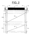
- the current sources 25 and 30 simultaneously charge up the capacitor 10, resulting in a ramp voltage at the output terminal 60 (the ramp 80 of FIG. 2).
- a synchronisation pulse 95 of the television signal provides timing for the start of each excursion of the ramp 80.
- the line decoder circuit (not shown) momentarily closes the switch 45 which discharges the ramp capacitor 10 through the resistor 40.
- the switch 45 is opened, the ramp capacitor 10 begins to charge and the ramp voltage increases.
- the ramp voltage produces a varying current in the connected vertical deflection circuit.
- the value of the ramp capacitor 10 and the current sources 25 and 30 are such that the variation in the ramp voltage is sufficient to enable the deflection coils of the vertical deflection circuit to fill the television screen with the wanted visible signal.
- Sampling lines 85 added by the television to the television signal occur just before the ramp voltage is large enough to provide sufficient current to the vertical deflection coils to place the signal in the visible part of the television screen. Therefore the sampling lines 85 of the 4:3 picture do not appear to the viewer because they are produced just above the visible part of the screen.
- a television signal having an aspect ratio of 16:9 is to be produced on the same 4:3 aspect television screen.
- the first switch 35 of the circuit 5 is set open, such that only the first current source 25 is connected to the terminal 15.
- the ratio of the current sources is arranged such that the first source 25 produces 75% of the current of the combined arrangement of two sources. In this way a reduced current charges up the ramp capacitor 10. Since the charge stored in a capacitor is proportional to the charging current supplied to it, the ramp 90 resulting from the charging of the capacitor 10 has only 75% of the vertical range of the ramp 80. Therefore the current supplied to the vertical deflection circuit is also only 75% of that required for a full height picture on the television screen.
- the third switch 55 is set closed, such that the input terminal 65 is coupled to the voltage adder circuit 50.
- the timing pulse (70 of FIG. 2) present at the input terminal 65 is decoded from the line counter of the television (not shown) by the line decoder circuit described above (not shown).
- the timing pulse 70 (zero voltage at the input terminal 65) is arranged to start just after the line 1 of the television signal (the synchronisation pulse 95) and finish after the last of the sampling lines 85 but before the first line of useful picture signal (the block 75).
- the timing pulse 70 is arranged to be active low, so at all other times there is a fixed voltage level at the input terminal 65.
- the voltage adder circuit adds the fixed voltage to the ramp voltage at the output terminal 60, except at the occurrence of the timing pulse 70, when the added voltage value is zero.
- the fixed voltage increases the ramp voltage by a constant amount. This vertically offsets the ramp 90, resulting in a downward shift of the generated picture.
- the fixed voltage level is appropriately chosen such that the offset is 12.5% of the full screen height. Hence the 16:9 picture appears in the centre of the screen.
- the sampling lines 85 are added to both the 16:9 and 4:3 television signals just after the synchronisation pulse 95.
- the line decoder circuit sets the switch 45 closed to discharge the capacitor 10 and therefore reset the ramp 90.
- the line decoder circuit is set to keep the switch 45 closed until after the sampling lines 85 have occurred. In this way the starting point (in time) of the ramp voltage is adjusted by holding it at zero until the sampling lines have been put on the screen.
- the timing pulse at the input terminal 65 ensures that the nominal supply voltage which generates the ramp offset is inhibited during this time. If this were not done, the supply voltage added to the ramp voltage would place the sampling lines in the visible screen area.
- the ramp 90 is held at zero for the duration of the sampling lines and hence the vertical deflection circuit holds the television signal at the top of the screen when the sampling lines occur.
- the 16:9 picture can be fully viewed on the 4:3 screen, and the sampling lines which are not desired in the visible area of the screen but which must not be blanked are held at the top of the screen, out of the visible area.
- a switched capacitor arrangement comprising a first capacitor and a second selectively coupled capacitor, charged by a single current source, could be used to provide the first and second ramp voltages instead of the capacitor 10 and the two current sources 25 and 30.
- timing pulse could be used to time and add the predetermined voltage, such as the synchronisation pulse used in conjunction with a delay arrangement.
- the circuit could be arranged to work with aspect ratios other than the two mentioned above, and for other types of unwanted lines added at other portions of the television signal.
Description
Claims (10)
- A television vertical timebase circuit comprising,means (10,25,30,35) for generating a vertical ramp voltage of selectively one of first (80) and second (90) slopes corresponding to respective first and second picture aspect ratios in which the second aspect ratio has a smaller picture height than the first, andmeans (50,55) for adding a predetermined voltage to a predetermined portion of the ramp voltage of the second slope to adjust the vertical starting position on the screen of pictures of the second aspect ratio by a downward shift, and means (45;55) for inhibiting adding the predetermined voltage during the occurrence of unwanted visible signals, ie signals which are not bound for display, such that said unwanted visible signals are positioned outside the visible screen area when displaying pictures of the second aspect ratio.
- The television vertical timebase circuit of claim 1 further comprising means (40,45) for inhibiting generation of the ramp voltage of the second slope during the occurrence of the unwanted visible signals.
- The television vertical timebase circuit of claim 1 or claim 2 wherein said means for generating comprises current source means (25,30) arranged to charge a capacitor (10).
- The television vertical timebase circuit of claim 2 or claim 3 wherein said means for inhibiting generation of the ramp voltage comprises means for inhibiting charging of the capacitor during the occurrence of the unwanted visible signals.
- The television vertical timebase circuit of claim 3 wherein said current source means comprises two current sources arranged to simultaneously charge the capacitor to provide one of the two ramp voltages and wherein one current source thereof is arranged to charge the capacitor to provide the other of the two ramp voltages.
- The television vertical timebase circuit of any preceding claim wherein the first and second picture aspect ratios are 4:3 and 16:9 respectively.
- The television vertical timebase circuit of any preceding claim wherein said predetermined portion of said ramp voltage of said second slope is that portion which coincides with the portion of the television picture which does not contain said unwanted visible signals.
- The television vertical timebase circuit of any preceding claim wherein said predetermined voltage is an offset voltage arranged to vertically offset the second television picture such that it is placed centrally on the screen.
- The television vertical timebase circuit of any preceding claim wherein said unwanted visible signals are sampling lines added to the television signal.
- The television vertical timebase circuit of any preceding claim wherein said adding means is a voltage adder circuit.
Applications Claiming Priority (3)
| Application Number | Priority Date | Filing Date | Title |
|---|---|---|---|
| GB9320340A GB2282513B (en) | 1994-10-06 | 1993-10-02 | Television vertical timebase circuit |
| GB9320340 | 1993-10-02 | ||
| US08/318,932 US5606228A (en) | 1993-10-02 | 1994-10-06 | Television vertical timebase circuit |
Publications (3)
| Publication Number | Publication Date |
|---|---|
| EP0647065A2 EP0647065A2 (en) | 1995-04-05 |
| EP0647065A3 EP0647065A3 (en) | 1995-07-19 |
| EP0647065B1 true EP0647065B1 (en) | 1998-12-02 |
Family
ID=26303622
Family Applications (1)
| Application Number | Title | Priority Date | Filing Date |
|---|---|---|---|
| EP94114579A Expired - Lifetime EP0647065B1 (en) | 1993-10-02 | 1994-09-15 | Generating vertical deflection signals for television |
Country Status (6)
| Country | Link |
|---|---|
| US (1) | US5606228A (en) |
| EP (1) | EP0647065B1 (en) |
| JP (1) | JPH07162809A (en) |
| CZ (1) | CZ284988B6 (en) |
| PL (1) | PL175181B1 (en) |
| SK (1) | SK280743B6 (en) |
Family Cites Families (12)
| Publication number | Priority date | Publication date | Assignee | Title |
|---|---|---|---|---|
| US4760455A (en) * | 1985-11-29 | 1988-07-26 | Canon Kabushiki Kaisha | Picture output device |
| GB8602644D0 (en) * | 1986-02-04 | 1986-03-12 | British Broadcasting Corp | Video systems |
| JPH02276368A (en) * | 1989-04-18 | 1990-11-13 | Sony Corp | Television receiver |
| DE3936584A1 (en) * | 1989-11-03 | 1991-05-08 | Thomson Brandt Gmbh | CIRCUIT FOR DARK RADIATION CURRENT CONTROL IN A TELEVISION RECEIVER |
| US5442406A (en) * | 1990-06-01 | 1995-08-15 | Thomson Consumer Electronics, Inc. | Wide screen television |
| US5414463A (en) * | 1991-09-18 | 1995-05-09 | Hitachi, Ltd. | Video cameras capable of switching an aspect ratio and view finders for use in the same |
| JPH0591357A (en) * | 1991-09-30 | 1993-04-09 | Sanyo Electric Co Ltd | Vertical deflection circuit |
| ES2108083T3 (en) * | 1991-10-16 | 1997-12-16 | Philips Electronics Nv | DEVICE FOR VISUALIZATION OF IMAGES IN FORMAT 16/9 ABLE TO RECEIVE IMAGES IN FORMAT 4/3. |
| DE4139403C2 (en) * | 1991-11-29 | 1994-02-17 | Sony Corp | Scan display device |
| GB2254977B (en) * | 1992-04-23 | 1996-01-17 | Philips Electronics Nv | Receiver for letterbox television signals |
| JP3326830B2 (en) * | 1992-11-17 | 2002-09-24 | ソニー株式会社 | Video equipment |
| US5359267A (en) * | 1993-09-03 | 1994-10-25 | Thomson Consumer Electronics, Inc. | Vertical deflection with vertical shrink mode |
-
1994
- 1994-09-15 EP EP94114579A patent/EP0647065B1/en not_active Expired - Lifetime
- 1994-09-28 JP JP6257288A patent/JPH07162809A/en active Pending
- 1994-09-30 SK SK1189-94A patent/SK280743B6/en unknown
- 1994-09-30 PL PL94305261A patent/PL175181B1/en unknown
- 1994-09-30 CZ CZ942403A patent/CZ284988B6/en not_active IP Right Cessation
- 1994-10-06 US US08/318,932 patent/US5606228A/en not_active Expired - Fee Related
Also Published As
| Publication number | Publication date |
|---|---|
| PL305261A1 (en) | 1995-04-03 |
| PL175181B1 (en) | 1998-11-30 |
| JPH07162809A (en) | 1995-06-23 |
| CZ284988B6 (en) | 1999-04-14 |
| CZ240394A3 (en) | 1995-05-17 |
| SK118994A3 (en) | 1995-06-07 |
| EP0647065A3 (en) | 1995-07-19 |
| EP0647065A2 (en) | 1995-04-05 |
| SK280743B6 (en) | 2000-07-11 |
| US5606228A (en) | 1997-02-25 |
Similar Documents
| Publication | Publication Date | Title |
|---|---|---|
| EP0630154B1 (en) | Television receiver capable of enlarging and compressing image | |
| US4412251A (en) | Flicker preventing circuit | |
| EP0136824B2 (en) | Automatic contrast reduction circuit for a teletext or monitor operation | |
| PL166499B1 (en) | Beam deflection speed modulation system | |
| US5486870A (en) | Apparatus for the display of pictures having an aspect ratio 4/3 on a display having an aspect ratio of 16/9 | |
| US5680176A (en) | Apparatus for controlling caption display on a wide aspect ratio | |
| US4660084A (en) | Television receiver with selectable video input signals | |
| JPH1188716A (en) | Display device | |
| US4660085A (en) | Television receiver responsive to plural video signals | |
| EP0647065B1 (en) | Generating vertical deflection signals for television | |
| US5177612A (en) | Signal switching output device | |
| GB2282513A (en) | Television vertical timebase circuit | |
| EP0136823B1 (en) | On-screen display system | |
| US4612574A (en) | Oscillator-frequency control interface circuit | |
| US5519445A (en) | Television receiver having caption displaying capability | |
| US3795767A (en) | High voltage protection circuit | |
| EP0498813B1 (en) | Circuit for the cut off regulation in a television receiver | |
| KR0119803Y1 (en) | Brightness control system of wide tv | |
| EP0508785B1 (en) | Scrolling superimposition of generated title | |
| KR100206589B1 (en) | Automatic image width control apparatus in case of letterbox input | |
| KR100486196B1 (en) | Television system without afterimage of auto kine bias reference signal and method for removing the after image thereof | |
| GB2253978A (en) | Raster scan system without flyback | |
| KR100263953B1 (en) | Apparatus for the display of pictures | |
| JPH0678328A (en) | Color television receiver | |
| JPH06165058A (en) | Crt |
Legal Events
| Date | Code | Title | Description |
|---|---|---|---|
| PUAI | Public reference made under article 153(3) epc to a published international application that has entered the european phase |
Free format text: ORIGINAL CODE: 0009012 |
|
| AK | Designated contracting states |
Kind code of ref document: A2 Designated state(s): DE ES FR IT |
|
| PUAL | Search report despatched |
Free format text: ORIGINAL CODE: 0009013 |
|
| AK | Designated contracting states |
Kind code of ref document: A3 Designated state(s): DE ES FR IT |
|
| 17P | Request for examination filed |
Effective date: 19960119 |
|
| GRAG | Despatch of communication of intention to grant |
Free format text: ORIGINAL CODE: EPIDOS AGRA |
|
| 17Q | First examination report despatched |
Effective date: 19971209 |
|
| GRAG | Despatch of communication of intention to grant |
Free format text: ORIGINAL CODE: EPIDOS AGRA |
|
| GRAG | Despatch of communication of intention to grant |
Free format text: ORIGINAL CODE: EPIDOS AGRA |
|
| GRAH | Despatch of communication of intention to grant a patent |
Free format text: ORIGINAL CODE: EPIDOS IGRA |
|
| GRAH | Despatch of communication of intention to grant a patent |
Free format text: ORIGINAL CODE: EPIDOS IGRA |
|
| GRAA | (expected) grant |
Free format text: ORIGINAL CODE: 0009210 |
|
| AK | Designated contracting states |
Kind code of ref document: B1 Designated state(s): DE ES FR IT |
|
| PG25 | Lapsed in a contracting state [announced via postgrant information from national office to epo] |
Ref country code: ES Free format text: THE PATENT HAS BEEN ANNULLED BY A DECISION OF A NATIONAL AUTHORITY Effective date: 19981202 |
|
| REF | Corresponds to: |
Ref document number: 69414967 Country of ref document: DE Date of ref document: 19990114 |
|
| ET | Fr: translation filed | ||
| PLBE | No opposition filed within time limit |
Free format text: ORIGINAL CODE: 0009261 |
|
| STAA | Information on the status of an ep patent application or granted ep patent |
Free format text: STATUS: NO OPPOSITION FILED WITHIN TIME LIMIT |
|
| 26N | No opposition filed | ||
| PGFP | Annual fee paid to national office [announced via postgrant information from national office to epo] |
Ref country code: FR Payment date: 20010831 Year of fee payment: 8 |
|
| REG | Reference to a national code |
Ref country code: FR Ref legal event code: D6 |
|
| PGFP | Annual fee paid to national office [announced via postgrant information from national office to epo] |
Ref country code: DE Payment date: 20010927 Year of fee payment: 8 |
|
| PG25 | Lapsed in a contracting state [announced via postgrant information from national office to epo] |
Ref country code: DE Free format text: LAPSE BECAUSE OF NON-PAYMENT OF DUE FEES Effective date: 20030401 |
|
| PG25 | Lapsed in a contracting state [announced via postgrant information from national office to epo] |
Ref country code: FR Free format text: LAPSE BECAUSE OF NON-PAYMENT OF DUE FEES Effective date: 20030603 |
|
| REG | Reference to a national code |
Ref country code: FR Ref legal event code: ST |
|
| PG25 | Lapsed in a contracting state [announced via postgrant information from national office to epo] |
Ref country code: IT Free format text: LAPSE BECAUSE OF NON-PAYMENT OF DUE FEES;WARNING: LAPSES OF ITALIAN PATENTS WITH EFFECTIVE DATE BEFORE 2007 MAY HAVE OCCURRED AT ANY TIME BEFORE 2007. THE CORRECT EFFECTIVE DATE MAY BE DIFFERENT FROM THE ONE RECORDED. Effective date: 20050915 |