EP0645002B1 - Thermal isolation microstructure - Google Patents
Thermal isolation microstructure Download PDFInfo
- Publication number
- EP0645002B1 EP0645002B1 EP92914472A EP92914472A EP0645002B1 EP 0645002 B1 EP0645002 B1 EP 0645002B1 EP 92914472 A EP92914472 A EP 92914472A EP 92914472 A EP92914472 A EP 92914472A EP 0645002 B1 EP0645002 B1 EP 0645002B1
- Authority
- EP
- European Patent Office
- Prior art keywords
- silicon nitride
- layer
- thin film
- depositing
- legs
- Prior art date
- Legal status (The legal status is an assumption and is not a legal conclusion. Google has not performed a legal analysis and makes no representation as to the accuracy of the status listed.)
- Expired - Lifetime
Links
Images


Classifications
-
- G—PHYSICS
- G01—MEASURING; TESTING
- G01J—MEASUREMENT OF INTENSITY, VELOCITY, SPECTRAL CONTENT, POLARISATION, PHASE OR PULSE CHARACTERISTICS OF INFRARED, VISIBLE OR ULTRAVIOLET LIGHT; COLORIMETRY; RADIATION PYROMETRY
- G01J5/00—Radiation pyrometry, e.g. infrared or optical thermometry
- G01J5/10—Radiation pyrometry, e.g. infrared or optical thermometry using electric radiation detectors
- G01J5/20—Radiation pyrometry, e.g. infrared or optical thermometry using electric radiation detectors using resistors, thermistors or semiconductors sensitive to radiation, e.g. photoconductive devices
Definitions
- the invention relates to the field of microstructure infrared radiation detector elements.
- Good thermal isolation of infrared radiation detector elements is required to maximise performance.
- the thermal isolation provided by the long detector support legs is presently limited because the relatively long legs must be thick enough to not break during turbulent liquid anisotropic etch of the pit in the silicon substrate beneath the detector, as well as thick enough to maintain the detector suspended out of contact with the substrate during and after the anisotropic etch.
- the present invention provides a process for fabricating a thermal isolation microbridge used as an infrared radiation detection element, the steps comprising: providing a monocrystalline silicon substrate wafer having a planar surface; depositing a thin film silicon nitride layer on said surface; depositing and delineating a thin film layer of temperature-sensitive, electrically-resistive material for a sensor and electrode leadout on said silicon nitride layer; depositing a further thin film silicon nitride layer over said material and said first silicon nitride layer; depositing a thin absorber layer over the last deposited silicon nitride in the area of the sensor; depositing and delineating a thin film photo-lithographic mask; making a plurality of silicon nitride cuts outlining elongated legs containing the electrode leadout and the support tabs for the microbridge; dry etching the legs and the support tabs to remove about 1/2 the thickness of silicon nitride; introducing anisotropic etchant through said cuts and anis
- Figure 1 shows a plan view of the microbridge infrared radiation detector element according to the invention.
- Figure 1a shows a cross section of the completed support leg for the microbridge element.
- Figure 2 shows an edge view of the structure Figure 1.
- Figure 3 shows the plan view at an intermediate point in the process before tab removal, and before the support legs are made narrower and thinner by the final dry etch. Metal lines are not shown.
- Figure 3a shows a cross section of the support leg prior to the thinning steps.
- Figure 4a and 4b are cross section of the support leg prior to the thinning steps.
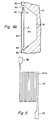
- Figures 4a and 4b are cross section views of Figure 3.
- Figure 5 shows and exemplary sensing element embedded in the microbridge.
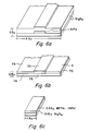
- Figures 6a, b, and c show successive steps in the process of fabricating the support legs.
- a single crystalline (100) silicon substrate 11 has grown on the surface thereof a thin film layer of dielectric 12, 13 such as silicon nitride (Si 3 N 4 ).
- dielectric 12, 13 such as silicon nitride (Si 3 N 4 ).
- a thin film resistive radiation sensing element 14 is embedded in the silicon nitride, a thin film IR absorber layer 16 is over the dielectric; a pit 15 is etched out of the silicon beneath the sensing element, and the silicon nitride 12, 13 with sensing element 14 and absorber 16 is a thermally isolated bridge 17 over the etched pit in silicon substrate.
- the microbridge 17 is supported by two long thin support legs 20 and 21.
- the objective of the invention is to decrease the thermal conductance of the detector support leg by fabricating a leg having a cross section shown in Figure la which contrasts to the earlier designed cross section shown in Figure 3a.
- the thermal conductance of the Figure 1a leg is due to the conductance of the metal electrode combined with that of the nitride.
- the conductance can be one half or less that of the conductance of the leg shown in Figure 3a, depending on the electrode metal that is used.
- a conventional metal is 80Ni;20Fe alloy. Other conductive metals could be used.
- the leg of Figure 1a is too weak to withstand the turbulent etch process during which liquid forces on the detector could break such thin support legs.
- This difficulty can be avoided by designing the support legs with connecting tabs as shown in Figure 3.
- the legs and their support tabs are then thinned to about 1/2 thickness before the liquid anisotropic etch.
- the main detector area is protected during this step by a chrome metal mask which extends a few microns beyond the absorber layer and the pit side wall as shown in Figure 3.
- the tabs also prevent the collapse of the detector into the etch pit. This potential collapse into the pit would occur because of surface tension effects.
- the chrome mask is removed by a final liquid etch.
- a final plasma "dry” etch then thins the legs and removes the support tabs by removing the last approximately 1.5 ⁇ 10 -7 m (1500 angstroms) of nitride, leaving the leg cross section of Figure 1a.
- the absorber layer over the main detector acts as an etch stop.
- a length of metal electrode a few ⁇ m long in the leg will still be encased in nitride at each end of the leg a a precaution against electrical leakage and shorting to the absorber layer 16 or the silicon substrate.
- the tabs will have been eliminated, and the long narrow electrode/nitride bimorph will tend to bend upward to raise the main detector 17 safely above the substrate, that is, to give a positive elevation of the detector above the substrate to prevent thermal shorting.
- FIG. 1 there is shown the top plan view of a microbridge infrared radiation detector element 10.
- Figure 2 is an edge view or sectional view of Figure 1 and carries like identifying numerals.
- the sensing element is made up of a sensing area identified by dashed lines.
- the sensing area or radiation sensing means could be a thin film sinuous nickel-iron resistor element or an area of deposited thin film of some other temperature-sensitive electrically resistive material.
- the substrate 11 is single crystalline (100) silicon having a planar surface 11a upon which has been sputter deposited a thin film layer 12, 13 of a dielectric such as silicon nitride.
- the thin film layer may be on the order of a ⁇ m in thickness and may have about half of the layer deposited first, then a thin film resistive layer 14, such as NiFe, is sputtered on and delineated, followed by the depositing of the remainder 13 of the nitride layer to embed the resistive layer.
- the thickness of the NiFe layer 14 is about 8 ⁇ 10 -8 (800 angstroms).
- the delineating of the resistive layer 14 is to provide a sinuous (see Figure 5) or tortuous resistive path 14' through the sensing area 17 starting at an entrance point 22 and continuing to an exit point 23.
- the sinuous path shown in the sensing area 17 is exemplary for obtaining a desired resistance value and is not a part of the invention.
- the radiation sensing means has a pair of elongated support legs including leadout means which provide the electrical connections to and from the radiation sensing means.
- the leadout means are fabricated on a pair of silicon nitride leadout areas between two etch window cuts in the silicon nitride and semienclose the sensing means.
- the window cuts in the silicon nitride are areas defined for providing access to introduce anisotropic etchant for anisotropically etching a pit beneath the sensing area.
- the L-shaped support leg 20 is connected to the bridge member 17 at tab 30 and to the substrate at the opposite end 31.
- the L-shaped support leg 21 is connected in supporting relation to the bridge member 17 at tab 32 and to the substrate at the opposite end 33.
- FIG. la An enlarged cross sectional view of the completed L-shaped support legs 20 and 21 is shown in Figure la and comprises the NiFe conductor 35 (i.e., layer 14) on the nitride strip 36 (i.e., layer 12).
- Exemplary dimensions of the support legs are shown in Figure 1a with a width of 1.5 ⁇ m, a nitride thickness of 1 ⁇ 10 -7 m(.10 micron) and a 4 ⁇ 10 -8 m (.04 micron) metal thickness. Since the leg 20 (or 21) extends around two adjacent sides of the perimeter of the microbridge, the length of the L-shaped support leg is on the order of 6 ⁇ 10 -4 m (600 microns).
- the L-shaped legs 20 and 21 are bordered by a pair of interlocking cuts 40 and 50 through the silicon nitride layer 12, 13.
- these silicon nitride cuts are six sections in number and sections are separated by leg supporting tabs.
- FIG. 3 (which is in many ways similar to Figure 1) there is shown the top plan view at an intermediate point in the process of fabricating the sensor structure and before all the steps are completed that result in the final device.
- one set of the silicon nitride cuts 41, 42, 43 and 44 is shown which in the final device is numbered 40.
- Another set of silicon nitride cuts 51, 52, 53 and 54 is shown which in the final device is numbered 50.
- Between adjacent ends of cuts 41 and 42 is a tab 45; adjacent ends of cuts 42 and 43 is a tab 46, and between adjacent ends of cuts 53 and 54 is a tab 55; between adjacent ends of cuts 52 and 53 is a tab 56; and between adjacent ends of cuts 53 and 54 is a tab 57.
- the six tabs are positioned along the length of the legs to stabilize and protect the legs and main detector area until the turbulent liquid etch process is completed. Without the protection of the tabs there would be the possibility of a collapse of the detector into the etch pit which could occur because of surface tension effects.
- the six tabs are to be removed in final stages of fabrication.
- Figure 4a is a cross section view taken at line 4a 4a of Figure 3.
- the layer structure is predominantly the same as explained in Figure 2.
- an additional thin film chromium photolithographic metal mask 60 is shown which has been deposited and delineated over the structure to protect it while a dry etch step thins the uncoated Si 3 N 4 of the legs 20' and 21' and their six support tabs.
- Figure 6a shows a short section of the leg 20' (or 21') prior to the dry etch. At that point the legs are about 3.5 ⁇ m wide and about 0.3 ⁇ m in thickness. Following the dry etch step which removes about half of the silicon nitride the structure appears as shown in Figure 6B.
- FIG. 3 The six thinned support tabs are still intact, Figure 3, to support the legs and sensor structure during the anisotropic etch.
- Figure 4a is shown the thinned legs 20' and 21' as well as tab 45 as also shown is the etched pit following the anisotropic etch.
- Figure 3 the hatched area is added to represent the plan view location of the temporary chrome mask 50.
- Figure 4b is shown a section from the other direction.
- Figure 4b there is shown the thinned leg 21' and the thinned tab 47. Slots 43 and 52 are shown.
- FIG. 1 there is shown a sensing area 17.
- the NiFe sensor is shown at layer 14 of Figure 2.
- Figure 5 shows in more detail how the embedded sensor 14 layout and electrode leadout would preferably be designed.
Landscapes
- Physics & Mathematics (AREA)
- General Physics & Mathematics (AREA)
- Spectroscopy & Molecular Physics (AREA)
- Photometry And Measurement Of Optical Pulse Characteristics (AREA)
- Radiation Pyrometers (AREA)
- Semiconductor Integrated Circuits (AREA)
- Element Separation (AREA)
Abstract
Description
- The US Government has certain rights in this invention pursuant to the terms of a Contract DAAL01-85-C-0153.
- The invention relates to the field of microstructure infrared radiation detector elements. Good thermal isolation of infrared radiation detector elements is required to maximise performance. The thermal isolation provided by the long detector support legs is presently limited because the relatively long legs must be thick enough to not break during turbulent liquid anisotropic etch of the pit in the silicon substrate beneath the detector, as well as thick enough to maintain the detector suspended out of contact with the substrate during and after the anisotropic etch.
- The present invention provides a process for fabricating a thermal isolation microbridge used as an infrared radiation detection element, the steps comprising: providing a monocrystalline silicon substrate wafer having a planar surface; depositing a thin film silicon nitride layer on said surface; depositing and delineating a thin film layer of temperature-sensitive, electrically-resistive material for a sensor and electrode leadout on said silicon nitride layer; depositing a further thin film silicon nitride layer over said material and said first silicon nitride layer; depositing a thin absorber layer over the last deposited silicon nitride in the area of the sensor; depositing and delineating a thin film photo-lithographic mask; making a plurality of silicon nitride cuts outlining elongated legs containing the electrode leadout and the support tabs for the microbridge; dry etching the legs and the support tabs to remove about 1/2 the thickness of silicon nitride; introducing anisotropic etchant through said cuts and anisotropically etching away silicon to form a pit beneath the microbridge sensor legs; removing the thin film photolithographic mask with a liquid etch; etching with a plasma dry etch the exposed silicon nitride on said elongated legs to remove the Si3N4 of the leg extending laterally of the electrode so as to remove the support tabs.
- Figure 1 shows a plan view of the microbridge infrared radiation detector element according to the invention.
- Figure 1a shows a cross section of the completed support leg for the microbridge element.
- Figure 2 shows an edge view of the structure Figure 1.
- Figure 3 shows the plan view at an intermediate point in the process before tab removal, and before the support legs are made narrower and thinner by the final dry etch. Metal lines are not shown.
- Figure 3a shows a cross section of the support leg prior to the thinning steps.
- Figure 4a and 4b are cross section of the support leg prior to the thinning steps.
- Figures 4a and 4b are cross section views of Figure 3.
- Figure 5 shows and exemplary sensing element embedded in the microbridge.
- Figures 6a, b, and c show successive steps in the process of fabricating the support legs.
- Broadly stated, in the construction of a microbridge sensor device 10 a single crystalline (100) silicon substrate 11 has grown on the surface thereof a thin film layer of dielectric 12, 13 such as silicon nitride (Si3N4). Generally speaking, a thin film resistive
radiation sensing element 14 is embedded in the silicon nitride, a thin filmIR absorber layer 16 is over the dielectric; apit 15 is etched out of the silicon beneath the sensing element, and thesilicon nitride sensing element 14 and absorber 16 is a thermally isolatedbridge 17 over the etched pit in silicon substrate. Themicrobridge 17 is supported by two longthin support legs - The objective of the invention is to decrease the thermal conductance of the detector support leg by fabricating a leg having a cross section shown in Figure la which contrasts to the earlier designed cross section shown in Figure 3a. The thermal conductance of the Figure 1a leg is due to the conductance of the metal electrode combined with that of the nitride. The conductance can be one half or less that of the conductance of the leg shown in Figure 3a, depending on the electrode metal that is used. A conventional metal is 80Ni;20Fe alloy. Other conductive metals could be used.
- The leg of Figure 1a is too weak to withstand the turbulent etch process during which liquid forces on the detector could break such thin support legs. This difficulty can be avoided by designing the support legs with connecting tabs as shown in Figure 3. The legs and their support tabs are then thinned to about 1/2 thickness before the liquid anisotropic etch. The main detector area is protected during this step by a chrome metal mask which extends a few microns beyond the absorber layer and the pit side wall as shown in Figure 3. During the anisotropic etch, the tabs also prevent the collapse of the detector into the etch pit. This potential collapse into the pit would occur because of surface tension effects. After the anisotropic etch, the chrome mask is removed by a final liquid etch. A final plasma "dry" etch then thins the legs and removes the support tabs by removing the last approximately 1.5×10⁻⁷m (1500 angstroms) of nitride, leaving the leg cross section of Figure 1a.
- During the last plasma dry etch, the absorber layer over the main detector acts as an etch stop. When completed, a length of metal electrode a few µm long in the leg will still be encased in nitride at each end of the leg a a precaution against electrical leakage and shorting to the
absorber layer 16 or the silicon substrate. When the last plasma dry etch is finished, the tabs will have been eliminated, and the long narrow electrode/nitride bimorph will tend to bend upward to raise themain detector 17 safely above the substrate, that is, to give a positive elevation of the detector above the substrate to prevent thermal shorting. - Referring now to Figure 1 there is shown the top plan view of a microbridge infrared
radiation detector element 10. Figure 2 is an edge view or sectional view of Figure 1 and carries like identifying numerals. The sensing element is made up of a sensing area identified by dashed lines. The sensing area or radiation sensing means could be a thin film sinuous nickel-iron resistor element or an area of deposited thin film of some other temperature-sensitive electrically resistive material. In these figures can be seen a completed detector element structure. The substrate 11 is single crystalline (100) silicon having a planar surface 11a upon which has been sputter deposited athin film layer resistive layer 14, such as NiFe, is sputtered on and delineated, followed by the depositing of theremainder 13 of the nitride layer to embed the resistive layer. The thickness of theNiFe layer 14 is about 8×10⁻⁸ (800 angstroms). The delineating of theresistive layer 14 is to provide a sinuous (see Figure 5) or tortuous resistive path 14' through thesensing area 17 starting at anentrance point 22 and continuing to anexit point 23. The sinuous path shown in thesensing area 17 is exemplary for obtaining a desired resistance value and is not a part of the invention. - The radiation sensing means has a pair of elongated support legs including leadout means which provide the electrical connections to and from the radiation sensing means. The leadout means are fabricated on a pair of silicon nitride leadout areas between two etch window cuts in the silicon nitride and semienclose the sensing means. The window cuts in the silicon nitride are areas defined for providing access to introduce anisotropic etchant for anisotropically etching a pit beneath the sensing area. The L-
shaped support leg 20 is connected to thebridge member 17 attab 30 and to the substrate at theopposite end 31. Likewise, the L-shaped support leg 21 is connected in supporting relation to thebridge member 17 attab 32 and to the substrate at the opposite end 33. An enlarged cross sectional view of the completed L-shaped support legs shaped legs interlocking cuts silicon nitride layer - Referring now to Figure 3 (which is in many ways similar to Figure 1) there is shown the top plan view at an intermediate point in the process of fabricating the sensor structure and before all the steps are completed that result in the final device. In Figure 3 one set of the
silicon nitride cuts cuts tab 45; adjacent ends ofcuts tab 46, and between adjacent ends ofcuts tab 55; between adjacent ends ofcuts tab 56; and between adjacent ends ofcuts tab 57. The six tabs are positioned along the length of the legs to stabilize and protect the legs and main detector area until the turbulent liquid etch process is completed. Without the protection of the tabs there would be the possibility of a collapse of the detector into the etch pit which could occur because of surface tension effects. The six tabs are to be removed in final stages of fabrication. - Figure 4a is a cross section view taken at line 4a 4a of Figure 3. In this figure the layer structure is predominantly the same as explained in Figure 2. In this intermediate stage an additional thin film chromium
photolithographic metal mask 60 is shown which has been deposited and delineated over the structure to protect it while a dry etch step thins the uncoated Si3N4 of thelegs 20' and 21' and their six support tabs. Figure 6a shows a short section of theleg 20' (or 21') prior to the dry etch. At that point the legs are about 3.5µm wide and about 0.3µm in thickness. Following the dry etch step which removes about half of the silicon nitride the structure appears as shown in Figure 6B. The six thinned support tabs are still intact, Figure 3, to support the legs and sensor structure during the anisotropic etch. In Figure 4a is shown the thinnedlegs 20' and 21' as well astab 45 as also shown is the etched pit following the anisotropic etch. In Figure 3 the hatched area is added to represent the plan view location of thetemporary chrome mask 50. In Figure 4b is shown a section from the other direction. In Figure 4b there is shown the thinned leg 21' and the thinnedtab 47.Slots - After the pit has been etched anisotropically the turbulent etch procedures are completed. The
protective chrome 60 has now served its purpose and is removed with a final liquid etch. Referring now to the legs shown in Figure 6c as compared with Figure 6b, a final plasma etch removes the remainingsilicon nitride 70 over the metal conductor and also thesilicon nitride areas silicon nitride 75 under the metal conductor is protected by the metal and remains as shown in Figure 6c. As the Si3N4 is etched away to release the tabs there is a bimorph affect of the remaining portion of the legs to tend to raise themain detector 17 and keep it above the substrate preserving the thermal isolation under the detector. - Referring again to Figure 1 there is shown a
sensing area 17. The NiFe sensor is shown atlayer 14 of Figure 2. Figure 5 shows in more detail how the embeddedsensor 14 layout and electrode leadout would preferably be designed. -
- 1. Provide monocrystalline silicon wafer substrate.
- 2. Deposit Si3N4 layer.
- 3. Deposit and delineate NiFe sensor and leads.
- 4. Deposit Si3N4 layer to embed NiFe in the Si3N4.
- 5. Deposit absorber layer of NiFe.
- 6. Cover absorber layer with 30-40 nm Si3N4.
- 7. Cover surface with chrome metal mask and delineate chrome.
- 8. Make six Si3N4 etch cuts.
- 9. Thin legs and support tabs to 1/2 thickness by dry etch.
- 10. Anisotropically etch the pit in Si.
- 11. Remove chrome with final liquid etch.
- 12. Perform final plasma dry etch to thin and narrow legs and remove support tabs by removing Si3N4.
Claims (6)
- A process for fabricating a thermal isolation microbridge used as an infrared radiation detection element, the steps comprising:providing a monocrystalline silicon substrate wafer (11) having a planar surface;depositing a thin film silicon nitride layer (12) on said surface;depositing and delineating a thin film layer (14) of temperature-sensitive, electrically-resistive material for a sensor and electrode leadout on said silicon nitride layer;depositing a further thin film silicon nitride layer (13) over said material and said silicon nitride layer;depositing a thin absorber layer (16) over the last deposited silicon nitride in the area of the sensor;depositing and delineating a thin film photo-lithographic mask (60),making a plurality of silicon nitride cuts (40, 50) outlining elongated legs (20, 21) containing the electrode leadout and the support tabs for the microbridge;dry etching the legs and the support tabs to remove about 1/2 the thickness of silicon nitride;introducing anisotropic etchant through said cuts and anisotropically etching away silicon to form a pit beneath the microbridge sensor legs;removing the thin film photolithographic mask with a liquid etch;etching with a plasma dry etch the exposed silicon nitride on said elongated legs to remove the Si3N4 of the leg extending laterally of the electrode so as to remove the support tabs.
- A process according to Claim 1 and directly following said step "depositing a thin absorber layer over the last deposited silicon nitride in the area of the sensor", further comprising the step:
covering said absorber layer with a thin film layer of silicon nitride. - A process according to Claim 1 or 2 in which said temperature sensitive electrically-resistive material is nickel-iron.
- A process according to any preceding Claim in which said absorber layer is a thin film layer of nickel-iron.
- A process according to any preceding Claim in which said photolithographic mask is chrome metal.
- A process according to any preceding Claim comprising etching with a plasma dry etch the exposed silicon nitride on said elongated legs to remove the Si3N4 down to the NiFe leadout, which NiFe acts as an etch stop to the dry etch, the plasma dry etch also removing the Si3N4 of the leg extending laterally of the electrode.
Applications Claiming Priority (1)
| Application Number | Priority Date | Filing Date | Title |
|---|---|---|---|
| PCT/US1992/005010 WO1993025878A1 (en) | 1992-06-11 | 1992-06-11 | Thermal isolation microstructure |
Publications (2)
| Publication Number | Publication Date |
|---|---|
| EP0645002A1 EP0645002A1 (en) | 1995-03-29 |
| EP0645002B1 true EP0645002B1 (en) | 1997-04-02 |
Family
ID=1242517
Family Applications (1)
| Application Number | Title | Priority Date | Filing Date |
|---|---|---|---|
| EP92914472A Expired - Lifetime EP0645002B1 (en) | 1992-06-11 | 1992-06-11 | Thermal isolation microstructure |
Country Status (5)
| Country | Link |
|---|---|
| EP (1) | EP0645002B1 (en) |
| JP (1) | JP2739610B2 (en) |
| CA (1) | CA2116678C (en) |
| DE (1) | DE69218796T2 (en) |
| WO (1) | WO1993025878A1 (en) |
Families Citing this family (9)
| Publication number | Priority date | Publication date | Assignee | Title |
|---|---|---|---|---|
| JP3374498B2 (en) | 1993-12-27 | 2003-02-04 | 株式会社デンソー | Infrared sensor |
| JP3287173B2 (en) * | 1995-04-07 | 2002-05-27 | 三菱電機株式会社 | Infrared detector |
| US5627112A (en) * | 1995-11-13 | 1997-05-06 | Rockwell International Corporation | Method of making suspended microstructures |
| JP3637665B2 (en) * | 1996-01-23 | 2005-04-13 | 松下電器産業株式会社 | Pyroelectric infrared detector |
| FR2752299B1 (en) * | 1996-08-08 | 1998-09-11 | Commissariat Energie Atomique | INFRARED DETECTOR AND MANUFACTURING METHOD THEREOF |
| JP3529596B2 (en) * | 1997-08-06 | 2004-05-24 | 株式会社東芝 | Infrared solid-state imaging device and method of manufacturing the same |
| JP3672516B2 (en) * | 2001-09-28 | 2005-07-20 | 株式会社東芝 | Infrared sensor device and manufacturing method thereof |
| WO2008073261A2 (en) * | 2006-12-08 | 2008-06-19 | Regents Of The University Of Minnesota | Detection beyond the standard radiation noise limit using reduced emissivity and optical cavity coupling |
| CN115950536B (en) * | 2023-01-12 | 2025-10-28 | 中国科学院上海技术物理研究所 | Electrostatically tuned filter based on arc-shaped cantilever microbridge process and its preparation method |
Family Cites Families (2)
| Publication number | Priority date | Publication date | Assignee | Title |
|---|---|---|---|---|
| AU631734B2 (en) * | 1990-04-18 | 1992-12-03 | Terumo Kabushiki Kaisha | Infrared ray sensor and method of manufacturing the same |
| WO1991016607A1 (en) * | 1990-04-26 | 1991-10-31 | Commonwealth Of Australia, The Secretary Department Of Defence | Semiconductor film bolometer thermal infrared detector |
-
1992
- 1992-06-11 JP JP6501420A patent/JP2739610B2/en not_active Expired - Lifetime
- 1992-06-11 CA CA002116678A patent/CA2116678C/en not_active Expired - Lifetime
- 1992-06-11 DE DE69218796T patent/DE69218796T2/en not_active Expired - Lifetime
- 1992-06-11 WO PCT/US1992/005010 patent/WO1993025878A1/en not_active Ceased
- 1992-06-11 EP EP92914472A patent/EP0645002B1/en not_active Expired - Lifetime
Also Published As
| Publication number | Publication date |
|---|---|
| JP2739610B2 (en) | 1998-04-15 |
| EP0645002A1 (en) | 1995-03-29 |
| DE69218796D1 (en) | 1997-05-07 |
| DE69218796T2 (en) | 1997-10-16 |
| CA2116678A1 (en) | 1993-12-23 |
| WO1993025878A1 (en) | 1993-12-23 |
| JPH07508095A (en) | 1995-09-07 |
| CA2116678C (en) | 2000-12-05 |
Similar Documents
| Publication | Publication Date | Title |
|---|---|---|
| US5534111A (en) | Thermal isolation microstructure | |
| US4784721A (en) | Integrated thin-film diaphragm; backside etch | |
| US4914742A (en) | Thin film orthogonal microsensor for air flow and method | |
| US4198744A (en) | Process for fabrication of fuse and interconnects | |
| KR100870039B1 (en) | Sensor for non-contact temperature measurement | |
| US6130109A (en) | Microbridge structure and method for forming a microstructure suspended by a micro support | |
| US4272753A (en) | Integrated circuit fuse | |
| EP0762510B1 (en) | Method for fabricating a monolithic semiconductor device with integrated surface micromachined structures | |
| JP3112680B2 (en) | Semiconductor film bolometer thermal infrared detector | |
| US5667879A (en) | TaN/NiFe/TaN anisotropic magnetic sensor element | |
| CA2116678C (en) | Thermal isolation microstructure | |
| JP5069241B2 (en) | Passivation structure for ferroelectric thin film devices. | |
| US4895616A (en) | Method for making thin film orthogonal microsensor for air flow | |
| US5753565A (en) | Method of reducing overetch during the formation of a semiconductor device | |
| US5310610A (en) | Silicon micro sensor and manufacturing method therefor | |
| US6828171B2 (en) | Systems and methods for thermal isolation of a silicon structure | |
| JPS6123503B2 (en) | ||
| EP0341964B1 (en) | Silicon micro sensor and manufacturing method therefor | |
| JP3534269B2 (en) | Semiconductor device and manufacturing method thereof | |
| CN1177203C (en) | Infrared bolometer | |
| JP3249174B2 (en) | Infrared sensor and method of manufacturing the same | |
| US6162696A (en) | Method of fabricating a feature in an integrated circuit using a two mask process with a single edge definition layer | |
| US6153501A (en) | Method of reducing overetch during the formation of a semiconductor device | |
| KR0161774B1 (en) | Semiconductor device and manufacturing method | |
| JPH10221143A (en) | Micro heater |
Legal Events
| Date | Code | Title | Description |
|---|---|---|---|
| PUAI | Public reference made under article 153(3) epc to a published international application that has entered the european phase |
Free format text: ORIGINAL CODE: 0009012 |
|
| 17P | Request for examination filed |
Effective date: 19941219 |
|
| AK | Designated contracting states |
Kind code of ref document: A1 Designated state(s): DE FR GB NL |
|
| 17Q | First examination report despatched |
Effective date: 19950614 |
|
| GRAG | Despatch of communication of intention to grant |
Free format text: ORIGINAL CODE: EPIDOS AGRA |
|
| GRAH | Despatch of communication of intention to grant a patent |
Free format text: ORIGINAL CODE: EPIDOS IGRA |
|
| GRAH | Despatch of communication of intention to grant a patent |
Free format text: ORIGINAL CODE: EPIDOS IGRA |
|
| GRAA | (expected) grant |
Free format text: ORIGINAL CODE: 0009210 |
|
| ITF | It: translation for a ep patent filed | ||
| AK | Designated contracting states |
Kind code of ref document: B1 Designated state(s): DE FR GB NL |
|
| REF | Corresponds to: |
Ref document number: 69218796 Country of ref document: DE Date of ref document: 19970507 |
|
| ET | Fr: translation filed | ||
| PLBE | No opposition filed within time limit |
Free format text: ORIGINAL CODE: 0009261 |
|
| STAA | Information on the status of an ep patent application or granted ep patent |
Free format text: STATUS: NO OPPOSITION FILED WITHIN TIME LIMIT |
|
| 26N | No opposition filed | ||
| REG | Reference to a national code |
Ref country code: GB Ref legal event code: IF02 |
|
| PGFP | Annual fee paid to national office [announced via postgrant information from national office to epo] |
Ref country code: FR Payment date: 20110603 Year of fee payment: 20 |
|
| PGFP | Annual fee paid to national office [announced via postgrant information from national office to epo] |
Ref country code: NL Payment date: 20110615 Year of fee payment: 20 Ref country code: GB Payment date: 20110523 Year of fee payment: 20 |
|
| PGFP | Annual fee paid to national office [announced via postgrant information from national office to epo] |
Ref country code: DE Payment date: 20110630 Year of fee payment: 20 |
|
| REG | Reference to a national code |
Ref country code: DE Ref legal event code: R071 Ref document number: 69218796 Country of ref document: DE |
|
| REG | Reference to a national code |
Ref country code: DE Ref legal event code: R071 Ref document number: 69218796 Country of ref document: DE |
|
| REG | Reference to a national code |
Ref country code: NL Ref legal event code: V4 Effective date: 20120611 |
|
| REG | Reference to a national code |
Ref country code: GB Ref legal event code: PE20 Expiry date: 20120610 |
|
| PG25 | Lapsed in a contracting state [announced via postgrant information from national office to epo] |
Ref country code: DE Free format text: LAPSE BECAUSE OF EXPIRATION OF PROTECTION Effective date: 20120612 |
|
| PG25 | Lapsed in a contracting state [announced via postgrant information from national office to epo] |
Ref country code: GB Free format text: LAPSE BECAUSE OF EXPIRATION OF PROTECTION Effective date: 20120610 |