EP0641091B1 - Apparatus using decision directed channel estimation in a digital mobile radio link - Google Patents
Apparatus using decision directed channel estimation in a digital mobile radio link Download PDFInfo
- Publication number
- EP0641091B1 EP0641091B1 EP94110653A EP94110653A EP0641091B1 EP 0641091 B1 EP0641091 B1 EP 0641091B1 EP 94110653 A EP94110653 A EP 94110653A EP 94110653 A EP94110653 A EP 94110653A EP 0641091 B1 EP0641091 B1 EP 0641091B1
- Authority
- EP
- European Patent Office
- Prior art keywords
- output
- adder
- signal
- multiplying
- input
- Prior art date
- Legal status (The legal status is an assumption and is not a legal conclusion. Google has not performed a legal analysis and makes no representation as to the accuracy of the status listed.)
- Expired - Lifetime
Links
Images


Classifications
-
- H—ELECTRICITY
- H04—ELECTRIC COMMUNICATION TECHNIQUE
- H04B—TRANSMISSION
- H04B1/00—Details of transmission systems, not covered by a single one of groups H04B3/00 - H04B13/00; Details of transmission systems not characterised by the medium used for transmission
- H04B1/69—Spread spectrum techniques
- H04B1/707—Spread spectrum techniques using direct sequence modulation
- H04B1/7097—Interference-related aspects
- H04B1/711—Interference-related aspects the interference being multi-path interference
- H04B1/7115—Constructive combining of multi-path signals, i.e. RAKE receivers
- H04B1/712—Weighting of fingers for combining, e.g. amplitude control or phase rotation using an inner loop
-
- H—ELECTRICITY
- H04—ELECTRIC COMMUNICATION TECHNIQUE
- H04B—TRANSMISSION
- H04B1/00—Details of transmission systems, not covered by a single one of groups H04B3/00 - H04B13/00; Details of transmission systems not characterised by the medium used for transmission
- H04B1/69—Spread spectrum techniques
- H04B1/707—Spread spectrum techniques using direct sequence modulation
- H04B1/7097—Interference-related aspects
- H04B1/711—Interference-related aspects the interference being multi-path interference
- H04B1/7115—Constructive combining of multi-path signals, i.e. RAKE receivers
- H04B1/7117—Selection, re-selection, allocation or re-allocation of paths to fingers, e.g. timing offset control of allocated fingers
Definitions
- the present invention relates to apparatus for use in equipment providing a digital radio link between a fixed and a mobile radio unit.
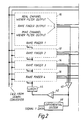
- Each Rake finger comprises a signal correlator 18 which handles an inphase signal from a down-converter, and a further signal correlator 20 which handles a quadrature phase signal from a down-converter.
- the output signal from the correlator 18 is applied to a half linear multiplier 22 by way of a one bit delay circuit 26.
- the output of the half linear multiplier 22 is applied to an input of a Wiener-like filter 30.
- the output of the Wiener-like filter 30 is applied to a multiplier 34.
- the output of the correlator 18 is also applied to a further input of the multiplier 34, the output of which is applied to a first input of an adder circuit 38.
- the output signal from the signal correlator 20 is applied to a half linear multiplier 24 by way of a one bit delay circuit 28.
- the output of the half linear multiplier 24 is applied to an input of a further Wiener-like filter 32.
- the output of the Wiener-like filter 32 is applied to an input of a multiplier 36.
- the output signal from the correlator 52 is also applied to a further input of the multiplier 36, the output of which is applied to a second input of the adder circuit 38.
- the output of the adder circuit 38 together with the output signals from the other Rake fingers 12, 14, 16 are applied to an adder circuit 40 which generates a Combined sum of the input signals for application to a decision circuit 42.
- the decision circuit 42 merely identifies whether the signal is high or low and the output of the decision circuit 42 is fed back by way of a latch circuit 44, to a second input of the respective half linear multipliers 22, 24 in the Rake finger 10 and similarly to the half linear multipliers in the other Rake fingers 12, 14, 16 to modify the signal applied to the respective Wiener filters 30, 32 in Rake finger 10 and similarly in the other Rake fingers.
- the output of the decision circuit 42 to applied to an input of a differential decode circuit 46 which is arranged to generate output data on an output line thereof.
- the circuit shown in Figure 1 uses hard decisions which are taken using the sum over ail the Rake fingers to remove the modulation from the received signal.
- the most up to date available decision is the previous one so in order to remove the modulation this must be applied to the previous sample, leading to a one sample delay.
- the delayed sample can be compensated by the previous decision.
- this must be used to provide a channel estimate for demodulation of the next sample.
- a one step predictor filter must be used and inevitably this will mean that the performance will be inferior to systems incorporating a pilot reference which can apply symmetrical filtering.
- An aim of the present invention is to provide a demodulator which does not make use of a pilot reference and in which a decision directed channel estimate can be derived from two or more signals and used to demodulate more than one signal transmitted over the same radio channel.
- apparatus for use in equipment providing a digital radio link between a fixed and a mobile radio unit, said apparatus comprising: demodulation means arranged to receive inphase and quadrature phase input signals; and estimation means for deriving a decision directed carrier reference estimate and feeding the decision directed carrier reference estimate back into said demodulation means, characterised in that said estimation means derives said decision directed carrier reference estimate from a combination of two or more signals, and said demodulation means demodulates more than one signal transmitted over the same radio channel; and in that the demodulating means includes a first demodulator comprising a plurality of Rake fingers, each of said Rake fingers including circuit means for handling inphase and quadrature phase input signals respectively, each circuit means comprising: first and second correlation means; first and second multiplying means, connected to said first and second correlation means and for receiving a feedback signal at a further input thereof; first adder means connected to an output from each first and second multiplying means; Wiener-like filter means connected to an output of said first adder means; third and fourth multiply
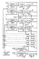
- FIG. 2 a block diagram of a borrowed reference demodulator using the DBPSK as shown, and is useful where a small number of spread spectrum signals are transmitted over a common radio channel, and if one of them is stronger than the others then the borrowed reference demodulation technique may be applied.
- the additional receiver comprises a number of Rake fingers 50, 52, 54, 56.
- Each Rake finger includes a signal correlator 58 for handling inphase components of the signal, and a further correlator 60 for handling the quadrature phase components of the signals.
- the respective inphase and quadrature phase signals are received from a down converter.
- An output from the signal correlator 58 is applied to a first input of a multiplier 62, and at a second input thereof the output from the Wiener filter 30 in the real, inphase channel is applied.
- An output from the correlator 60 is applied to a first input of a multiplier 64 and at a second input thereof there is received the output from the Wiener filter 32 in the imaginary, quadrature phase channel.
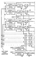
- FIG. 2 A block diagram for two equal amplitude, equal rate, signals is shown in Figure 3.
- Rake fingers 72, 74, 76, 78 each of which comprise first and second signal correlators 80, 82 for handling the inphase signal components received from a down converter and third and fourth correlators 84, 86 for handling the quadrature phase components of an input signal similarly received from a down converter.
- An output from the signal correlator 80 is connected to an input of a one bit delay circuit 88 and to a first input of a multiplier 112.
- An output from the one bit delay circuit 88 is connected to an input of a half linear multiplier 96, the output of which is connected to an adder circuit 104.
- the output of the correlator 82 is connected to an input of a one bit delay circuit 90 and to a first input of a multiplier 114.
- the output from the one bit delay circuit 90 is connected to a first input of a half linear multiplier 98, the output of which is connected to a further input of the adder circuit 104.
- the output of the adder circuit 104 is connected to an input of a Wiener filter 108, the output of which is connected to a second input of the multipliers 112, 114.
- the signal correlator 84 has an output connected to a one bit delay circuit 92 and to a first input of a multiplier 116.
- An output from the one bit delay circuit 92 is connected to a first input of a half linear multiplier 100, the output of which is connected to an input of an adder circuit 106.
- the output of the adder circuit 106 is connected to an input of a Wiener filter 110, the output of which is connected to second inputs of the multipliers 116 and 118.
- the signal correlator 86 has an output connected to an input of a one bit delay circuit 94 and to a first input of the multiplier 118.
- An output from the one bit delay circuit 94 is connected to an input of a half linear multiplier 102, the output of which is connected to a further input of the adder circuit 106.
- An output from the multipliers 112, 116 are connected to a respective input of an adder circuit 120, and the outputs from the multipliers 114, 118 are connected to a respective input of an adder circuit 122.
- the circuitry described so far is repeated in each of the Rake fingers 72, 74, 76, 78.
- the output from the adder circuit 120 and the respective outputs from the other Rake fingers are applied to an adder circuit 126 and the outputs from the adder circuit 122 and the other adder circuits in the Rake fingers are applied to an input of an adder circuit 124.
- the output from the adder circuit 126 is connected to a hard limiting device 130, the output of which is fed back to a second input of the half linear multipliers 96, 100 in each Rake finger.
- the output of the adder circuit 124 is applied to a hard limiting circuit 128, the output of which is fed back to the half linear multipliers 98, 102 in each Rake finger.
- the outputs of the adder circuits 124, 126 are also applied to a respective differential decode circuit 132, 134 respectively from which the output data is generated for each signal.
- the two signals are de-spread independently, decision corrected independently and added together to feed to the input of the channel estimation filter, that is the Wiener filters 108, 110.
- the Wiener filters 108, 110 For demodulation of equal rate signals received over the same paths this results in an approximate 3dB reduction in the mean square error for the channel estimates.
- receivers for more than two signals could be combined. It will also be appreciated that the architectures of Figures 2 and 3 could readily be combined so that pilot estimation could be achieved over any equal bit rates but applied to m > n signals where the additional signals for demodulation all had a significantly lower bit rate.
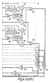
- Figure 3 can conveniently be modified as shown in Figure 4 and therefore like circuit elements have been given the same designation.
- the difference between Figures 3 and 4 is the inclusion of the sample blocks 136 and 138 between the output of the half linear multiplier 96 and the input of the adder 104, and the output of the half linear multiplier 100 and the input of the adder circuit 106, respectively.
- These blocks add together samples of the higher bit rate signalling in blocks of k samples prior to input to the Wiener filter 108, 110 respectively, in this way the rates of inputs to the adders 104, 106 respectively are matched.
- the accumulation effectively weights the high bit rate signal (stronger signal) in proportional to its amplitude in such a way that the optimum benefit is obtained from combination across the signals.
- k bit rate ratio
- the output from the adder circuit 40 is connected to a respective input of the signal correlators 48, 150, 154 which handles the signals 1, 2 and 3 respectively.
- An output from each correlator is fed to an input of a differential decode circuit 46, 152, 156 from which the data output is taken from a respective output line.
- the inputs for the half linear multipliers 26, 28 are taken from the output of the correlator 48 and is similarly fed via a hard limiting circuit 42 and a latch circuit 44.
- the outputs from each Rake finger are therefore at the chip rate rather than the bit rate.
- an additional correlator is required in order to demodulate signal 1 following the overall combiner.
- the difference between the Rake fingers of Figure 3 and Figure 6 is that the output of the Wiener filters 108, 110 are applied to a first input of a multiplier 112, 116 respectively.
- the second input of the multipliers 112, 116 receive the inphase and quadrature phase components of the input signal from the down converter respectively.
- the outputs from the Rake fingers are summed by the adder circuit 40, the output of which is applied to an input of a plurality of signal correlators 48, 150, 154 and 158 handling signals 1 to 4 respectively.
- the output of the signal correlators 154 and 158 are applied to an input of a differential decode circuit 156, 160 respectively from which the data signals 3 and 4 are generated.
- the output signals from the signal correlators 48 and 150 are applied to a hard limiting device 42, 162 respectively and to the differential decode circuits 46, 152 respectively from which the data signals 1 and 2 are generated.
- the output signals from the hard limiting devices 42, 162 are applied to a respective latch circuit 44, 162.
- the output of the latch circuit 44 is applied to the second input of the half linear multipliers 96 and 100 in each Rake finger, and similarly the output of the latch circuit 164 is applied to the second input of the half linear multipliers 98, 102 in each Rake finger.
- the signals 1 and 2 are both transmitted at the same bit rate which is higher than the rate of signals 3 and 4.
- the channel estimates are formed on the basis of decision directed demodulation of signals 1 and 2 and are then used for the purpose of rate pre-combining.
- the pre-combined signal can then be readily de-spread for demodulating of additional signals such as signals 3 and 4.
Description
- The present invention relates to apparatus for use in equipment providing a digital radio link between a fixed and a mobile radio unit.
- Equipment for providing such a radio link is described in GB-A-2276064 (GB Patent Application Number 9304901.3). This application describes the use of Wiener-like filters for providing good estimates of the amplitudes of the inphase I, and quadrature phase Q, components of, for example, a spread spectrum pilot signal.
- The problem of demodulating a spread spectrum signal using DBPSK (Dual Binary Phase Shift Keying) modulation is discussed in IEEE Transactions on Communications, Vol.37, No.3, March 1989, New York, US, pages 277-288, R.A. Iltis: 'A GLRT-Based Spread-Spectrum Receiver for Joint Channel Estimation and Interference Suppression'. Here an amplitude estimate can be made of interface and multipath. This estimate may then be used to suppress interference in a final demodulated signal.
- When demodulating DBPSK with no pilot reference it is still possible to obtain and exploit a carrier reference by means of decision directed carrier extraction. Samples are fed into the Wiener filter and are modified according to the data decisions in order to provide a reference. Published PCT Patent Application Number WO-A-94/27379, discloses a known demodulator that performs this function. It should be noted that WO-A-94/27379 is considered relevant under Art. 54(3) EPC. Figure 1 illustrates the known demodulator, as disclosed in WO-A-94/27379. The demodulator has a plurality of Rake
fingers signal correlator 18 which handles an inphase signal from a down-converter, and afurther signal correlator 20 which handles a quadrature phase signal from a down-converter. The output signal from thecorrelator 18 is applied to a halflinear multiplier 22 by way of a onebit delay circuit 26. The output of the halflinear multiplier 22 is applied to an input of a Wiener-like filter 30. The output of the Wiener-like filter 30 is applied to amultiplier 34. The output of thecorrelator 18 is also applied to a further input of themultiplier 34, the output of which is applied to a first input of an adder circuit 38. - The output signal from the
signal correlator 20 is applied to a halflinear multiplier 24 by way of a onebit delay circuit 28. The output of the halflinear multiplier 24 is applied to an input of a further Wiener-like filter 32. The output of the Wiener-like filter 32 is applied to an input of amultiplier 36. The output signal from thecorrelator 52 is also applied to a further input of themultiplier 36, the output of which is applied to a second input of the adder circuit 38. The output of the adder circuit 38 together with the output signals from theother Rake fingers adder circuit 40 which generates a Combined sum of the input signals for application to adecision circuit 42. Thedecision circuit 42 merely identifies whether the signal is high or low and the output of thedecision circuit 42 is fed back by way of alatch circuit 44, to a second input of the respective halflinear multipliers finger 10 and similarly to the half linear multipliers in theother Rake fingers Wiener filters finger 10 and similarly in the other Rake fingers. The output of thedecision circuit 42 to applied to an input of adifferential decode circuit 46 which is arranged to generate output data on an output line thereof. - The circuit shown in Figure 1 uses hard decisions which are taken using the sum over ail the Rake fingers to remove the modulation from the received signal. The most up to date available decision is the previous one so in order to remove the modulation this must be applied to the previous sample, leading to a one sample delay. The delayed sample can be compensated by the previous decision. However, this must be used to provide a channel estimate for demodulation of the next sample. Thus a one step predictor filter must be used and inevitably this will mean that the performance will be inferior to systems incorporating a pilot reference which can apply symmetrical filtering.
- An aim of the present invention is to provide a demodulator which does not make use of a pilot reference and in which a decision directed channel estimate can be derived from two or more signals and used to demodulate more than one signal transmitted over the same radio channel.
- According to the present invention there is provided apparatus for use in equipment providing a digital radio link between a fixed and a mobile radio unit, said apparatus comprising: demodulation means arranged to receive inphase and quadrature phase input signals; and estimation means for deriving a decision directed carrier reference estimate and feeding the decision directed carrier reference estimate back into said demodulation means,
characterised in that said estimation means derives said decision directed carrier reference estimate from a combination of two or more signals, and said demodulation means demodulates more than one signal transmitted over the same radio channel; and
in that the demodulating means includes a first demodulator comprising a plurality of Rake fingers, each of said Rake fingers including circuit means for handling inphase and quadrature phase input signals respectively, each circuit means comprising: first and second correlation means; first and second multiplying means, connected to said first and second correlation means and for receiving a feedback signal at a further input thereof; first adder means connected to an output from each first and second multiplying means; Wiener-like filter means connected to an output of said first adder means; third and fourth multiplying means for generating a product of an output from the Wiener-like filter means with an output from said first and second correlation means; each of said Rake fingers further including second adder means connected to an output from each third multiplying means; and third adder means connected to an output from each fourth multiplying means; an output from said second adder means in each Rake finger being connected to a first input of said estimation means and an output from said third adder means in each Rake finger being connected to a second input of the estimation means, said estimation means including: fourth adder means and fifth adder means, for receiving outputs from each of said second adder means and said third adder means respectively, an output of said fourth adder means being fed back to said first multiplying means by way of a limiting device and an output of the fifth adder means being fed back to said second multiplying means by way of a limiting device; and decoding means for generating respective first and second data signals. - Various embodiments of the present invention will now be described with reference to the accompanying drawings, wherein:
- FIGURE 1 shows a block diagram of a known form of demodulator,
- FIGURE 2 shows a block diagram of a borrowed reference demodulator,
- FIGURE 3 shows a block diagram of a shared reference demodulator.
- FIGURE 4 shows a block diagram of a shared reference demodulator operating at difference bit rates.
- FIGURE 5 shows a block diagram of a borrowed referenced demodulator using pre-combining Rake architecture, and
- FIGURE 6 shows a borrowed reference demodulator using pre-combining Rake architecture with shared pilot generation.
-
- Referring to Figure 2 a block diagram of a borrowed reference demodulator using the DBPSK as shown, and is useful where a small number of spread spectrum signals are transmitted over a common radio channel, and if one of them is stronger than the others then the borrowed reference demodulation technique may be applied.
- In Figure 2, the demodulation of two signals is considered although it will be appreciated by those skilled in the art that the architecture may be readily extended to more signals.
- In Figure 2, the architecture shown on the left hand side of the diagram is almost identical to that of Figure 1 and therefore similar components bear the same reference numeral as shown in Figure 1. The only difference is that the Wiener filter outputs are brought out to provide channel estimates for the receiver shown on the right hand side of Figure 2. The circuitry for demodulation of the second signal is therefore dimmer requiring neither Wiener filters nor decision directed removal of data. Moreover, if the mean power of
signal 1 is greater than that ofsignal 2, as would be the case if the bit rate of the two signals was different, then the channel estimate provided fromsignal 1 will be more accurate than could have been provided fromsignal 2. It will be readily appreciated that additional receivers each with the same architecture as the receiver forsignal 2, could be added for demodulation of further spread spectrum signals. - The additional receiver comprises a number of
Rake fingers signal correlator 58 for handling inphase components of the signal, and afurther correlator 60 for handling the quadrature phase components of the signals. The respective inphase and quadrature phase signals are received from a down converter. An output from thesignal correlator 58 is applied to a first input of amultiplier 62, and at a second input thereof the output from the Wienerfilter 30 in the real, inphase channel is applied. An output from thecorrelator 60 is applied to a first input of amultiplier 64 and at a second input thereof there is received the output from the Wienerfilter 32 in the imaginary, quadrature phase channel. The outputs from themultipliers further adder circuit 68. Theadder circuit 68 receives the outputs from eachRake finger differential decode circuit 70 from which is generated the data indicative of the second signal. - The architecture as shown in Figure 2 is based on the assumption that the first signal was stronger than all of the others. If this is not the case then significant benefits can be obtained by deriving a single, common channel reference from the combination of the two, or more, signals. A block diagram for two equal amplitude, equal rate, signals is shown in Figure 3.
- Referring to Figure 3, a plurality of Rake fingers are shown 72, 74, 76, 78 each of which comprise first and
second signal correlators fourth correlators signal correlator 80 is connected to an input of a onebit delay circuit 88 and to a first input of amultiplier 112. An output from the onebit delay circuit 88 is connected to an input of a halflinear multiplier 96, the output of which is connected to anadder circuit 104. - The output of the
correlator 82 is connected to an input of a onebit delay circuit 90 and to a first input of amultiplier 114. The output from the onebit delay circuit 90 is connected to a first input of a halflinear multiplier 98, the output of which is connected to a further input of theadder circuit 104. The output of theadder circuit 104 is connected to an input of aWiener filter 108, the output of which is connected to a second input of themultipliers signal correlator 84 has an output connected to a onebit delay circuit 92 and to a first input of amultiplier 116. An output from the onebit delay circuit 92 is connected to a first input of a halflinear multiplier 100, the output of which is connected to an input of anadder circuit 106. The output of theadder circuit 106 is connected to an input of aWiener filter 110, the output of which is connected to second inputs of themultipliers signal correlator 86 has an output connected to an input of a onebit delay circuit 94 and to a first input of themultiplier 118. An output from the onebit delay circuit 94 is connected to an input of a halflinear multiplier 102, the output of which is connected to a further input of theadder circuit 106. An output from themultipliers adder circuit 120, and the outputs from themultipliers adder circuit 122. The circuitry described so far is repeated in each of theRake fingers adder circuit 120 and the respective outputs from the other Rake fingers are applied to anadder circuit 126 and the outputs from theadder circuit 122 and the other adder circuits in the Rake fingers are applied to an input of anadder circuit 124. The output from theadder circuit 126 is connected to a hard limitingdevice 130, the output of which is fed back to a second input of the halflinear multipliers adder circuit 124 is applied to a hard limitingcircuit 128, the output of which is fed back to the halflinear multipliers adder circuits differential decode circuit - In the architecture shown in Figure 3, the two signals are de-spread independently, decision corrected independently and added together to feed to the input of the channel estimation filter, that is the Wiener filters 108, 110. For demodulation of equal rate signals received over the same paths this results in an approximate 3dB reduction in the mean square error for the channel estimates.
- It will be appreciated that receivers for more than two signals could be combined. It will also be appreciated that the architectures of Figures 2 and 3 could readily be combined so that pilot estimation could be achieved over any equal bit rates but applied to m > n signals where the additional signals for demodulation all had a significantly lower bit rate.
- If more than two equal bit rate signals are combined then a greater improvement in the channel reference will arise. The demodulator described with reference to Figure 3 is most usefully applied to the case of equal bit rate signals but is not restricted to this case.
- Consider the case of two signals, signal 1 operating at bit K x B kbps and
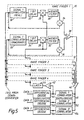
signal 2 operating a B kbps. To accommodate these different bit rates Figure 3 can conveniently be modified as shown in Figure 4 and therefore like circuit elements have been given the same designation. The difference between Figures 3 and 4 is the inclusion of the sample blocks 136 and 138 between the output of the halflinear multiplier 96 and the input of theadder 104, and the output of the halflinear multiplier 100 and the input of theadder circuit 106, respectively. These blocks add together samples of the higher bit rate signalling in blocks of k samples prior to input to theWiener filter adders - Any of the above embodiments may be implemented using a pre-combining Rake architecture, and may be used for decision directed reference extraction and for the demodulation of multiple signals. The architecture which achieves this is shown in Figure 5. Figure 5 is very similar to Figure 1 and like circuit elements have been given the same reference numeral.
- In Figure 5 the output from the
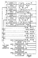
adder circuit 40 is connected to a respective input of thesignal correlators signals differential decode circuit linear multipliers correlator 48 and is similarly fed via a hard limitingcircuit 42 and alatch circuit 44. The outputs from each Rake finger are therefore at the chip rate rather than the bit rate. Thus, an additional correlator is required in order to demodulatesignal 1 following the overall combiner. The benefit of such an architecture is that now, additional signals can be readily demodulated with just the addition of a further real correlator and a differential decoder for each additional signal as shown. Thecorrelator 150 and thedifferential decode circuit 152 handles signal 2 and thecorrelator 154 and thedifferential decode circuit 156 handles thesignal 3. - Clearly the functionality of Figure 5 could be combined with that of Figure 3 or 4 to enable the pre-combining to be performed on the basis of more than one signal whilst allowing multiplicity of additional lower bit rate signals to be demodulated. The architecture for the case of combining Figure 5 with Figure 3 is illustrated in Figure 6, and like circuit elements have been given the same reference numeral.
- The difference between the Rake fingers of Figure 3 and Figure 6 is that the output of the Wiener filters 108, 110 are applied to a first input of a
multiplier multipliers adder circuit 40, the output of which is applied to an input of a plurality ofsignal correlators handling signals 1 to 4 respectively. The output of the signal correlators 154 and 158 are applied to an input of adifferential decode circuit device differential decode circuits devices respective latch circuit latch circuit 44 is applied to the second input of the halflinear multipliers latch circuit 164 is applied to the second input of the halflinear multipliers - The
signals signals signals signals
Claims (5)
- Apparatus for use in equipment providing a digital radio link between a fixed and a mobile radio unit, said apparatus comprising:characterised in that said estimation means derives said decision directed carrier reference estimate from a combination of two or more signals, and said demodulation means demodulates more than one signal transmitted over the same radio channel; anddemodulation means (50, 52, 54, 56; 72, 74, 76, 78) arranged to receive inphase and quadrature phase input signals; andestimation means (124, 126, 128, 130, 132, 134; 40, 42, 46, 48, 150, 152, 154, 156; 162) for deriving a decision directed carrier reference estimate and feeding the decision directed carrier reference estimate back into said demodulation means,
in that the demodulating means includes a first demodulator (72, 74, 76, 78) comprising a plurality of Rake fingers (72, 74, 76, 78), each of said Rake fingers including circuit means for handling inphase and quadrature phase input signals respectively, each circuit means comprising:an output from said second adder means (120) in each Rake finger (72, 74, 76, 78) being connected to a first input of said estimation means (40, 42, 46; 124, 126, 128, 130, 132, 134; 48, 150, 152, 154, 156; 162) and an output from said third adder means (122) in each Rake finger (72, 74, 76, 78) being connected to a second input of the estimation means (40, 42, 46; 124, 126, 128, 130, 132, 134; 48, 150, 152, 154, 156; 162),first and second correlation means (80, 82, 84, 86);first and second multiplying means (96, 98, 100, 102), connected to said first and second correlation means (80, 82, 84, 86) and for receiving a feedback signal at a further input thereof;first adder means (104, 106) connected to an output from each first and second multiplying means (96, 98, 100, 102);Wiener-like filter means (108, 110) connected to an output of said first adder means (104, 106);third and fourth multiplying means (112, 114, 116, 118) for generating a product of an output from the Wiener-like filter means (108, 110) with an output from said first and second correlation means (80, 82, 84, 86);each of said Rake fingers further including second adder means (120) connected to an output from each third multiplying means (112, 116); andthird adder means (122) connected to an output from each fourth multiplying means (114, 118);
said estimation means (40, 42, 46; 124, 126, 128, 130, 132, 134; 48, 150, 152, 154, 156; 162) including:fourth adder means (126) and fifth adder means (124), for receiving outputs from each of said second adder means (120) and said third adder means (122) respectively, an output of said fourth adder means (126) being fed back to said first multiplying means (96, 100) by way of a limiting device (130) and an output of the fifth adder means (124) being fed back to said second multiplying means (98, 102) by way of a limiting device (128); anddecoding means (132, 134) for generating respective first and second data signals. - Apparatus as claimed in Claim 1, wherein the output of each first multiplying means (96, 100) is connected to said first adder means (104, 106) by way of accumulation means (136, 138) arranged to add together samples of a higher bit rate signal in blocks of k samples.
- Apparatus as claimed in Claims 1 or 2, wherein said demodulating means (50, 52, 54, 56; 72, 74, 76, 78) further includes at least one further demodulator (50, 52, 54, 56) for handling a plurality of spread spectrum signals transmitted over a common radio channel, each further demodulator (50, 52, 54, 56) comprising a plurality of Rake fingers (50, 52, 54, 56), each Rake finger including:first and second correlation means (58, 60) for receiving said inphase and quadrature phase input signals respectively;first multiplying means (62) for generating a product of an output from said first correlation means (58) with an output from said Wiener-like filter means (108) associated with said inphase signal in a corresponding Rake finger of said first demodulator (72, 74, 76, 78);second multiplying means (64) for generating a product of an output from said second correlation means (60) with an output from said Wiener-like filter means (110) associated with said quadrature phase signal in a corresponding Rake finger of said first demodulator (72, 74, 76, 78); andadder means (66) for summing said outputs from said first and second multiplying means (62, 64).
- Apparatus as claimed in Claim 3, wherein said estimation means further comprises further adder means (68) for summing said output from each adder means (66) in each Rake finger (50, 52, 54, 56) of said at least one further demodulator to provide an output for application to decode means (70) for generating data relating to a third signal.
- Apparatus as claimed in any one of the preceding claims, wherein said output from at least one of said fourth adder means (126) and said fifth adder means (124) is further connected to at least a third and a fourth correlation means (48, 154) each having an output connected to a respective decoding means (46, 156) from which output data signals are generated respectively, an output from said third correlation means (48) being fed back to said first demodulator by way of a limiting device (42).
Applications Claiming Priority (2)
| Application Number | Priority Date | Filing Date | Title |
|---|---|---|---|
| GB9317781A GB2281482B (en) | 1993-08-26 | 1993-08-26 | Apparatus for use in equipment providing a digital radio link between a fixed and a mobile radio unit |
| GB9317781 | 1993-08-26 |
Publications (2)
| Publication Number | Publication Date |
|---|---|
| EP0641091A1 EP0641091A1 (en) | 1995-03-01 |
| EP0641091B1 true EP0641091B1 (en) | 2002-03-20 |
Family
ID=10741088
Family Applications (1)
| Application Number | Title | Priority Date | Filing Date |
|---|---|---|---|
| EP94110653A Expired - Lifetime EP0641091B1 (en) | 1993-08-26 | 1994-07-08 | Apparatus using decision directed channel estimation in a digital mobile radio link |
Country Status (7)
| Country | Link |
|---|---|
| US (1) | US5594755A (en) |
| EP (1) | EP0641091B1 (en) |
| JP (1) | JPH0786985A (en) |
| CN (1) | CN1108835A (en) |
| DE (1) | DE69430160T2 (en) |
| GB (1) | GB2281482B (en) |
| IN (1) | IN188216B (en) |
Families Citing this family (12)
| Publication number | Priority date | Publication date | Assignee | Title |
|---|---|---|---|---|
| GB2293730B (en) * | 1994-09-28 | 1998-08-05 | Roke Manor Research | Apparatus for use in equipment providing a digital radio link between a fixed and a mobile radio unit |
| FI97581C (en) * | 1995-02-10 | 1997-01-10 | Nokia Telecommunications Oy | Receiver and method for generating spreading codes at the receiver |
| US5764688A (en) * | 1995-06-30 | 1998-06-09 | Roke Manor Research Limited | Apparatus for use in equipment providing a digital radio link between a fixed and a mobile radio unit |
| US5677930A (en) * | 1995-07-19 | 1997-10-14 | Ericsson Inc. | Method and apparatus for spread spectrum channel estimation |
| US5768307A (en) * | 1996-09-13 | 1998-06-16 | Telefonaktiebolaget Lm Ericsson | Coherent demodulation with decision-directed channel estimation for digital communication |
| US5914949A (en) * | 1996-12-17 | 1999-06-22 | Lucent Technologies Inc. | Circuit and method for tracking finger off-set in a spread-spectrum rake receiver and wireless infrastructure employing the same |
| US5983105A (en) * | 1997-03-17 | 1999-11-09 | Nokia Telecommunications Oy | Method and receiver implemented on the rake principle |
| JP2870526B1 (en) * | 1997-09-04 | 1999-03-17 | 日本電気株式会社 | CDMA receiver |
| US6229839B1 (en) * | 1999-02-08 | 2001-05-08 | Qualcomm Incorporated | Method and apparatus for time tracking |
| FR2814877B1 (en) * | 2000-10-02 | 2003-01-03 | Mitsubishi Electric Inf Tech | CHANNEL ESTIMATION SEQUENCE AND METHOD OF ESTIMATING A TRANSMISSION CHANNEL WHICH USES SUCH A CHANNEL ESTIMATION SEQUENCE |
| KR100427577B1 (en) * | 2001-12-27 | 2004-04-28 | 한국전자통신연구원 | Hardware-efficient rake receiver |
| CN101232304B (en) * | 2008-02-29 | 2012-05-30 | 北京邮电大学 | Equipment and method for sending and receiving channel information in communication system |
Citations (1)
| Publication number | Priority date | Publication date | Assignee | Title |
|---|---|---|---|---|
| WO1994027379A1 (en) * | 1993-05-12 | 1994-11-24 | Roke Manor Research Limited | Dual-pass rake receiver for a digital radio link between a fixed and a mobile radio unit |
Family Cites Families (2)
| Publication number | Priority date | Publication date | Assignee | Title |
|---|---|---|---|---|
| US5519730A (en) * | 1990-06-12 | 1996-05-21 | Jasper; Steven C. | Communication signal having a time domain pilot component |
| US5361276A (en) * | 1993-09-13 | 1994-11-01 | At&T Bell Laboratories | All digital maximum likelihood based spread spectrum receiver |
-
1993
- 1993-08-26 GB GB9317781A patent/GB2281482B/en not_active Expired - Fee Related
-
1994
- 1994-07-08 EP EP94110653A patent/EP0641091B1/en not_active Expired - Lifetime
- 1994-07-08 DE DE69430160T patent/DE69430160T2/en not_active Expired - Fee Related
- 1994-08-05 IN IN743MA1994 patent/IN188216B/en unknown
- 1994-08-18 US US08/292,040 patent/US5594755A/en not_active Expired - Fee Related
- 1994-08-26 CN CN94115732.6A patent/CN1108835A/en active Pending
- 1994-08-26 JP JP6202343A patent/JPH0786985A/en active Pending
Patent Citations (1)
| Publication number | Priority date | Publication date | Assignee | Title |
|---|---|---|---|---|
| WO1994027379A1 (en) * | 1993-05-12 | 1994-11-24 | Roke Manor Research Limited | Dual-pass rake receiver for a digital radio link between a fixed and a mobile radio unit |
Also Published As
| Publication number | Publication date |
|---|---|
| EP0641091A1 (en) | 1995-03-01 |
| GB2281482A (en) | 1995-03-01 |
| GB9317781D0 (en) | 1993-10-13 |
| DE69430160D1 (en) | 2002-04-25 |
| IN188216B (en) | 2002-08-31 |
| GB2281482B (en) | 1997-10-22 |
| US5594755A (en) | 1997-01-14 |
| DE69430160T2 (en) | 2002-10-31 |
| JPH0786985A (en) | 1995-03-31 |
| CN1108835A (en) | 1995-09-20 |
Similar Documents
| Publication | Publication Date | Title |
|---|---|---|
| EP0671082B2 (en) | Dot product circuit for multipath receivers | |
| US8553820B2 (en) | Groupwise successive interference cancellation for block transmission with reception diversity | |
| CA2258376C (en) | Cdma multiuser receiver featuring a combination of array antenna and multiuser cancelers | |
| CA2195176C (en) | Signal demodulation and diversity combining in a communications system using orthogonal modulation | |
| US5383220A (en) | Data demodulator of a receiving apparatus for spread spectrum communication | |
| US7310305B2 (en) | Method for determining reference phase in radio communication system which uses orthogonal M-ary modulation, and coherent detection method using the same | |
| KR19980032939A (en) | Interference signal canceller | |
| KR20020004878A (en) | Code division multiple access wireless system with time reversed space time block transmitter diversity encoding | |
| EP0641091B1 (en) | Apparatus using decision directed channel estimation in a digital mobile radio link | |
| US7336640B2 (en) | Method and apparatus for CDMA demodulation | |
| US20020159505A1 (en) | Receiver and receiving method fro spread spectrum communication | |
| US7003020B2 (en) | Selection of multiple propagation paths by successive removal and detection of high autocorrelations | |
| US7027491B2 (en) | Interference cancellation receiver for use in a CDMA system | |
| US7586980B2 (en) | Apparatus for coherent combining type demodulation in communication system and method thereof | |
| EP1164711A2 (en) | Receiving apparatus for spread spectrum transmission antenna diversity | |
| KR100358349B1 (en) | Apparatus and Method of Group-wise Parallel Interference Cancellation for Multi-rate DS-CDMA Systems | |
| WO1994027379A1 (en) | Dual-pass rake receiver for a digital radio link between a fixed and a mobile radio unit | |
| GB2278029A (en) | Apparatus for use in digital radio equipment | |
| MXPA98006794A (en) | Method and apparatus for the demodulation of signal and the combination in diversity of modulated signals ortogonalme | |
| JPH0795130A (en) | Spread spectrum signal receiver | |
| JPH11225094A (en) | Spread spectrum communication receiver | |
| MXPA99004498A (en) | Despreading of direct sequence spread spectrum communications signals |
Legal Events
| Date | Code | Title | Description |
|---|---|---|---|
| PUAI | Public reference made under article 153(3) epc to a published international application that has entered the european phase |
Free format text: ORIGINAL CODE: 0009012 |
|
| AK | Designated contracting states |
Kind code of ref document: A1 Designated state(s): DE ES FR GB IT |
|
| 17P | Request for examination filed |
Effective date: 19950711 |
|
| 17Q | First examination report despatched |
Effective date: 19990705 |
|
| GRAG | Despatch of communication of intention to grant |
Free format text: ORIGINAL CODE: EPIDOS AGRA |
|
| GRAG | Despatch of communication of intention to grant |
Free format text: ORIGINAL CODE: EPIDOS AGRA |
|
| GRAG | Despatch of communication of intention to grant |
Free format text: ORIGINAL CODE: EPIDOS AGRA |
|
| GRAH | Despatch of communication of intention to grant a patent |
Free format text: ORIGINAL CODE: EPIDOS IGRA |
|
| GRAH | Despatch of communication of intention to grant a patent |
Free format text: ORIGINAL CODE: EPIDOS IGRA |
|
| REG | Reference to a national code |
Ref country code: GB Ref legal event code: IF02 |
|
| GRAA | (expected) grant |
Free format text: ORIGINAL CODE: 0009210 |
|
| AK | Designated contracting states |
Kind code of ref document: B1 Designated state(s): DE ES FR GB IT |
|
| REF | Corresponds to: |
Ref document number: 69430160 Country of ref document: DE Date of ref document: 20020425 |
|
| PGFP | Annual fee paid to national office [announced via postgrant information from national office to epo] |
Ref country code: GB Payment date: 20020703 Year of fee payment: 9 |
|
| PGFP | Annual fee paid to national office [announced via postgrant information from national office to epo] |
Ref country code: FR Payment date: 20020709 Year of fee payment: 9 |
|
| PGFP | Annual fee paid to national office [announced via postgrant information from national office to epo] |
Ref country code: DE Payment date: 20020717 Year of fee payment: 9 |
|
| ET | Fr: translation filed | ||
| ET | Fr: translation filed | ||
| PG25 | Lapsed in a contracting state [announced via postgrant information from national office to epo] |
Ref country code: ES Free format text: LAPSE BECAUSE OF FAILURE TO SUBMIT A TRANSLATION OF THE DESCRIPTION OR TO PAY THE FEE WITHIN THE PRESCRIBED TIME-LIMIT Effective date: 20020925 |
|
| PLBE | No opposition filed within time limit |
Free format text: ORIGINAL CODE: 0009261 |
|
| STAA | Information on the status of an ep patent application or granted ep patent |
Free format text: STATUS: NO OPPOSITION FILED WITHIN TIME LIMIT |
|
| 26N | No opposition filed |
Effective date: 20021223 |
|
| PG25 | Lapsed in a contracting state [announced via postgrant information from national office to epo] |
Ref country code: GB Free format text: LAPSE BECAUSE OF NON-PAYMENT OF DUE FEES Effective date: 20030708 |
|
| PG25 | Lapsed in a contracting state [announced via postgrant information from national office to epo] |
Ref country code: DE Free format text: LAPSE BECAUSE OF NON-PAYMENT OF DUE FEES Effective date: 20040203 |
|
| GBPC | Gb: european patent ceased through non-payment of renewal fee |
Effective date: 20030708 |
|
| PG25 | Lapsed in a contracting state [announced via postgrant information from national office to epo] |
Ref country code: FR Free format text: LAPSE BECAUSE OF NON-PAYMENT OF DUE FEES Effective date: 20040331 |
|
| REG | Reference to a national code |
Ref country code: FR Ref legal event code: ST |
|
| PG25 | Lapsed in a contracting state [announced via postgrant information from national office to epo] |
Ref country code: IT Free format text: LAPSE BECAUSE OF NON-PAYMENT OF DUE FEES;WARNING: LAPSES OF ITALIAN PATENTS WITH EFFECTIVE DATE BEFORE 2007 MAY HAVE OCCURRED AT ANY TIME BEFORE 2007. THE CORRECT EFFECTIVE DATE MAY BE DIFFERENT FROM THE ONE RECORDED. Effective date: 20050708 |