EP0638941A2 - Phototransistor with quantum well base structure - Google Patents
Phototransistor with quantum well base structure Download PDFInfo
- Publication number
- EP0638941A2 EP0638941A2 EP94305747A EP94305747A EP0638941A2 EP 0638941 A2 EP0638941 A2 EP 0638941A2 EP 94305747 A EP94305747 A EP 94305747A EP 94305747 A EP94305747 A EP 94305747A EP 0638941 A2 EP0638941 A2 EP 0638941A2
- Authority
- EP
- European Patent Office
- Prior art keywords
- layer
- layers
- quantum well
- doped
- phototransistor
- Prior art date
- Legal status (The legal status is an assumption and is not a legal conclusion. Google has not performed a legal analysis and makes no representation as to the accuracy of the status listed.)
- Withdrawn
Links
Images

Classifications
-
- B—PERFORMING OPERATIONS; TRANSPORTING
- B82—NANOTECHNOLOGY
- B82Y—SPECIFIC USES OR APPLICATIONS OF NANOSTRUCTURES; MEASUREMENT OR ANALYSIS OF NANOSTRUCTURES; MANUFACTURE OR TREATMENT OF NANOSTRUCTURES
- B82Y20/00—Nanooptics, e.g. quantum optics or photonic crystals
-
- H—ELECTRICITY
- H10—SEMICONDUCTOR DEVICES; ELECTRIC SOLID-STATE DEVICES NOT OTHERWISE PROVIDED FOR
- H10F—INORGANIC SEMICONDUCTOR DEVICES SENSITIVE TO INFRARED RADIATION, LIGHT, ELECTROMAGNETIC RADIATION OF SHORTER WAVELENGTH OR CORPUSCULAR RADIATION
- H10F30/00—Individual radiation-sensitive semiconductor devices in which radiation controls the flow of current through the devices, e.g. photodetectors
- H10F30/20—Individual radiation-sensitive semiconductor devices in which radiation controls the flow of current through the devices, e.g. photodetectors the devices having potential barriers, e.g. phototransistors
- H10F30/21—Individual radiation-sensitive semiconductor devices in which radiation controls the flow of current through the devices, e.g. photodetectors the devices having potential barriers, e.g. phototransistors the devices being sensitive to infrared, visible or ultraviolet radiation
- H10F30/24—Individual radiation-sensitive semiconductor devices in which radiation controls the flow of current through the devices, e.g. photodetectors the devices having potential barriers, e.g. phototransistors the devices being sensitive to infrared, visible or ultraviolet radiation the devices having only two potential barriers, e.g. bipolar phototransistors
- H10F30/245—Bipolar phototransistors
-
- H—ELECTRICITY
- H10—SEMICONDUCTOR DEVICES; ELECTRIC SOLID-STATE DEVICES NOT OTHERWISE PROVIDED FOR
- H10F—INORGANIC SEMICONDUCTOR DEVICES SENSITIVE TO INFRARED RADIATION, LIGHT, ELECTROMAGNETIC RADIATION OF SHORTER WAVELENGTH OR CORPUSCULAR RADIATION
- H10F77/00—Constructional details of devices covered by this subclass
- H10F77/10—Semiconductor bodies
- H10F77/14—Shape of semiconductor bodies; Shapes, relative sizes or dispositions of semiconductor regions within semiconductor bodies
- H10F77/146—Superlattices; Multiple quantum well structures
- H10F77/1465—Superlattices; Multiple quantum well structures including only Group IV materials, e.g. Si-SiGe superlattices
Definitions
- This invention relates to phototransistors and more particularly to phototransistors that are useful in the long wavelength infrared region, that is for wavelengths of about 6 to 20 micrometers.
- Heterojunction bipolar phototransistors are well known as devices that can be used to produce an output electrical current in response to the presence of light. See, for example, the article entitled “Gain of a Heterojunction Bipolar Phototransistor” by Naresh Chand et al. in IEEE Transactions on Electron Devices, Vol ED-32, No. 3, March 1985, pages 622-627. In the Chand et al. article, a phototransistor is described wherein the incident light passes through a transparent emitter and is absorbed in the base, the depletion region between the base and the collector, and the neutral collector.
- the electron-hole pairs generated in the depletion region and within the diffusion lengths of the minority carriers in the base and collector are separated and collected by the field of the base-collector junction leading to a current flow in an external circuit.
- the holes are swept into the base and are accumulated near the emitter-base junction due to a large potential barrier in the valence band at the heterointerface until they recombine with injected electrons from the emitter.
- a large injection of electrons occurs from the emitter into the base resulting in a large electron-current flow from the emitter to the collector.
- phototransistors of the type in the Chand et al. article have provided greater gain than a simple photodiode, they have not provided a light detection that is useful in the infrared region of about 6 to 20 micrometers wavelength.
- quantum well infrared detector wherein p-doped Si 1-x Ge x layers are grown between undoped Si barrier layers in a quantum well structure in order to form multiple quantum wells primarily in the valence band.
- quantum well structure in this context refers to stacks of ultrathin layers of semiconductor material where the dimension of the ultrathin layer is sufficiently small such that the electron is considered to be essentially confined in that dimension by the energy barriers created by the differences in bandgaps.
- a description of this type of a photodetector can be found, for example, in the article entitled "Si 1-x Ge x /Si multiple quantum well infrared detector", by R. P. G.
- a high gain, high detectivity long wavelength infrared photodetector with lower leakage and lower dark current is provided by the present invention wherein the base region of a phototransistor is constructed with a plurality of alternating layers of semiconductor material such that a quantum well structure is created in the base region with doping in the quantum wells giving them a conductivity opposite to that in the emitter and collector regions of the phototransistor.
- the semiconductor materials are preferably chosen such that most of the bandgap discontinuity creating the quantum wells is in the valence band. Accordingly, efficient operation of the phototransistor is achieved since there is a lack of conduction band discontinuity and there is therefore no impediment to the transport of electrons in the conduction band.
- the quantum well closest to the emitter-base junction of the transistor is constructed so as to be wider and deeper than the other quantum wells thereby providing higher hole confinement near the emitter-base junction and therefore increasing the current flow out of the emitter into the base region.
- the barrier layer between the last quantum well and the base-collector junction is doped with a material so as to produce a conductivity in this layer which is opposite to that in the collector region in order to reduce the leakage current of the base-collector junction.
- the long wavelength infrared photodetector constructed in accordance with the present invention is essentially an npn transistor in which the base region consists of a quantum well structure constructed of alternating layers of silicon germanium (Si 1-x Ge x ) and silicon (Si). These alternating layers of SiGe and Si provide a sequence of quantum wells primarily in the valance band as described hereinafter in connection with Fig. 2.
- the phototransistor is fabricated by first growing an approximately 1 ⁇ m (micrometer) thick Si layer 101 with n-type doping on a highly resistive Si substrate 100 to form the collector region of the phototransistor.
- This layer 101 is n-doped at a level of about 2 X 1018 cm ⁇ 3 for the first 0.5 ⁇ m of growth and at a level of about 1 X 1016 cm ⁇ 3 in the remaining 0.5 ⁇ m.
- a Si layer 103 with a p-type doping level of about 5 X 1017 cm ⁇ 3 is grown to a thickness of about 300 ⁇ onto layer 101.
- Layer 103 is p-doped in order to reduce the leakage current of the base-collector junction.
- a p-doped Si 1-x Ge x layer 104 is grown with a thickness of about 40 ⁇ on layer 103 followed by an undoped Si layer 105.
- This process of alternately growing layers of Si 1-x Ge x followed by layers of undoped Si is then repeated to form layers 106-115 in Fig. 1. All of the undoped Si layers are grown with a thickness of about 300 ⁇ , and the Si 1-x Ge x layers described thus far are grown with thicknesses of about 40 ⁇ and p-doped with levels of about 2 X 1018 cm ⁇ 3, where the germanium mole fractions (x) are about 20 percent.
- layer 103 may be eliminated, and layer 104 can be grown directly on collector layer 101 without departing from the spirit and scope of the present invention. Since layer 104 is also p-doped, it will also function so as to reduce the leakage current of the base-collector junction.
- the final Si 1-x Ge x layer 116 is grown on layer 115 and is also p-doped to a level of about 2 X 1018 cm ⁇ 3, but it is grown with a larger thickness of about 60 ⁇ and a larger germanium mole fraction (x) of about 25 percent in order to provide a wider and deeper quantum well in the valance band than the quantum wells provided by the even-numbered layers 104 through 114.
- x germanium mole fraction
- n-doped layer 117 is grown on layer 116 to form the emitter region with n-type doping levels of about 2 X 1017 cm ⁇ 3.
- the entire grown structure is then masked and etched so as to expose the collector layer 101 onto which a metallic contact 102 is deposited in order to provide a connection to the collector region.
- a metallic contact 118 is also deposited on layer 117 in order to provide a connection to the emitter region.
- Both layers 101 and 117 are much, much thicker than layers 103 through 116, and therefor only segments of layers 101 and 117 are shown in Fig. 1 to avoid misrepresenting their thicknesses relative to the layers in the base region.
- an external power source 120 in Fig. 1 has its positive terminal directly connected to contact 102 and its negative terminal connected through a load impedance 119 to the contact 118.
- the infrared light beam to be detected shown as 125 in Fig. 1, is coupled through the back of substrate 100 passing through the collector region into the base region which consists of layers 103 through 116.
- the bandgap differences between the Si and the Si 1-x Ge x layers provide quantum wells primarily in the valance band, and the conduction band has essentially no discontinuity thereby permitting unimpeded transport of electrons in the base and therefor efficient operation of the transistor.
- the infrared light beam 125 is coupled through the collector region (layer 101) and through absorption excites a hole from a bound state in a SiGe quantum well either to a higher state within the well or to the continuum above the barriers provided by the odd-numbered Si layers 103-115.
- the quantum wells of Fig. 2 are designated by numbers which are identical to the layers which produce them except that the hundreds digit has been changed from one hundred in Fig. 1 to two hundred in fig. 2.
- the quantum well produced by layer 116 in Fig. 1 is designated as quantum well 216 in Fig. 2 and is shown as being wider and deeper than the other quantum wells.
- the device described hereinabove operates in a two-terminal mode.
- the holes lost due to recombination with minority carrier electrons will largely be replaced by injection of holes from the collector and by thermal generation in the base-collector depletion region.
- the most efficient method of replacing the lost holes would, however, be a small continuous wave or pulsed light bias whose wavelength should match the bandgap of the SiGe quantum well. Such a light bias will make the device equivalent to a three terminal device.
- the optical gain, g ⁇ ⁇ ⁇
- the holes are excited but the current transport in the base is through the electrons which occurs both by diffusion and drift.
- the device has a reversed biased p/n junction between the base and collector regions which causes the amount of leakage current to be much smaller than prior art quantum well devices which have no p/n junctions.
- the proposed device is accordingly expected to operate at relatively higher temperatures. Because the proposed photodetector has gain, the associated electronics can be reduced significantly. Furthermore, since the proposed photodetector is based on a silicon materials system, silicon electronics can be placed on the same substrate thereby resulting in less complex and more reliable circuits.
Landscapes
- Chemical & Material Sciences (AREA)
- Engineering & Computer Science (AREA)
- Nanotechnology (AREA)
- Physics & Mathematics (AREA)
- Life Sciences & Earth Sciences (AREA)
- Biophysics (AREA)
- Optics & Photonics (AREA)
- Crystallography & Structural Chemistry (AREA)
- Light Receiving Elements (AREA)
Abstract
Description
- This invention relates to phototransistors and more particularly to phototransistors that are useful in the long wavelength infrared region, that is for wavelengths of about 6 to 20 micrometers.
- Heterojunction bipolar phototransistors are well known as devices that can be used to produce an output electrical current in response to the presence of light. See, for example, the article entitled "Gain of a Heterojunction Bipolar Phototransistor" by Naresh Chand et al. in IEEE Transactions on Electron Devices, Vol ED-32, No. 3, March 1985, pages 622-627. In the Chand et al. article, a phototransistor is described wherein the incident light passes through a transparent emitter and is absorbed in the base, the depletion region between the base and the collector, and the neutral collector. The electron-hole pairs generated in the depletion region and within the diffusion lengths of the minority carriers in the base and collector are separated and collected by the field of the base-collector junction leading to a current flow in an external circuit. The holes are swept into the base and are accumulated near the emitter-base junction due to a large potential barrier in the valence band at the heterointerface until they recombine with injected electrons from the emitter. To maintain the charge-neutrality condition in the base, a large injection of electrons occurs from the emitter into the base resulting in a large electron-current flow from the emitter to the collector. While phototransistors of the type in the Chand et al. article have provided greater gain than a simple photodiode, they have not provided a light detection that is useful in the infrared region of about 6 to 20 micrometers wavelength.
- One form of a detector which is useful in the desired range of wavelengths is the quantum well infrared detector wherein p-doped Si1-xGex layers are grown between undoped Si barrier layers in a quantum well structure in order to form multiple quantum wells primarily in the valence band. The term quantum well structure in this context refers to stacks of ultrathin layers of semiconductor material where the dimension of the ultrathin layer is sufficiently small such that the electron is considered to be essentially confined in that dimension by the energy barriers created by the differences in bandgaps. A description of this type of a photodetector can be found, for example, in the article entitled "Si1-xGex/Si multiple quantum well infrared detector", by R. P. G. Karunasiri et al., Applied Physics Letters, Vol. 59, No. 20, November 11, 1991, pages 258872590. In detectors of the type described in the Karunasiri et al. article, the light excites holes within the quantum well to an extended miniband beyond the quantum well barriers formed by the Si layers, and the transport of holes in the quantum well region provides a current flow in an external circuit. Unfortunately, these quantum well detectors of the prior art have large leakage and large dark current due to the small heterojunction barriers and they therefor must be cooled typically to about 50°K to reduce the dark current and Johnson noise. In addition these prior art devices have limited photoconductive gain.
- A high gain, high detectivity long wavelength infrared photodetector with lower leakage and lower dark current is provided by the present invention wherein the base region of a phototransistor is constructed with a plurality of alternating layers of semiconductor material such that a quantum well structure is created in the base region with doping in the quantum wells giving them a conductivity opposite to that in the emitter and collector regions of the phototransistor. In order to reduce the minority carrier transit time for high optical gain, the semiconductor materials are preferably chosen such that most of the bandgap discontinuity creating the quantum wells is in the valence band. Accordingly, efficient operation of the phototransistor is achieved since there is a lack of conduction band discontinuity and there is therefore no impediment to the transport of electrons in the conduction band.
- Preferably, the quantum well closest to the emitter-base junction of the transistor is constructed so as to be wider and deeper than the other quantum wells thereby providing higher hole confinement near the emitter-base junction and therefore increasing the current flow out of the emitter into the base region. Preferably, the barrier layer between the last quantum well and the base-collector junction is doped with a material so as to produce a conductivity in this layer which is opposite to that in the collector region in order to reduce the leakage current of the base-collector junction.
-
- Fig. 1 is a cross-sectional diagram of a phototransistor constructed in accordance with the present invention; and
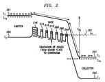
- Fig. 2 is a representation of the relative conduction and valance band energies present in the phototransistor of Fig. 1 when the transistor is properly biased.
- The long wavelength infrared photodetector constructed in accordance with the present invention is essentially an npn transistor in which the base region consists of a quantum well structure constructed of alternating layers of silicon germanium (Si1-xGex) and silicon (Si). These alternating layers of SiGe and Si provide a sequence of quantum wells primarily in the valance band as described hereinafter in connection with Fig. 2. As shown in Fig. 1, the phototransistor is fabricated by first growing an approximately 1 µm (micrometer)
thick Si layer 101 with n-type doping on a highlyresistive Si substrate 100 to form the collector region of the phototransistor. Thislayer 101 is n-doped at a level of about 2 X 10¹⁸ cm⁻³ for the first 0.5 µm of growth and at a level of about 1 X 10¹⁶ cm⁻³ in the remaining 0.5 µm. Next aSi layer 103 with a p-type doping level of about 5 X 10¹⁷ cm⁻³ is grown to a thickness of about 300 Å ontolayer 101.Layer 103 is p-doped in order to reduce the leakage current of the base-collector junction. Then a p-doped Si1-xGex layer 104 is grown with a thickness of about 40 Å onlayer 103 followed by anundoped Si layer 105. This process of alternately growing layers of Si1-xGex followed by layers of undoped Si is then repeated to form layers 106-115 in Fig. 1. All of the undoped Si layers are grown with a thickness of about 300 Å, and the Si1-xGex layers described thus far are grown with thicknesses of about 40 Å and p-doped with levels of about 2 X 10¹⁸ cm⁻³, where the germanium mole fractions (x) are about 20 percent. - It should be noted that
layer 103 may be eliminated, andlayer 104 can be grown directly oncollector layer 101 without departing from the spirit and scope of the present invention. Sincelayer 104 is also p-doped, it will also function so as to reduce the leakage current of the base-collector junction. - The final Si1-xGex
layer 116 is grown onlayer 115 and is also p-doped to a level of about 2 X 10¹⁸ cm⁻³, but it is grown with a larger thickness of about 60 Å and a larger germanium mole fraction (x) of about 25 percent in order to provide a wider and deeper quantum well in the valance band than the quantum wells provided by the even-numberedlayers 104 through 114. The effect of this wider and deeper quantum well will be more apparent after the discussion hereinafter in connection with Fig. 2. - Finally an n-doped
layer 117 is grown onlayer 116 to form the emitter region with n-type doping levels of about 2 X 10¹⁷ cm⁻³. The entire grown structure is then masked and etched so as to expose thecollector layer 101 onto which ametallic contact 102 is deposited in order to provide a connection to the collector region. Ametallic contact 118 is also deposited onlayer 117 in order to provide a connection to the emitter region. Bothlayers layers 103 through 116, and therefor only segments oflayers - To bias and operate the phototransistor, an
external power source 120 in Fig. 1 has its positive terminal directly connected to contact 102 and its negative terminal connected through aload impedance 119 to thecontact 118. The infrared light beam to be detected, shown as 125 in Fig. 1, is coupled through the back ofsubstrate 100 passing through the collector region into the base region which consists oflayers 103 through 116. With the bias as indicated, the lower energy level of the conduction band, EC, and the upper energy level of the valance band, EV, are as shown in Fig. 2 bycurves - As further indicated in Fig. 2, the
infrared light beam 125 is coupled through the collector region (layer 101) and through absorption excites a hole from a bound state in a SiGe quantum well either to a higher state within the well or to the continuum above the barriers provided by the odd-numbered Si layers 103-115. The quantum wells of Fig. 2 are designated by numbers which are identical to the layers which produce them except that the hundreds digit has been changed from one hundred in Fig. 1 to two hundred in fig. 2. For example, the quantum well produced bylayer 116 in Fig. 1 is designated asquantum well 216 in Fig. 2 and is shown as being wider and deeper than the other quantum wells. As a result, the holes which are excited drift and/or tunnel to the base-emitter junction and accumulate inquantum well 216 due to the large potential barrier in the valance band. To neutralize the accumulated holes, a large injection of electrons occurs from the emitter into the base region thereby resulting in a large current flow from the emitter to the collector which in turn results in larger current and optical gains. This increase in current flow resulting fromlight beam 125 produces an output signal in the form of a change in the potential drop acrossload impedance 119 of Fig. 1. - The device described hereinabove operates in a two-terminal mode. The holes lost due to recombination with minority carrier electrons will largely be replaced by injection of holes from the collector and by thermal generation in the base-collector depletion region. The most efficient method of replacing the lost holes would, however, be a small continuous wave or pulsed light bias whose wavelength should match the bandgap of the SiGe quantum well. Such a light bias will make the device equivalent to a three terminal device.
- Any hole transfer from any quantum well to the quantum well next to the emitter-base junction would increase the forward bias, VBE, resulting in an increased electron injection and thus increased current flow. If the emitter efficiency is close to unity, the current gain, β, is the ratio of the electron lifetime, τT, and the electron transit time, τt, in the base:

Because of the diffusion and drift field in the base, the transit time is expected to be very small. If the quantum efficiency is η, the optical gain, g, will be as follows:
The carrier multiplication in the base-collection depletion region can further increase the optical gain in accordance with the following equation:
where M is the avalanche multiplication factor. If M in the last equation is slightly greater than unity, there will be a marked increase in current and optical gains. Note that this carrier multiplication also increases the dark current that will, however, not matter much if the dark current is much smaller than the photocurrent. - In the device described hereinabove, the holes are excited but the current transport in the base is through the electrons which occurs both by diffusion and drift. The device has a reversed biased p/n junction between the base and collector regions which causes the amount of leakage current to be much smaller than prior art quantum well devices which have no p/n junctions. The proposed device is accordingly expected to operate at relatively higher temperatures. Because the proposed photodetector has gain, the associated electronics can be reduced significantly. Furthermore, since the proposed photodetector is based on a silicon materials system, silicon electronics can be placed on the same substrate thereby resulting in less complex and more reliable circuits.
Claims (9)
- A phototransistor comprising emitter, base, collector regions, said emitter and collector regions being doped such that they are of the same conductivity type, said base region being doped such that it is the opposite conductivity type, and means for conductively coupling to said emitter and collector regions such that an output signal can be developed in response to an external light beam impinging on said phototransistor, characterized in that said base region comprises multiple layers of semiconductor material in a quantum well structure, the material in each layer being chosen such that the bandgap between its valance and conduction bands is different from the bandgap in adjacent layers whereby quantum wells are created in said base region.
- A phototransistor as defined in claim 1 wherein said material in each layer is chosen such that there is no substantial discontinuity in the conduction band between adjacent layers and the difference in bandgap between adjacent layers primarily causes discontinuities in the valance bands, whereby the quantum wells are primarily in the valance band.
- A phototransistor as defined in claim 2 wherein the emitter and collector regions are n-doped silicon, and the multiple layers of said base region alternate between undoped silicon and p-doped SiGe.
- A phototransistor as defined in claim 3 wherein the SiGe layer adjacent to said emitter region is thicker than the other SiGe layers in said base region and also has a higher percentage of germanium than the other SiGe layers, whereby the quantum well closest to said emitter layer is wider and deeper than the other quantum wells in said base region.
- A phototransistor as defined in claims 3 or 4 wherein said base region further includes a p-doped silicon layer adjacent to said collector region.
- A photodetector for developing an output signal in response to an external light beam, said photodetector comprising multiple layers of semiconductor material arranged to form a quantum well structure having a first layer and a last layer, the material of said multiple layers being chosen such that each layer has a bandgap between its valance and conduction bands different from the bandgap of adjacent layers thereby forming quantum wells in alternate layers with barrier layers between, said barrier layers being undoped and the alternate layers having the quantum wells being doped such that they are all of a first conductivity type, first means for conductively coupling to said first layer, and a second means for conductively coupling to said last layer, said output signal appearing between said first and second coupling means when said light beam impinges on said multiple layers, characterized in that said first and second coupling means includes semiconductor material having a dopant such that they are both of a conductivity type opposite to said first conductivity type.
- A photodetector as defined in claim 6 wherein said last layer of said quantum well structure is a layer having a quantum well, said last layer being thicker and having a smaller bandgap than the other layers having quantum wells.
- A photodetector as defined in claims 6 or 7 wherein said first layer is a barrier layer and said first layer is doped such that it is said first conductivity type.
- A photodetector as defined in claims 6, 7, or 8 wherein said quantum well structure includes alternating layers of p-doped silicon germanium and undoped silicon, and said first and second coupling means each include n-doped silicon.
Applications Claiming Priority (2)
| Application Number | Priority Date | Filing Date | Title |
|---|---|---|---|
| US08/104,969 US5399880A (en) | 1993-08-10 | 1993-08-10 | Phototransistor with quantum well base structure |
| US104969 | 1993-08-10 |
Publications (2)
| Publication Number | Publication Date |
|---|---|
| EP0638941A2 true EP0638941A2 (en) | 1995-02-15 |
| EP0638941A3 EP0638941A3 (en) | 1996-12-18 |
Family
ID=22303418
Family Applications (1)
| Application Number | Title | Priority Date | Filing Date |
|---|---|---|---|
| EP94305747A Withdrawn EP0638941A3 (en) | 1993-08-10 | 1994-08-03 | Phototransistor with a basic quantum well structure. |
Country Status (2)
| Country | Link |
|---|---|
| US (1) | US5399880A (en) |
| EP (1) | EP0638941A3 (en) |
Cited By (4)
| Publication number | Priority date | Publication date | Assignee | Title |
|---|---|---|---|---|
| US5844253A (en) * | 1996-11-22 | 1998-12-01 | Electronics And Telecommunications Research Institute | High speed semiconductor phototransistor |
| US5977557A (en) * | 1997-12-23 | 1999-11-02 | Electronics & Telecommunications Research Institute | Hot-electron photo transistor |
| WO2006015280A3 (en) * | 2004-07-28 | 2006-05-18 | Massachusetts Inst Technology | Photodetectors including germanium |
| CN105116038A (en) * | 2015-07-20 | 2015-12-02 | 深圳大学 | Organic semiconductor based immunodetection integrated chip and preparation method thereof |
Families Citing this family (28)
| Publication number | Priority date | Publication date | Assignee | Title |
|---|---|---|---|---|
| KR19980041071A (en) * | 1996-11-30 | 1998-08-17 | 구자홍 | Heterojunction Bipolar Transistor |
| US6137123A (en) * | 1999-08-17 | 2000-10-24 | Honeywell International Inc. | High gain GaN/AlGaN heterojunction phototransistor |
| US6346431B1 (en) * | 2000-07-10 | 2002-02-12 | Lg Electronics Inc. | Quantum dot infrared detection device and method for fabricating the same |
| US6980748B2 (en) * | 2001-08-30 | 2005-12-27 | International Business Machines Corporation | SiGe or germanium flip chip optical receiver |
| ATE365382T1 (en) * | 2002-11-29 | 2007-07-15 | Max Planck Gesellschaft | SEMICONDUCTOR STRUCTURE FOR INFRARED RANGE AND PRODUCTION PROCESS |
| US7696536B1 (en) * | 2003-08-22 | 2010-04-13 | The Board Of Trustees Of The University Of Illinois | Semiconductor method and device |
| US7091082B2 (en) | 2003-08-22 | 2006-08-15 | The Board Of Trustees Of The University Of Illinois | Semiconductor method and device |
| US7998807B2 (en) * | 2003-08-22 | 2011-08-16 | The Board Of Trustees Of The University Of Illinois | Method for increasing the speed of a light emitting biopolar transistor device |
| US7286583B2 (en) | 2003-08-22 | 2007-10-23 | The Board Of Trustees Of The University Of Illinois | Semiconductor laser devices and methods |
| US20050040432A1 (en) * | 2003-08-22 | 2005-02-24 | The Board Of Trustees Of The University Of Illinois | Light emitting device and method |
| US7354780B2 (en) | 2003-08-22 | 2008-04-08 | The Board Of Trustees Of The University Of Illinois | Semiconductor light emitting devices and methods |
| US7535034B2 (en) * | 2006-02-27 | 2009-05-19 | The Board Of Trustees Of The University Of Illinois | PNP light emitting transistor and method |
| US7711015B2 (en) * | 2007-04-02 | 2010-05-04 | The Board Of Trustees Of The University Of Illinois | Method for controlling operation of light emitting transistors and laser transistors |
| US7923801B2 (en) | 2007-04-18 | 2011-04-12 | Invisage Technologies, Inc. | Materials, systems and methods for optoelectronic devices |
| US8525287B2 (en) | 2007-04-18 | 2013-09-03 | Invisage Technologies, Inc. | Materials, systems and methods for optoelectronic devices |
| US20100044676A1 (en) | 2008-04-18 | 2010-02-25 | Invisage Technologies, Inc. | Photodetectors and Photovoltaics Based on Semiconductor Nanocrystals |
| US7846806B1 (en) * | 2007-05-25 | 2010-12-07 | National Semiconductor Corporation | System and method for providing a self aligned silicon germanium (SiGe) heterojunction bipolar transistor using a mesa emitter-base architecture |
| WO2009058580A1 (en) * | 2007-10-31 | 2009-05-07 | Bae Systems Information And Electronic Systems Integration Inc. | High-injection heterojunction bipolar transistor |
| US8138567B2 (en) * | 2008-04-18 | 2012-03-20 | Invisage Technologies, Inc. | Materials, fabrication equipment, and methods for stable, sensitive photodetectors and image sensors made therefrom |
| US8203195B2 (en) | 2008-04-18 | 2012-06-19 | Invisage Technologies, Inc. | Materials, fabrication equipment, and methods for stable, sensitive photodetectors and image sensors made therefrom |
| CN102165572B (en) * | 2008-07-21 | 2013-12-25 | 因维奇技术公司 | Materials, fabrication equipment, and methods for stable, sensitive photodetectors and image sensors made therefrom |
| WO2011156507A1 (en) | 2010-06-08 | 2011-12-15 | Edward Hartley Sargent | Stable, sensitive photodetectors and image sensors including circuits, processes, and materials for enhanced imaging performance |
| US9548408B2 (en) | 2014-04-15 | 2017-01-17 | L-3 Communications Cincinnati Electronics Corporation | Tunneling barrier infrared detector devices |
| CN108039363A (en) * | 2017-11-30 | 2018-05-15 | 电子科技大学 | Optical drive SiC/GaN based semiconductor devices and its manufacture craft |
| JP6909165B2 (en) * | 2018-01-15 | 2021-07-28 | 富士通株式会社 | Manufacturing method of infrared detector, image sensor, imaging system, infrared detector |
| US10680086B2 (en) * | 2018-06-18 | 2020-06-09 | Qualcomm Incorporated | Radio frequency silicon-on-insulator integrated heterojunction bipolar transistor |
| US11011666B2 (en) * | 2018-08-15 | 2021-05-18 | National Taiwan University Of Science And Technology | Optoelectronic semiconductor structure having a bipolar phototransistor structure and manufacturing method thereof |
| CN121368218B (en) * | 2025-12-19 | 2026-04-21 | 厦门银科启瑞半导体科技有限公司 | Anti-irradiation solar cell |
Family Cites Families (3)
| Publication number | Priority date | Publication date | Assignee | Title |
|---|---|---|---|---|
| US4160258A (en) * | 1977-11-18 | 1979-07-03 | Bell Telephone Laboratories, Incorporated | Optically coupled linear bilateral transistor |
| JPS63140570A (en) * | 1986-12-03 | 1988-06-13 | Hitachi Ltd | Semiconductor device |
| US5077593A (en) * | 1989-12-27 | 1991-12-31 | Hughes Aircraft Company | Dark current-free multiquantum well superlattice infrared detector |
-
1993
- 1993-08-10 US US08/104,969 patent/US5399880A/en not_active Expired - Lifetime
-
1994
- 1994-08-03 EP EP94305747A patent/EP0638941A3/en not_active Withdrawn
Non-Patent Citations (5)
| Title |
|---|
| APPLIED PHYSICS LETTERS, vol. 52, no. 13, 28 March 1988, pages 1089-1091, XP000112114 TEMKIN H ET AL: "GEXSI1-X STRAINED-LAYER HETEROSTRUCTURE BIPOLAR TRANSISTORS" * |
| APPLIED PHYSICS LETTERS, vol. 59, no. 20, 11 November 1991, pages 2588-2590, XP000330117 KARUNASIRI R P G ET AL: "SI1-XGEX/SI MULTIPLE QUANTUM WELL INFRARED DETECTOR" * |
| CHAND N ET AL: "Gain of a heterojunction bipolar phototransistor" , IEEE TRANSACTIONS ON ELECTRON DEVICES, MARCH 1985, USA, VOL. ED-32, NR. 3, PAGE(S) 622 - 627 , ISSN 0018-9383 XP002016090 * page 625, paragraph 3B; figure 1 * * |
| ELECTRONICS LETTERS, vol. 29, no. 20, 30 September 1993, pages 1800-1802, XP000400441 CHAND N: "LWIP: A LONG-WAVELENGTH INFRA-RED PHOTOTRANSISTOR" * |
| IEE PROCEEDINGS J. OPTOELECTRONICS, vol. 138, no. 3 PART J, 1 June 1991, pages 226-234, XP000238660 CHANG C Y ET AL: "AMORPHOUS SI/SIC PHOTOTRANSISTORS AND AVALANCHE PHOTODIODES" * |
Cited By (6)
| Publication number | Priority date | Publication date | Assignee | Title |
|---|---|---|---|---|
| US5844253A (en) * | 1996-11-22 | 1998-12-01 | Electronics And Telecommunications Research Institute | High speed semiconductor phototransistor |
| US5977557A (en) * | 1997-12-23 | 1999-11-02 | Electronics & Telecommunications Research Institute | Hot-electron photo transistor |
| WO2006015280A3 (en) * | 2004-07-28 | 2006-05-18 | Massachusetts Inst Technology | Photodetectors including germanium |
| US7723754B2 (en) | 2004-07-28 | 2010-05-25 | Massachusetts Institute Of Technology | Ge photodetectors |
| CN105116038A (en) * | 2015-07-20 | 2015-12-02 | 深圳大学 | Organic semiconductor based immunodetection integrated chip and preparation method thereof |
| CN105116038B (en) * | 2015-07-20 | 2018-06-29 | 深圳大学 | One kind is based on organic semi-conductor immune detection integrated chip and preparation method thereof |
Also Published As
| Publication number | Publication date |
|---|---|
| EP0638941A3 (en) | 1996-12-18 |
| US5399880A (en) | 1995-03-21 |
Similar Documents
| Publication | Publication Date | Title |
|---|---|---|
| US5399880A (en) | Phototransistor with quantum well base structure | |
| US5077593A (en) | Dark current-free multiquantum well superlattice infrared detector | |
| US6326654B1 (en) | Hybrid ultraviolet detector | |
| US4894526A (en) | Infrared-radiation detector device | |
| US4015280A (en) | Multi-layer semiconductor photovoltaic device | |
| Decoster et al. | Optoelectronic sensors | |
| EP0167305B1 (en) | Photodetector | |
| US4679061A (en) | Superlattice photoconductor | |
| US5198682A (en) | Multiple quantum well superlattice infrared detector with graded conductive band | |
| US5563423A (en) | Dark current-free multiquantum well superlattice infrared detector | |
| Capasso | New multilayer and graded gap optoelectronic and high speed devices by band gap engineering | |
| KR920009918B1 (en) | Quantum-well radiation detector | |
| EP0444963A2 (en) | Photoelectric transfer device | |
| US4525731A (en) | Semiconductor conversion of optical-to-electrical energy | |
| US4282541A (en) | Planar P-I-N photodetectors | |
| CN112447875A (en) | Avalanche type photoelectric transistor element and its optical detection method | |
| EP0571944A1 (en) | Photoelectric conversion device | |
| US5260560A (en) | Photoelectric transfer device | |
| EP0495414A1 (en) | Photoelectric converting device and image processing apparatus utilizing the same | |
| GB1597538A (en) | Photovoltaic semiconductor device having increased detectivity and decreased capacitance | |
| Shen et al. | Effect of emitter layer concentration on the performance of GaAs p/sup+/-i homojunction far-infrared detectors: a comparison of theory and experiment | |
| JPS6244867B2 (en) | ||
| US5747864A (en) | Light receiving element and a method of fabricating the same | |
| EP0149178A2 (en) | Infrared detector system based on III-V epitaxial material | |
| De Cesare et al. | Modeling and realization of a high-gain homojunction a-Si: H bulk barrier phototransistor |
Legal Events
| Date | Code | Title | Description |
|---|---|---|---|
| PUAI | Public reference made under article 153(3) epc to a published international application that has entered the european phase |
Free format text: ORIGINAL CODE: 0009012 |
|
| AK | Designated contracting states |
Kind code of ref document: A2 Designated state(s): DE FR GB IT |
|
| PUAL | Search report despatched |
Free format text: ORIGINAL CODE: 0009013 |
|
| AK | Designated contracting states |
Kind code of ref document: A3 Designated state(s): DE FR GB IT |
|
| 17P | Request for examination filed |
Effective date: 19970604 |
|
| 17Q | First examination report despatched |
Effective date: 19971210 |
|
| STAA | Information on the status of an ep patent application or granted ep patent |
Free format text: STATUS: THE APPLICATION IS DEEMED TO BE WITHDRAWN |
|
| 18D | Application deemed to be withdrawn |
Effective date: 19980421 |