EP0637121A1 - Power converter assembly for the supply of an intermediate DC circuit - Google Patents
Power converter assembly for the supply of an intermediate DC circuit Download PDFInfo
- Publication number
- EP0637121A1 EP0637121A1 EP94111470A EP94111470A EP0637121A1 EP 0637121 A1 EP0637121 A1 EP 0637121A1 EP 94111470 A EP94111470 A EP 94111470A EP 94111470 A EP94111470 A EP 94111470A EP 0637121 A1 EP0637121 A1 EP 0637121A1
- Authority
- EP
- European Patent Office
- Prior art keywords
- connection
- diode
- semiconductor switch
- parallel
- circuit
- Prior art date
- Legal status (The legal status is an assumption and is not a legal conclusion. Google has not performed a legal analysis and makes no representation as to the accuracy of the status listed.)
- Granted
Links
Images


Classifications
-
- B—PERFORMING OPERATIONS; TRANSPORTING
- B60—VEHICLES IN GENERAL
- B60L—PROPULSION OF ELECTRICALLY-PROPELLED VEHICLES; SUPPLYING ELECTRIC POWER FOR AUXILIARY EQUIPMENT OF ELECTRICALLY-PROPELLED VEHICLES; ELECTRODYNAMIC BRAKE SYSTEMS FOR VEHICLES IN GENERAL; MAGNETIC SUSPENSION OR LEVITATION FOR VEHICLES; MONITORING OPERATING VARIABLES OF ELECTRICALLY-PROPELLED VEHICLES; ELECTRIC SAFETY DEVICES FOR ELECTRICALLY-PROPELLED VEHICLES
- B60L9/00—Electric propulsion with power supply external to the vehicle
- B60L9/16—Electric propulsion with power supply external to the vehicle using ac induction motors
- B60L9/30—Electric propulsion with power supply external to the vehicle using ac induction motors fed from different kinds of power-supply lines
-
- B—PERFORMING OPERATIONS; TRANSPORTING
- B60—VEHICLES IN GENERAL
- B60L—PROPULSION OF ELECTRICALLY-PROPELLED VEHICLES; SUPPLYING ELECTRIC POWER FOR AUXILIARY EQUIPMENT OF ELECTRICALLY-PROPELLED VEHICLES; ELECTRODYNAMIC BRAKE SYSTEMS FOR VEHICLES IN GENERAL; MAGNETIC SUSPENSION OR LEVITATION FOR VEHICLES; MONITORING OPERATING VARIABLES OF ELECTRICALLY-PROPELLED VEHICLES; ELECTRIC SAFETY DEVICES FOR ELECTRICALLY-PROPELLED VEHICLES
- B60L9/00—Electric propulsion with power supply external to the vehicle
- B60L9/16—Electric propulsion with power supply external to the vehicle using ac induction motors
- B60L9/18—Electric propulsion with power supply external to the vehicle using ac induction motors fed from dc supply lines
- B60L9/22—Electric propulsion with power supply external to the vehicle using ac induction motors fed from dc supply lines polyphase motors
-
- G—PHYSICS
- G05—CONTROLLING; REGULATING
- G05F—SYSTEMS FOR REGULATING ELECTRIC OR MAGNETIC VARIABLES
- G05F3/00—Non-retroactive systems for regulating electric variables by using an uncontrolled element, or an uncontrolled combination of elements, such element or such combination having self-regulating properties
- G05F3/02—Regulating voltage or current
- G05F3/08—Regulating voltage or current wherein the variable is dc
- G05F3/10—Regulating voltage or current wherein the variable is dc using uncontrolled devices with non-linear characteristics
- G05F3/16—Regulating voltage or current wherein the variable is dc using uncontrolled devices with non-linear characteristics being semiconductor devices
-
- H—ELECTRICITY
- H02—GENERATION; CONVERSION OR DISTRIBUTION OF ELECTRIC POWER
- H02M—APPARATUS FOR CONVERSION BETWEEN AC AND AC, BETWEEN AC AND DC, OR BETWEEN DC AND DC, AND FOR USE WITH MAINS OR SIMILAR POWER SUPPLY SYSTEMS; CONVERSION OF DC OR AC INPUT POWER INTO SURGE OUTPUT POWER; CONTROL OR REGULATION THEREOF
- H02M5/00—Conversion of ac power input into ac power output, e.g. for change of voltage, for change of frequency, for change of number of phases
- H02M5/40—Conversion of ac power input into ac power output, e.g. for change of voltage, for change of frequency, for change of number of phases with intermediate conversion into dc
- H02M5/42—Conversion of ac power input into ac power output, e.g. for change of voltage, for change of frequency, for change of number of phases with intermediate conversion into dc by static converters
- H02M5/44—Conversion of ac power input into ac power output, e.g. for change of voltage, for change of frequency, for change of number of phases with intermediate conversion into dc by static converters using discharge tubes or semiconductor devices to convert the intermediate dc into ac
- H02M5/443—Conversion of ac power input into ac power output, e.g. for change of voltage, for change of frequency, for change of number of phases with intermediate conversion into dc by static converters using discharge tubes or semiconductor devices to convert the intermediate dc into ac using devices of a thyratron or thyristor type requiring extinguishing means
- H02M5/45—Conversion of ac power input into ac power output, e.g. for change of voltage, for change of frequency, for change of number of phases with intermediate conversion into dc by static converters using discharge tubes or semiconductor devices to convert the intermediate dc into ac using devices of a thyratron or thyristor type requiring extinguishing means using semiconductor devices only
- H02M5/4505—Conversion of ac power input into ac power output, e.g. for change of voltage, for change of frequency, for change of number of phases with intermediate conversion into dc by static converters using discharge tubes or semiconductor devices to convert the intermediate dc into ac using devices of a thyratron or thyristor type requiring extinguishing means using semiconductor devices only having a rectifier with controlled elements
-
- H—ELECTRICITY
- H02—GENERATION; CONVERSION OR DISTRIBUTION OF ELECTRIC POWER
- H02M—APPARATUS FOR CONVERSION BETWEEN AC AND AC, BETWEEN AC AND DC, OR BETWEEN DC AND DC, AND FOR USE WITH MAINS OR SIMILAR POWER SUPPLY SYSTEMS; CONVERSION OF DC OR AC INPUT POWER INTO SURGE OUTPUT POWER; CONTROL OR REGULATION THEREOF
- H02M7/00—Conversion of ac power input into dc power output; Conversion of dc power input into ac power output
- H02M7/02—Conversion of ac power input into dc power output without possibility of reversal
- H02M7/04—Conversion of ac power input into dc power output without possibility of reversal by static converters
- H02M7/12—Conversion of ac power input into dc power output without possibility of reversal by static converters using discharge tubes with control electrode or semiconductor devices with control electrode
- H02M7/145—Conversion of ac power input into dc power output without possibility of reversal by static converters using discharge tubes with control electrode or semiconductor devices with control electrode using devices of a thyratron or thyristor type requiring extinguishing means
- H02M7/155—Conversion of ac power input into dc power output without possibility of reversal by static converters using discharge tubes with control electrode or semiconductor devices with control electrode using devices of a thyratron or thyristor type requiring extinguishing means using semiconductor devices only
-
- B—PERFORMING OPERATIONS; TRANSPORTING
- B60—VEHICLES IN GENERAL
- B60L—PROPULSION OF ELECTRICALLY-PROPELLED VEHICLES; SUPPLYING ELECTRIC POWER FOR AUXILIARY EQUIPMENT OF ELECTRICALLY-PROPELLED VEHICLES; ELECTRODYNAMIC BRAKE SYSTEMS FOR VEHICLES IN GENERAL; MAGNETIC SUSPENSION OR LEVITATION FOR VEHICLES; MONITORING OPERATING VARIABLES OF ELECTRICALLY-PROPELLED VEHICLES; ELECTRIC SAFETY DEVICES FOR ELECTRICALLY-PROPELLED VEHICLES
- B60L2200/00—Type of vehicles
- B60L2200/26—Rail vehicles
Definitions
- the invention relates to a converter circuit for feeding a DC voltage intermediate circuit according to the preamble of claim 1 and is preferably used for three-phase track vehicles on 3kV direct current wire, but also for multi-system vehicles on direct current / alternating current contact wire.
- the circuits listed above for feeding three-phase consumers on the 3kV direct current wire can be divided into two main groups:
- the first main group concerns pulse inverters via an input filter directly on the DC contact wire: for example according to ETR ....
- Figure 4b series connection of two two-point inverters
- Figure 7 three-point inverters
- the second main group relates to pulse inverters with stabilized intermediate circuit voltage, which are fed via an input filter and DC chopper.
- ETR .... Fig. 5 Electric Railways .... Fig. 6 and ZEV + DET ... Fig. 5
- step-down converter circuits as well as step-up converter circuits are used.
- circuits mentioned above are suitable for supplying three-phase consumers from both the direct current contact wire and for supplying from a single-phase alternating current contact wire.
- the inverter is complex (ETR .... Fig. 7 and 4b). Since the DC voltage network fluctuates over a wide voltage range, the complete converter must be designed for the maximum voltage that occurs.
- the input filter capacity is essentially required to meet the network requirements with regard to low input resonance frequency, minimum input impedance, special network feedback requirements and to provide the DC chopper pulse power.
- the DC link capacitance is necessary to supply the commutation, distortion and displacement reactive power of inverters and consumers, as well as to absorb the DC power supply pulse power.
- the separate capacities require separate detectors and protective devices.
- the invention has for its object to provide a simply constructed converter circuit for feeding a DC link of the type mentioned, with which a stabilized DC link voltage is generated from the tolerant contact wire voltage, via which one or more inverters can be fed with the appropriate consumers.
- the advantages that can be achieved with the invention are, in particular, that the line filter capacitance and DC link capacitance are reduced, since both capacities (input filter and DC link capacitance) are integrated and work together in the function in the input subcapacities.
- the regulated intermediate circuit and the inverter are grounded on one side and - depending on the circuit used - as well as the connected loads, the insulation against ground must only be dimensioned for the voltage at a partial input capacitance.
- the integration of brake actuators, which limit the voltage at the input subcapacities is possible through a simple circuit expansion with semiconductor switches (thyristors) that cannot be automatically deleted.
- the circuit can be used universally and can be modularly adapted to any power by connecting in parallel without losing any advantages.
- the circuit can be used for 3kV single-system operation, multi-system operation (direct and alternating current contact wire) with one inverter per system (group drive) or for single-axis supply (several inverters work in parallel on one system).
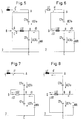
- FIG. 1a shows a single-quadrant DC chopper with energy transport from the network to the inverter.
- the contact wire 1 is connected via a filter choke LF to a connection point A, at which an automatically erasable semiconductor switch G1 and an input partial capacitance CFO are located.
- CFO is connected to a connection point B, at which an actuator choke LST, an input partial capacitance CFU and the positive DC connection of the inverter WR are located.
- G1 is connected to a connection point D, at which the further connection of LST and a diode D2 are located.
- CFU, D2 and the negative DC connection of WR are on the other hand via a connection point C on the wheel / rail system 2.
- WR is connected on the three-phase side (alternating connections) to a three-phase machine 3 (drive motor for rail vehicle).
- the voltage at CFO is UFO and the voltage at CFU is UFU.
- UFU UD
- FIG. 1b shows a two-quadrant DC chopper with energy transport in both directions.
- a diode D1 is parallel to G1 and an automatically erasable semiconductor switch G2 is parallel to D2.
- G1 is parallel to G1
- G2 is parallel to D2.
- FIG. 2a there is a single-quadrant DC chopper with energy transport from the network to the inverter for generation shown a higher DC link voltage.
- D1 lies between A and D and G2 lies between D and C.
- the positive DC connection of WR is connected to A.
- the contact wire 1 is connected to LF via LF.
- FIG. 2b shows a two-quadrant DC chopper with energy transport in both directions for a higher intermediate circuit voltage.
- G1 are parallel to D1 and D2 are parallel to G2. The rest of the arrangement is as described under Figure 2a.
- FIG. 3a shows a two-quadrant direct current controller (3-point controller circuit) with energy transport in both directions.
- the contact wire 1 is connected via LF to A of the basic arrangement CFO / CFU / LST and the positive DC connection of WR is connected to B.
- G1 / D1 is the parallel connection of a further automatically erasable semiconductor switch G3 with a diode D3 between A and D in series.
- G2, G4 in turn automatically erasable semiconductor switches and D2, D4 denote diodes.
- connection point labeled E between G1 / D1 and G3 / D3 is connected via a diode D5 and the connection point labeled F between G2 / D2 and G4 / D4 is connected to B via a diode D6.
- the direct current regulator according to FIG. 3a is suitable for high input voltages.
- FIG. 3b shows a two-quadrant DC chopper (also composed of three identical 2-point chopper circuits) that is also suitable for high input voltages and has energy transport in both directions.
- the automatically erasable semiconductor switches G5 and G6 are parallel to D5 and D6. The rest of the arrangement and the advantages are as described under Figure 3a.
- FIG. 4a shows a brake branch with semiconductor switches that cannot be automatically erased, as can be inserted in parallel with LST in all circuits between D and B as required.
- the braking branch consists of two anti-parallel semiconductor switches T1, T2 (thyristors) with a braking resistor RB arranged in series.
- FIG. 4b shows a brake branch with an automatically erasable semiconductor switch, as can be inserted in parallel with CFU in all circuits between B and C and in addition in parallel with CFO between A and B if necessary.
- the brake branch consists of an automatic Erasable semiconductor switch G7 with braking resistor RB in series.
- the input capacitance consists of the series connection of two capacitors CFO and CFU.
- the capacitance which is connected to ground on one side, is kept at a fixed, predetermined constant value by a DC control circuit and the control choke LST.
- UD UFU + UFO.
- the converter circuit can be an arrangement with a two-point circuit (see FIGS. 1a or 1b).
- the 3-point circuit shown in FIGS. 3a and 3b is suitable for higher voltages UFU + UFO.
- a 3-point circuit according to Figure 3b which is composed of three 2-point phases.
- this basic circuit can be regrouped by switching devices so that it works as an input actuator (4q-S) on the AC contact wire (see Figure 17).
- a braking resistor RB between the output of the DC chopper D and the division point B of the input capacitance, which can be switched on via non-automatically erasable semiconductors (thyristors) T1, T2 and thereby sets the ratio of the two partial voltages UFO and UFU.
- Separate brake branches according to FIG. 4b with automatically erasable semiconductors G7 can be connected in parallel to the capacitance CFU or to both capacitances CFU and CFO.
- DC regulator circuits with a corresponding smoothing inductor LST can be connected in parallel at points A, B and C.
- the DC controllers / 4q-S are connected in parallel at points A / B1 or B2 / C (see Figure 17).
- the additional transformer windings and converter chokes required for multi-system operation are connected to the input actuators connected in parallel via switching devices.
- the current over LF is iF
- the current over WR is iD
- the current over LST is iST.
- the inductance of LST is L.
- the energy is transported from the grid to the consumers via the inverter.
- the DC chopper works as a buck converter.
- a constant and smaller intermediate circuit voltage UD UFU is generated from the variable input voltage Unet. As shown in Figures 5 to 8, three switching states can be distinguished.
- G1 and G3 are conductive.
- the voltage UFO is at LST.
- the converter works as a step-up converter.
- LST is magnetized by UFU (switching state according to FIG. 8 with a changed current direction shown in dashed lines).
- the switch to the switching state according to FIG. 7 takes place (with the current direction drawn in dashed lines).
- the current iST can flow freely via G2 and D6.
- the switching state according to FIG. 6 is achieved by deleting G2 (with the direction of the current drawn in dashed lines), with a current flow via D3 and D1.
- a brake branch T1 / T2 / RB is connected in parallel with LST.
- the special feature of this braking branch is that it consists of one or two braking resistors (a braking resistor is assigned to each semiconductor switch T1, T2) and two semiconductors T1, T2 that cannot be automatically erased. These semiconductors that cannot be automatically erased are automatically erased when G1, G3 or D1, D3 (deletion of T2) or G2, G4 or D2, D4 (deletion of T1) become conductive.
- the advantage of this brake branch according to FIG. 4a is the low circuit complexity compared to one or two brake branches, which are equipped with automatically erasable semiconductor switches and monitoring devices and are arranged in parallel with the CFO or in parallel with the CFU (see FIG. 4b).
- the mode of operation of the brake branch according to FIG. 4a used in the circuit according to FIG. 3a is described below with reference to FIGS. 8 to 16.
- the current over RB is iRB.
- the current iST flows in the actuator choke LST according to the counting arrows. Ignition of G2 and G4 results in the equivalent image according to FIG. 8 with a changed current supply (indicated by dashed lines), the inductor LST is magnetized.
- T2 can be ignited simultaneously with G2 and G4 or delayed accordingly (see Figure 9).
- the total current iRB + iST flows via G2 and G4.
- the choke current iST flows in freewheeling via G2 and D6 without counter voltage.
- LRB are parasitic inductors or di / dt limiting chokes and R denotes the ohmic resistance value of RB.
- T1 as well as G1 and G3 can be switched on with a delay, so that the equivalent circuit diagram according to FIG. 13 is achieved.
- the circuit shown in FIG. 17 shows a multi-system-compatible basic circuit for operation on (in particular 3 kV) direct current contact wire and on single-phase alternating current contact wire and is based on the circuit according to FIG. 3 b.
- the Circuit is modified in that the connection between CFO and B can be separated by means of a first switching device S1 (B is split into B1, B2), the connection between C and the wheel / rail system 2 can be separated by means of a second switching device S2 of a third switching device S3 the connection between E and G3 / D3 can be disconnected, by means of a fourth switching device S4 the connection between F and G2 / D2 can be disconnected, by means of a fifth switching device S5 the connection between LST and D can be disconnected and by means of a sixth switching device S6 an additional suction circuit capacitor CSaug can be connected in parallel to the CFU.
- a first switching device S1 B is split into B1, B2
- the connection between C and the wheel / rail system 2 can be separated by
- the contact positions of the switching devices S1 ... S6 shown in Figure 17 show the grouping on the 3kV direct current wire.
- the contact wire 1 is connected to LF via a main switch 5 for direct current feeding.
- Another main switch 7 connected to the contact wire 1 for alternating current feed is opened.
- S1 ... S5 are switched in such a way that the circuit configuration according to FIG. 3b including the brake branch according to FIG. 4a results.
- S6 is closed to achieve the parallel connection of UFU and CSaug.
- the connection points B1, B2 are connected to one another via S1 and correspond to B according to FIG.
- a brake branch T1 / T2 / RB is arranged between B1 and D.
- one or two separate branches in accordance with FIG. 4b can be used as brake branches parallel to the CFU and / or CFO.
- the CFU and CFO are connected in parallel and together form the DC link capacity at which the inverter is located.
- the transformer secondary winding TR1 is connected to the AC inputs E and F.
- the suction circuit is tuned to twice the mains frequency and absorbs the pendulum power caused by the 4q-S input rectification G1 / D1, G5 / D5, G6 / D6, G4 / D4.
- the branch G3, T1, RB can be used as a braking branch on the AC contact wire.
- the circuit is designed so that as many components as possible can be used for both systems. If components are only required for one system, some switching devices, e.g. S3 and S6 are eliminated. Switchgear S3 can be omitted if the brake branch is not required for operation on the AC contact wire. G3, D3, one side of the transformer secondary winding TR1 and point E are then firmly connected.
- the parallel-connected DC choppers / 4q-S are connected directly to points A / B1 or B2 / C.
- the additional transformer secondary windings TR2 ... and actuator chokes are connected to the parallel connected input converters via separate switching devices S3 ', S4' and S5 '(not shown).
Abstract
Description
Die Erfindung bezieht sich auf eine Stromrichterschaltung zur Speisung eines Gleichspannungszwischenkreises gemäß dem Oberbegriff des Anspruchs 1 und dient vorzugsweise zur Anwendung bei Drehstromschienenfahrzeugen am 3kV Gleichstromfahrdraht, aber auch für Mehrsystemfahrzeuge am Gleichstrom/Wechselstromfahrdraht.The invention relates to a converter circuit for feeding a DC voltage intermediate circuit according to the preamble of
Schaltungen, die es ermöglichen, aus einem 3kV Gleichstromfahrdraht Drehstromverbraucher zu speisen, sind aus P. Appun und E. Reichelt "Mehrsystemlokomotiven - heutige technische Möglichkeiten der Realisierung" ETR 38 (1989), H. 4, Seite 195 bis 200, A. Fuchs "Die Antriebstechnik der S 252 der Spanischen Staatsbahnen RENFE", Elektrische Bahnen 11/91, Seite 378/62 bis 380/64 sowie aus M. Eisele "Die Zweikraft-Lokomotiven C 38 mit Drehstrom-Antriebstechnik für die Südafrikanischen Eisenbahnen Spoornet" ZEV+DET Glasers Analen 117 (1993) Nr. 2/3, Seite 70 bis 78 bekannt.Circuits that make it possible to feed three-phase consumers from a 3kV direct current wire are from P. Appun and E. Reichelt "Multi-system locomotives - today's technical possibilities of implementation" ETR 38 (1989), H. 4, pages 195 to 200, A. Fuchs "The drive technology of the S 252 of the Spanish State Railways RENFE",
Die vorstehend aufgeführten Schaltungen zur Speisung von Drehstromverbrauchern am 3kV Gleichstromfahrdraht lassen sich in zwei Hauptgruppen aufteilen:
Die erste Hauptgruppe betrifft Pulswechselrichter über ein Eingangsfilter direkt am Gleichstromfahrdraht: beispielsweise nach ETR.... Bild 4b (Reihenschaltung von zwei Zweipunktwechselrichtern) und Bild 7 (Dreipunktwechselrichter).The circuits listed above for feeding three-phase consumers on the 3kV direct current wire can be divided into two main groups:
The first main group concerns pulse inverters via an input filter directly on the DC contact wire: for example according to ETR .... Figure 4b (series connection of two two-point inverters) and Figure 7 (three-point inverters).
Die zweite Hauptgruppe betrifft Pulswechselrichter mit stabilisierter Zwischenkreisspannung, die über ein Eingangsfilter und Gleichstromsteller gespeist werden. Wie in ETR.... Bild 5, Elektrische Bahnen.... Bild 6 und ZEV+DET... Bild 5 gezeigt, werden sowohl Tiefsetzstellerschaltungen als auch Hochsetzstellerschaltungen verwendet.The second main group relates to pulse inverters with stabilized intermediate circuit voltage, which are fed via an input filter and DC chopper. As shown in ETR .... Fig. 5, Electric Railways .... Fig. 6 and ZEV + DET ... Fig. 5, step-down converter circuits as well as step-up converter circuits are used.
Die vorstehend angeführten Schaltungen eignen sich zur Speisung von Drehstromverbrauchern sowohl aus dem Gleichstromfahrdraht als auch zur Speisung aus einem einphasigen Wechselstromfahrdraht.The circuits mentioned above are suitable for supplying three-phase consumers from both the direct current contact wire and for supplying from a single-phase alternating current contact wire.
Die Nachteile der Anordnungen gemäß erster Hauptgruppe bestehen in folgenden Punkten:
Der Wechselrichter ist aufwendig (ETR.... Bild 7 und 4b). Da das Gleichspannungsnetz im weiten Spannungsbereich schwankt, muß der komplette Umrichter für die maximal auftretende Spannung ausgelegt sein.The disadvantages of the arrangements according to the first main group consist in the following points:
The inverter is complex (ETR .... Fig. 7 and 4b). Since the DC voltage network fluctuates over a wide voltage range, the complete converter must be designed for the maximum voltage that occurs.
Die Maschinen sind aufwendiger wegen notwendiger erhöhter Isolation und bei ETR.... Bild 4b zusätzlich wegen der speziellen Wicklungen.The machines are more complex because of the increased insulation required and with ETR .... Figure 4b also because of the special windings.
Die Speisung von Kleinverbrauchern durch separate Stromrichter ist mit hohem Aufwand verbunden, da diese Stromrichter auch für die extremen Netzspannungstoleranzen zu dimensionieren sind.The feeding of small consumers by separate converters is associated with great effort, since these converters must also be dimensioned for the extreme mains voltage tolerances.
Die aktive Unterdrückung der durch den Pulswechselrichter hervorgerufenen störenden Netzstromoberschwingungen durch einen Gleichstromsteller ist nicht möglich.Active suppression of the disturbing mains current harmonics caused by the pulse inverter is not possible by means of a DC chopper.
Die Nachteile der Anordnungen gemäß zweiter Hauptgruppe (mit Vorsteller) bestehen in folgenden Punkten:
Je nach Schaltung müssen auch der Wechselrichter und die Maschinen für die maximal auftretende Netzspannung isoliert werden (bei ETR... Bild 5 nicht).The disadvantages of the arrangements according to the second main group (with introducer) are as follows:
Depending on the circuit, the inverter and the machines must also be isolated for the maximum grid voltage that occurs (not with ETR ... Fig. 5).
Es müssen sowohl eine eigene Eingangsfilterkapazität als auch eine eigene Zwischenkreiskapazität installiert werden (siehe ETR.... Bild 5, Elektrische Bahnen.... Bild 4 und ZEV+DET....Bild 5). Die Eingangsfilterkapazität ist im wesentlichen zur Erfüllung der Netzanforderung hinsichtlich niedriger Eingangsresonanzfrequenz, Mindesteingangsimpedanz, spezieller Netzrückwirkungsforderungen und zur Bereitstellung der Gleichstromstellerpulsleistung erforderlich. Die Zwischenkreiskapazität ist zur Lieferung der Kommutierungs-, Verzerrungs- und Verschiebungsblindleistung von Wechselrichtern und Verbrauchern, sowie zur Aufnahme der Gleichstromstellerpulsleistung notwendig.Both your own input filter capacity and your own DC link capacity must be installed (see ETR .... Fig. 5, Electrical Railways .... Fig. 4 and ZEV + DET .... Fig. 5). The input filter capacity is essentially required to meet the network requirements with regard to low input resonance frequency, minimum input impedance, special network feedback requirements and to provide the DC chopper pulse power. The DC link capacitance is necessary to supply the commutation, distortion and displacement reactive power of inverters and consumers, as well as to absorb the DC power supply pulse power.
Die getrennten Kapazitäten erfordern entsprechend separate Erfassungen und Schutzeinrichtungen.The separate capacities require separate detectors and protective devices.
Ein Teil der Schaltungen, wie z.B. die Schaltung in Elektrische Bahnen... ist nur attraktiv bei zwei Ausgangswechselrichtern.Part of the circuits, e.g. switching in electrical tracks ... is only attractive with two output inverters.
Der Erfindung liegt die Aufgabe zugrunde, eine einfach aufgebaute Stromrichterschaltung zur Speisung eines Gleichspannungszwischenkreises der eingangs genannten Art anzugeben, mit der aus der toleranzbehafteten Fahrdrahtspannung eine stabilisierte Zwischenkreisspannung erzeugt wird, über die ein oder mehrere Wechselrichter mit den entsprechenden Verbrauchern gespeist werden können.The invention has for its object to provide a simply constructed converter circuit for feeding a DC link of the type mentioned, with which a stabilized DC link voltage is generated from the tolerant contact wire voltage, via which one or more inverters can be fed with the appropriate consumers.
Diese Aufgabe wird in Verbindung mit den Merkmalen des Oberbegriffes erfindungsgemäß durch die im Kennzeichen des Anspruchs 1 angegebenen Merkmale gelöst.This object is achieved in connection with the features of the preamble according to the invention by the features specified in the characterizing part of
Die mit der Erfindung erzielbaren Vorteile bestehen insbesondere darin, daß der Netzfilterkapazitäts- und Zwischenkreiskapazitätsaufwand reduziert ist, da beide Kapazitäten (Eingangsfilter- und Zwischenkreiskapazität) in der Funktion in den Eingangsteilkapazitäten integriert sind und zusammenwirken. Der geregelte Zwischenkreis und der Wechselrichter liegen einseitig an Masse und sind - je nach verwendeter Schaltung - ebenso wie die angeschlossenen Verbraucher von der Isolation gegen Masse nur für die Spannung an einer Eingangsteilkapazität zu bemessen. Die Integration von Bremsstellern, die die Spannung an den Eingangsteilkapazitäten begrenzen, ist durch eine einfache Schaltungsergänzung mit nicht selbsttätig löschbaren Halbleiterschaltern (Thyristoren) möglich. Die Schaltung ist universell einsetzbar und läßt sich modular durch Parallelschaltung an beliebige Leistungen anpassen, ohne daß Vorteile verloren gehen. So ist die Schaltung für 3kV-Einsystembetrieb, Mehrsystembetrieb (Gleich- und Wechselstromfahrdraht) mit einem Wechselrichter pro Anlage (Gruppenantrieb) oder bei Einzelachsspeisung (mehrere Wechselrichter arbeiten parallel an einer Anlage) einsetzbar.The advantages that can be achieved with the invention are, in particular, that the line filter capacitance and DC link capacitance are reduced, since both capacities (input filter and DC link capacitance) are integrated and work together in the function in the input subcapacities. The regulated intermediate circuit and the inverter are grounded on one side and - depending on the circuit used - as well as the connected loads, the insulation against ground must only be dimensioned for the voltage at a partial input capacitance. The integration of brake actuators, which limit the voltage at the input subcapacities, is possible through a simple circuit expansion with semiconductor switches (thyristors) that cannot be automatically deleted. The circuit can be used universally and can be modularly adapted to any power by connecting in parallel without losing any advantages. The circuit can be used for 3kV single-system operation, multi-system operation (direct and alternating current contact wire) with one inverter per system (group drive) or for single-axis supply (several inverters work in parallel on one system).
Vorteilhafte Ausgestaltungen der Erfindung sind in den Unteransprüchen gekennzeichnet.Advantageous embodiments of the invention are characterized in the subclaims.
Weitere Vorteile sind der nachfolgenden Beschreibung entnehmbar.Further advantages can be found in the following description.
Die Erfindung wird nachstehend anhand der in der Zeichnung dargestellten Ausführungsformen erläutert. Es zeigen:
- Figur 1a
- einen Einquadranten-Gleichstromsteller (2-Punktstellerschaltung) mit Energietransport vom Netz zum Wechselrichter,
- Figur 1b
- einen Zweiquadranten-Gleichstromsteller (2-Punktstellerschaltung) mit Energietransport in beiden Richtungen,
- Figur 2a
- einen Einquadranten-Gleichstromsteller (2-Punktstellerschaltung) mit Energietransport vom Netz zum Wechselrichter für eine höhere Zwischenkreisspannung,
- Figur 2b
- einen Zweiquadranten-Gleichstromsteller (2-Punktstellerschaltung) mit Energietransport in beiden Richtungen für eine höhere Zwischenkreisspannung,
- Figur 3a
- einen Zweiquadranten-Gleichstromsteller (3-Punktstellerschaltung) mit Energietransport in beiden Richtungen,
- Figur 3b
- einen Zweiquadranten-Gleichstromsteller (zusammengesetzt aus drei gleichen 2-Punktstellerschaltungen) mit Energietransport in beiden Richtungen,
- Figur 4a
- einen Bremszweig mit nicht selbsttätig löschbaren Halbleiterschaltern,
- Figur 4b
- einen Bremszweig mit selbsttätig löschbarem Halbleiterschalter,
Figuren 5 bis 8- Ersatzschaltbilder für den Fahrbetrieb zur Erläuterung der Betriebsweise der Schaltung gemäß Figur 3a,
- Figuren 8 bis 16
- Ersatzschaltbilder für kombinierte Netz- und Widerstandsbremse zur Erläuterung der Funktionsweise des Bremszweiges gemäß Figur 4a,
- Figur 17
- eine Grundschaltung für Mehrsystembetrieb am (insbesondere 3kV) Gleich- und Wechselstromfahrdraht.
- Figure 1a
- a single quadrant DC chopper (2-point chopper circuit) with Energy transport from the grid to the inverter,
- Figure 1b
- a two-quadrant DC chopper (2-point chopper circuit) with energy transport in both directions,
- Figure 2a
- a single quadrant DC chopper (2-point chopper circuit) with energy transport from the grid to the inverter for a higher DC link voltage,
- Figure 2b
- a two-quadrant DC chopper (2-point chopper circuit) with energy transport in both directions for a higher DC link voltage,
- Figure 3a
- a two-quadrant DC chopper (3-point chopper circuit) with energy transport in both directions,
- Figure 3b
- a two-quadrant DC chopper (composed of three identical 2-point chopper circuits) with energy transport in both directions,
- Figure 4a
- a braking branch with semiconductor switches that cannot be automatically deleted,
- Figure 4b
- a brake arm with an automatically erasable semiconductor switch,
- Figures 5 to 8
- Equivalent circuit diagrams for driving operation to explain the mode of operation of the circuit according to FIG. 3a,
- Figures 8 to 16
- Equivalent circuit diagrams for combined mains and resistance brakes to explain the functioning of the brake branch according to FIG. 4a,
- Figure 17
- a basic circuit for multi-system operation on (in particular 3kV) direct and alternating current contact wire.
In Figur 1a ist ein Einquadranten-Gleichstromsteller mit Energietransport vom Netz zum Wechselrichter dargestellt. Die Netzspannung UNetz (= Fahrdrahtspannung = Eingangsspannung) liegt zwischen Fahrdraht 1 (allgemein: positiver Netzanschluß) und Rad/Schiene-System 2 (allgemein: negativer Netzanschluß, Masse) an. Der Fahrdraht 1 ist über eine Filterdrossel LF mit einem Anschlußpunkt A verbunden, an dem ein selbsttätig löschbarer Halbleiterschalter G1 und eine Eingangsteilkapazität CFO liegen. CFO ist andererseits mit einem Anschlußpunkt B verbunden, an dem eine Stellerdrossel LST, eine Eingangsteilkapazität CFU und der positive Gleichanschluß des Wechselrichters WR liegen. G1 ist andererseits mit einem Anschlußpunkt D verbunden, an dem der weitere Anschluß von LST sowie eine Diode D2 liegen. CFU, D2 und der negative Gleichanschluß von WR liegen andererseits über einem Anschlußpunkt C am Rad/Schiene-System 2. WR ist drehstromseitig (Wechselanschlüsse) mit einer Drehstrommaschine 3 (Antriebsmotor für Schienenfahrzeug) verbunden. Die Spannung an CFO beträgt UFO und die Spannung an CFU beträgt UFU.FIG. 1a shows a single-quadrant DC chopper with energy transport from the network to the inverter. The mains voltage UNet (= contact wire voltage = input voltage) is between contact wire 1 (general: positive mains connection) and wheel / rail system 2 (general: negative mains connection, ground). The
Der Gleichstromsteller gemäß Figur 1a wandelt die variable Netzspannung UNetz in eine konstante und kleinere Spannung UFU = UD um, wobei UD die Zwischenkreisspannung bezeichnet. Der geregelte Zwischenkreis und der Wechselrichter sind vorteilhaft hinsichtlich der Isolation gegen Masse nur für UFU = UD zu bemessen.The DC converter according to FIG. 1 a converts the variable mains voltage U mains into a constant and lower voltage UFU = UD, where UD denotes the intermediate circuit voltage. The regulated DC link and the inverter are advantageous in terms of insulation against ground only for UFU = UD.
In Figur 1b ist ein Zweiquadranten-Gleichstromsteller mit Energietransport in beiden Richtungen dargestellt. Zusätzlich zur Schaltung gemäß Figur 1a liegen eine Diode D1 parallel zu G1 sowie ein selbsttätig löschbarer Halbleiterschalter G2 parallel zu D2. Die übrige Anordnung und die Vorteile sind wie unter Figur 1a beschrieben.FIG. 1b shows a two-quadrant DC chopper with energy transport in both directions. In addition to the circuit according to FIG. 1a, a diode D1 is parallel to G1 and an automatically erasable semiconductor switch G2 is parallel to D2. The rest of the arrangement and the advantages are as described under Figure 1a.
In Figur 2a ist ein Einquadranten-Gleichstromsteller mit Energietransport vom Netz zum Wechselrichter zur Erzeugung einer höheren Zwischenkreisspannung dargestellt. Wie bei den Figuren 1a, 1b und bei allen weiteren Schaltungen gemäß den Figuren 2b, 3a, 3b, 17 ist wiederum die Grundanordnung einer Eingangsteilkapazität CFO zwischen A und B, einer Eingangsteilkapazität CFU zwischen B und C und einer Stellerdrossel LST zwischen B und D vorgesehen, wobei an C das Rad/Schiene-System 2 sowie der negative Gleichanschluß (Masseanschluß) des Wechselrichters WR liegen. Diese Grundanordnung CFO/CFU/LST und insbesondere die Aufteilung der Eingangskapazität in zwei reihengeschaltete Eingangsteilkapazitäten CFO, CFU, die die Funktionen einer Eingangsfilterkapazität und einer Zwischenkreiskapazität ausüben, ist tragendes Merkmal aller Anordnungen.In FIG. 2a there is a single-quadrant DC chopper with energy transport from the network to the inverter for generation shown a higher DC link voltage. As in FIGS. 1a, 1b and in all other circuits in accordance with FIGS. 2b, 3a, 3b, 17, the basic arrangement of an input partial capacitance CFO between A and B, an input partial capacitance CFU between B and C and an actuator choke LST between B and D is again provided , where the wheel /
Bei der Schaltung gemäß Figur 2a liegt D1 zwischen A und D sowie G2 zwischen D und C. Der positive Gleichanschluß von WR ist mit A verbunden. Der Fahrdraht 1 liegt über LF an B. Der Gleichstromsteller wandelt die variable Netzspannung UNetz in eine konstante und höhere Zwischenkreisspannung um: ![]()
![]()
In Figur 2b ist ein Zweiquadranten-Gleichstromsteller mit Energietransport in beiden Richtungen für eine höhere Zwischenkreisspannung dargestellt. Zusätzlich zur Schaltung gemäß Figur 2a liegen G1 parallel zu D1 sowie D2 parallel zu G2. Die übrige Anordnung ist wie unter Figur 2a beschrieben.FIG. 2b shows a two-quadrant DC chopper with energy transport in both directions for a higher intermediate circuit voltage. In addition to the circuit according to FIG. 2a, G1 are parallel to D1 and D2 are parallel to G2. The rest of the arrangement is as described under Figure 2a.
In Figur 3a ist ein Zweiquadranten-Gleichstromsteller (3-Punktstellerschaltung) mit Energietransport in beiden Richtungen dargestellt. Wie bei der Schaltung gemäß Figur 1b liegt der Fahrdraht 1 über LF an A der Grundanordnung CFO/CFU/LST und der positive Gleichanschluß von WR ist mit B verbunden. Zusätzlich zur Schaltung gemäß Figur 1b liegt G1/D1 die Parallelschaltung eines weiteren selbsttätig löschbaren Halbleiterschalters G3 mit einer Diode D3 zwischen A und D in Reihe. In gleicher Art und Weise liegen zwischen D und C zwei Parallelschaltungen G2/D2 und G4/D4 in Reihe, wobei G2, G4 wiederum selbsttätig löschbare Halbleiterschalter und D2, D4 Dioden bezeichnen. Der mit E bezeichnete Anschlußpunkt zwischen G1/D1 und G3/D3 ist über eine Diode D5 sowie der mit F bezeichnete Anschlußpunkt zwischen G2/D2 und G4/D4 ist über eine Diode D6 mit B verbunden.FIG. 3a shows a two-quadrant direct current controller (3-point controller circuit) with energy transport in both directions. As in the circuit according to FIG. 1b, the
Der Gleichstromsteller gemäß Figur 3a ist im Unterschied zum Gleichstromsteller gemäß Figur 1b für hohe Eingangsspannungen geeignet. Der geregelte Zwischenkreis und der Wechselrichter sind vorteilhaft hinsichtlich der Isolation gegen Masse nur für UD = UFU zu bemessen.In contrast to the direct current regulator according to FIG. 1b, the direct current regulator according to FIG. 3a is suitable for high input voltages. The regulated DC link and the inverter are advantageous in terms of insulation against ground only for UD = UFU.
In Figur 3b ist ein ebenfalls für hohe Eingangsspannungen geeigneter Zweiquadranten-Gleichstromsteller (zusammengesetzt aus drei gleichen 2-Punktstellerschaltungen) mit Energietransport in beiden Richtungen dargestellt. Zusätzlich zur Schaltung gemäß Figur 3a liegen die selbsttätig löschbaren Halbleiterschalter G5 bzw. G6 parallel zu D5 bzw. D6. Die übrige Anordnung und die Vorteile sind wie unter Figur 3a beschrieben.FIG. 3b shows a two-quadrant DC chopper (also composed of three identical 2-point chopper circuits) that is also suitable for high input voltages and has energy transport in both directions. In addition to the circuit according to FIG. 3a, the automatically erasable semiconductor switches G5 and G6 are parallel to D5 and D6. The rest of the arrangement and the advantages are as described under Figure 3a.
In Figur 4a ist ein Bremszweig mit nicht selbsttätig löschbaren Halbleiterschaltern dargestellt, wie er bedarfsweise bei allen Schaltungen zwischen D und B parallel zu LST einfügbar ist. Der Bremszweig besteht aus zwei antiparallel angeordneten, nicht selbsttätig löschbaren Halbleiterschaltern T1, T2 (Thyristoren) mit in Reihe angeordnetem Bremswiderstand RB.FIG. 4a shows a brake branch with semiconductor switches that cannot be automatically erased, as can be inserted in parallel with LST in all circuits between D and B as required. The braking branch consists of two anti-parallel semiconductor switches T1, T2 (thyristors) with a braking resistor RB arranged in series.
In Figur 4b ist ein Bremszweig mit selbsttätig löschbarem Halbleiterschalter dargestellt, wie er bedarfsweise bei allen Schaltungen zwischen B und C parallel zu CFU und bedarfsweise zusätzlich zwischen A und B parallel zu CFO einfügbar ist. Der Bremszweig besteht aus einem selbsttätig löschbaren Halbleiterschalter G7 mit in Reihe liegendem Bremswiderstand RB.FIG. 4b shows a brake branch with an automatically erasable semiconductor switch, as can be inserted in parallel with CFU in all circuits between B and C and in addition in parallel with CFO between A and B if necessary. The brake branch consists of an automatic Erasable semiconductor switch G7 with braking resistor RB in series.
Die vorstehend beschriebenen Grundschaltungen mit alternativen Ausgestaltungen werden durch folgende Merkmale bestimmt:
Die Eingangskapazität besteht aus der Reihenschaltung von zwei Teilkapazitäten CFO und CFU.The basic circuits described above with alternative configurations are determined by the following features:
The input capacitance consists of the series connection of two capacitors CFO and CFU.
Die einseitig mit Masse verbundene Kapazität wird durch eine Gleichstromstellerschaltung und die Stellerdrossel LST auf einen fest vorgegebenen konstanten Wert gehalten.The capacitance, which is connected to ground on one side, is kept at a fixed, predetermined constant value by a DC control circuit and the control choke LST.
Bei den Anordnungen gemäß Figuren 1a, 1b und 3a, 3b wird aus der variablen Netzspannung eine konstante und kleinere Zwischenkreisspannung UD = UFO erzeugt.In the arrangements according to FIGS. 1a, 1b and 3a, 3b, a constant and smaller intermediate circuit voltage UD = UFO is generated from the variable mains voltage.
Bei den Anordnungen gemäß Figuren 2a und 2b wird aus der variablen Netzspannung eine konstante und höhere Zwischenkreisspannung erzeugt: UD = UFU+UFO.In the arrangements according to FIGS. 2a and 2b, a constant and higher intermediate circuit voltage is generated from the variable mains voltage: UD = UFU + UFO.
Die Stromrichterschaltung kann im einfachsten Fall eine Anordnung mit 2-Punktschaltung sein (siehe Figuren 1a oder 1b). Für höhere Spannungen UFU+UFO ist die in Figur 3a bzw. 3b gezeigte 3-Punktschaltung geeignet.In the simplest case, the converter circuit can be an arrangement with a two-point circuit (see FIGS. 1a or 1b). The 3-point circuit shown in FIGS. 3a and 3b is suitable for higher voltages UFU + UFO.
Die Modifikationen und Schaltungsergänzungen sind durch folgende Merkmale gekennzeichnet:
Eine 3-Punktschaltung nach Figur 3b, die sich aus drei 2-Punktphasen zusammensetzt. Bei Mehrsystembetrieb kann diese Grundschaltung durch Schaltgeräte so umgruppiert werden, daß sie als Eingangsstellglied (4q-S) am Wechselstromfahrdraht arbeitet (siehe hierzu Figur 17).The modifications and additions to the circuit are characterized by the following features:
A 3-point circuit according to Figure 3b, which is composed of three 2-point phases. In multi-system operation, this basic circuit can be regrouped by switching devices so that it works as an input actuator (4q-S) on the AC contact wire (see Figure 17).
Zwischen Ausgang des Gleichstromstellers D und dem Teilungspunkt B der Eingangskapazität liegt bedarfsweise ein Bremswiderstand RB, der über nicht selbsttätig löschbare Halbleiter (Thyristoren) T1, T2 eingeschaltet werden kann und dadurch das Verhältnis beider Teilspannungen UFO und UFU einstellt.If necessary, there is a braking resistor RB between the output of the DC chopper D and the division point B of the input capacitance, which can be switched on via non-automatically erasable semiconductors (thyristors) T1, T2 and thereby sets the ratio of the two partial voltages UFO and UFU.
Der Kapazität CFU oder auch beiden Kapazitäten CFU und CFO können separate Bremszweige nach Figur 4b mit selbsttätig löschbaren Halbleitern G7 parallelgeschaltet werden.Separate brake branches according to FIG. 4b with automatically erasable semiconductors G7 can be connected in parallel to the capacitance CFU or to both capacitances CFU and CFO.
Zur Erhöhung der Leistungsfähigkeit können mehrere Gleichstromstellerschaltungen mit entsprechender Glättungsdrossel LST an den Punkten A, B und C parallelgeschaltet werden. Bei Mehrsystembetrieb werden die Gleichstromsteller/4q-S an den Punkten A/B1 bzw. B2/C parallelgeschaltet (siehe hierzu Figur 17). Die bei Mehrsystembetrieb notwendigen zusätzlichen Transformatorenwicklungen und Stellerdrosseln werden über Schaltgeräte mit den parallelgeschalteten Eingangsstellgliedern verbunden.To increase the performance, several DC regulator circuits with a corresponding smoothing inductor LST can be connected in parallel at points A, B and C. In multi-system operation, the DC controllers / 4q-S are connected in parallel at points A / B1 or B2 / C (see Figure 17). The additional transformer windings and converter chokes required for multi-system operation are connected to the input actuators connected in parallel via switching devices.
Im folgenden wird die Betriebsweise der 3-Punktstellerschaltung gemäß Figur 3a exemplarisch für die anderen Modifikationen mit Hilfe der Ersatzschaltbilder 5 bis 8 erläutert. Der Strom über LF ist mit iF, der Strom über WR ist mit iD und der Strom über LST ist mit iST bezeichnet. Die Induktivität von LST beträgt L.In the following, the mode of operation of the 3-point control circuit according to FIG. 3a is explained using the equivalent circuit diagrams 5 to 8 as an example for the other modifications. The current over LF is iF, the current over WR is iD and the current over LST is iST. The inductance of LST is L.
Der Energietransport erfolgt vom Netz über den Wechselrichter zu den Verbrauchern. Der Gleichstromsteller arbeitet als Tiefsetzsteller. Aus der variablen Eingangsspannung UNetz wird eine konstante und kleinere Zwischenkreisspannung UD = UFU erzeugt. Wie in den Figuren 5 bis 8 gezeigt, können drei Schaltzustände unterschieden werden.The energy is transported from the grid to the consumers via the inverter. The DC chopper works as a buck converter. A constant and smaller intermediate circuit voltage UD = UFU is generated from the variable input voltage Unet. As shown in Figures 5 to 8, three switching states can be distinguished.
Beim ersten Schaltzustand gemäß Figur 6 sind G1 und G3 leitend. An LST liegt die Spannung UFO. Der Strom iST steigt entsprechend an: ![]()
![]()
Beim zweiten Schaltzustand gemäß Figur 7 ist G1 gelöscht, der Strom iST fließt über G3 und D5. Die Spannung an LST ist Null.In the second switching state according to FIG. 7, G1 is deleted, the current iST flows via G3 and D5. The voltage at LST is zero.
Beim dritten Schaltzustand gemäß Figur 8 sind G1 und G3 gesperrt, der Strom iST fließt über D4 und D2. LST wird durch die Gegenspannung UFU entmagnetisiert.In the third switching state according to FIG. 8, G1 and G3 are blocked, the current iST flows via D4 and D2. LST is demagnetized by the counter voltage UFU.
Der Übergang vom ersten Schaltzustand gemäß Figur 6 zum dritten Schaltzustand gemäß Figur 8 und ebenso umgekehrt erfolgt über den Schaltzustand von Figur 7, wie das bei der 3-Punktschaltung wegen der Spannungsbelastung üblich ist. Für den reinen Einquadrantenbetrieb mit Energietransport vom Netz zu den Verbrauchern können G4 und G2 in Figur 3a entfallen (vgl. die Grundschaltung Figur 1a).The transition from the first switching state according to FIG. 6 to the third switching state according to FIG. 8 and vice versa takes place via the switching state from FIG. 7, as is customary in the 3-point switching because of the voltage load. For pure single-quadrant operation with energy transport from the network to the consumers, G4 and G2 in FIG. 3a can be omitted (cf. the basic circuit in FIG. 1a).
Im Bremsbetrieb arbeitet der Steller als Hochsetzsteller. Nach Zündung von G2 und G4 wird LST durch UFU aufmagnetisiert (Schaltzustand gemäß Figur 8 mit gestrichelt gezeichneter geänderter Stromrichtung). Nach Löschung von G4 erfolgt der Übergang in den Schaltzustand gemäß Figur 7 (mit gestrichelt gezeichneter Stromrichtung). Der Strom iST kann im Freilauf über G2 und D6 fließen. Durch Löschung von G2 wird der Schaltzustand gemäß Figur 6 erreicht (mit gestrichelt gezeichneter Stromrichtung), mit einem Stromfluß über D3 und D1.In braking mode, the converter works as a step-up converter. After ignition of G2 and G4, LST is magnetized by UFU (switching state according to FIG. 8 with a changed current direction shown in dashed lines). After deletion of G4, the switch to the switching state according to FIG. 7 takes place (with the current direction drawn in dashed lines). The current iST can flow freely via G2 and D6. The switching state according to FIG. 6 is achieved by deleting G2 (with the direction of the current drawn in dashed lines), with a current flow via D3 and D1.
Ist die Energieaufnahme des Netzes im Bremsbetrieb nicht sichergestellt, so sind auf dem Fahrzeug entsprechende Bremswiderstände vorzusehen, in denen die überschüssige Bremsenergie in Wärme umgesetzt wird. Bei modernen Fahrzeugen sind diese Widerstände getaktet, um eine stufenlose, verstellbare, kombinierte Netz-Widerstandsbremse zu ermöglichen.If the energy consumption of the network during braking is not ensured, appropriate braking resistors must be provided on the vehicle, in which the excess braking energy is converted into heat. In modern vehicles, these resistors are clocked in order to adjustable, combined network resistance brake.
Bei dem Modifikationsbeispiel mit Bremszweig gemäß Figur 4a ist parallel zu LST ein Bremszweig T1/T2/RB geschaltet. Die Besonderheit dieses Bremszweiges ist es, daß er aus einem oder auch aus zwei Bremswiderständen (jedem Halbleiterschalter T1, T2 ist ein Bremswiderstand zugeordnet) und zwei nicht selbsttätig löschbaren Halbleitern T1, T2 besteht. Diese nicht selbsttätig löschbaren Halbleiter werden automatisch gelöscht, wenn G1, G3 oder D1, D3 (Löschung von T2), bzw. G2, G4 oder D2, D4 (Löschung von T1), leitend werden. Der Vorteil dieses Bremszweiges nach Figur 4a ist der geringe Schaltungsaufwand gegenüber einem oder zwei Bremszweigen, die mit selbsttätig löschbaren Halbleiterschaltern und Überwachungseinrichtungen ausgestattet und parallel zu CFO bzw. parallel zu CFU angeordnet sind (siehe Figur 4b).In the modification example with a brake branch according to FIG. 4a, a brake branch T1 / T2 / RB is connected in parallel with LST. The special feature of this braking branch is that it consists of one or two braking resistors (a braking resistor is assigned to each semiconductor switch T1, T2) and two semiconductors T1, T2 that cannot be automatically erased. These semiconductors that cannot be automatically erased are automatically erased when G1, G3 or D1, D3 (deletion of T2) or G2, G4 or D2, D4 (deletion of T1) become conductive. The advantage of this brake branch according to FIG. 4a is the low circuit complexity compared to one or two brake branches, which are equipped with automatically erasable semiconductor switches and monitoring devices and are arranged in parallel with the CFO or in parallel with the CFU (see FIG. 4b).
Die Funktionsweise des bei der Schaltung gemäß Figur 3a eingesetzten Bremszweiges gemäß Figur 4a wird nachfolgend anhand der Figuren 8 bis 16 beschrieben. Der Strom über RB beträgt iRB. Im Bremsbetrieb fließt der Strom iST in der Stellerdrossel LST entsprechend den eingezeichneten Zählpfeilen. Durch Zündung von G2 und G4 ergibt sich das Ersatzbild gemäß Figur 8 mit geänderter Stromführung (gestrichelt angedeutet), die Drossel LST wird aufmagnetisiert. Je nach Höhe der Netzrückspeiseleistung kann T2 gleichzeitig mit G2 und G4 oder aber entsprechend verspätet gezündet werden (siehe Figur 9). Über G2 und G4 fließt der Summenstrom iRB + iST.The mode of operation of the brake branch according to FIG. 4a used in the circuit according to FIG. 3a is described below with reference to FIGS. 8 to 16. The current over RB is iRB. In braking mode, the current iST flows in the actuator choke LST according to the counting arrows. Ignition of G2 and G4 results in the equivalent image according to FIG. 8 with a changed current supply (indicated by dashed lines), the inductor LST is magnetized. Depending on the amount of the regenerative power, T2 can be ignited simultaneously with G2 and G4 or delayed accordingly (see Figure 9). The total current iRB + iST flows via G2 and G4.
Nach Löschung von G4 ergibt sich das Ersatzschaltbild gemäß Figur 10. Der Drosselstrom iST fließt im Freilauf über G2 und D6 ohne Gegenspannung. Der Strom iRB im Bremszweig über RB und T2 nimmt exponentiell mit der Zeitkonstanten ![]()
![]()
Nach Löschung von G2 erfolgt der Übergang zum Ersatzschaltbild gemäß Figur 11, die Dioden D1 und D3 werden leitend. Am Bremszweig liegt die Spannung UFO, die den Reststrom iRB in T2 schnell zu Null werden läßt, was zu einem definierten Löschvorgang in T2 führt. Danach beginnt die Schonzeit für T2 und es gilt das Ersatzschaltbild gemäß Figur 12. Der Strom iST in der Stellerdrossel fließt weiter über D1 und D3.After deleting G2, the transition to the equivalent circuit according to FIG. 11 takes place, the diodes D1 and D3 become conductive. The voltage UFO is applied to the braking branch, which quickly makes the residual current iRB in T2 zero, which leads to a defined quenching process in T2. Then the closed season for T2 begins and the equivalent circuit diagram according to FIG. 12 applies. The current iST in the actuator choke continues to flow via D1 and D3.
Je nach gewünschter Rückspeiseleistung können T1 sowie G1 und G3 verzögert eingeschaltet werden, so daß das Ersatzschaltbild gemäß Figur 13 erreicht wird.Depending on the desired regenerative power, T1 as well as G1 and G3 can be switched on with a delay, so that the equivalent circuit diagram according to FIG. 13 is achieved.
Bei Zündung von T1 und gesperrten Halbleiterschaltern G3 und G1 fließt in RB der Strom iST (Ersatzschaltbild gemäß Figur 14, Annahme: iSt < UFO/R). Bei zusätzlicher Zündung von G1 und G3 ergibt sich iRB zu UFO/R. Über G1 und G3 fließt nur der Differenzstrom iRB-iST. Sollte der Differenzstrom kleiner als Null sein, so führen D1 und D3 den Differenzstrom.With ignition of T1 and blocked semiconductor switches G3 and G1, the current iST flows in RB (equivalent circuit diagram according to FIG. 14, assumption: iSt <UFO / R). With additional ignition of G1 and G3, iRB results in UFO / R. Only the differential current iRB-iST flows via G1 and G3. If the differential current is less than zero, D1 and D3 carry the differential current.
Nach versetzter Löschung von G1 und G3 ergibt sich Ersatzschaltbild gemäß Figur 14, sofern ![]()
![]()
![]()
![]()
Die in Figur 17 dargestellte Schaltung zeigt eine mehrsystemfähige Grundschaltung für den Betrieb am (insbesondere 3kV) Gleichstromfahrdraht und am einphasigen Wechselstromfahrdraht und basiert auf der Schaltung gemäß Figur 3b. Die Schaltung ist insofern modifiziert, als mittels eines ersten Schaltgerätes S1 die Verbindung zwischen CFO und B auftrennbar ist (B wird in B1, B2 aufgespalten), mittels eines zweiten Schaltgerätes S2 die Verbindung zwischen C und dem Rad/Schienen-System 2 auftrennbar ist, mittels eines dritten Schaltgerätes S3 die Verbindung zwischen E und G3/D3 auftrennbar ist, mittels eines vierten Schaltgerätes S4 die Verbindung zwischen F und G2/D2 auftrennbar ist, mittels eines fünften Schaltgerätes S5 die Verbindung zwischen LST und D auftrennbar ist und mittels eines sechsten Schaltgerätes S6 ein zusätzlicher Saugkreiskondensator CSaug parallel zu CFU schaltbar ist.The circuit shown in FIG. 17 shows a multi-system-compatible basic circuit for operation on (in particular 3 kV) direct current contact wire and on single-phase alternating current contact wire and is based on the circuit according to FIG. 3 b. The Circuit is modified in that the connection between CFO and B can be separated by means of a first switching device S1 (B is split into B1, B2), the connection between C and the wheel /
Die in Figur 17 dargestellten Kontaktstellungen der Schaltgeräte S1....S6 zeigen die Gruppierung am 3kV Gleichstromfahrdraht. Der Fahrdraht 1 ist über einen Hauptschalter 5 für Gleichstromeinspeisung mit LF verbunden. Ein weiterer mit dem Fahrdraht 1 verbundener Hauptschalter 7 für Wechselstromeinspeisung ist geöffnet. S1...S5 sind derart geschaltet, daß sich die Schaltungskonfiguration gemäß Figur 3b inklusive Bremszweig gemäß Figur 4a ergibt. S6 ist geschlossen, um die Parallelschaltung von UFU und CSaug zu erzielen. Die Anschlußpunkte B1, B2 sind über S1 miteinander verbunden und entsprechen B gemäß Figur 3b (wobei B1 die Verbindung S1/CFO/G5/D5/RB und B2 die Verbindung S1/LST/WR/CFU/G6/D6 bezeichnen). Ein Bremszweig T1/T2/RB ist zwischen B1 und D angeordnet. Als Bremszweige können alternativ zum eingezeichneten Bremszweig gemäß Figur 4a auch ein oder zwei separate Zweige gemäß Figur 4b parallel zu CFU und/oder CFO eingesetzt werden.The contact positions of the switching devices S1 ... S6 shown in Figure 17 show the grouping on the 3kV direct current wire. The
Die Funktion der am Gleichstromfahrdraht betriebenen Schaltung ist wie vorstehend zur Schaltung gemäß Figur 3a beschrieben.The function of the circuit operated on the direct current contact wire is as described above for the circuit according to FIG. 3a.
Durch Öffnen des Hauptschalters 5, Schließen des Hauptschalters 7, Öffnen des Schaltgerätes 6 und Umschaltung der Schaltgeräte S1....S5 wird die Gruppierung für Wechselstromeinspeisung eingestellt. Durch Schließen des Hauptschalters 7 wird die Primärwicklung eines Transformators 4 zwischen Fahrdraht 1 und Rad/Schienen-System 2 geschaltet.By opening the
Durch Umschalten von S1 und S2 werden CFU und CFO parallelgeschaltet und bilden gemeinsam die Zwischenkreiskapazität, an der der Wechselrichter liegt.By switching S1 and S2, the CFU and CFO are connected in parallel and together form the DC link capacity at which the inverter is located.
Durch Umschalten von S3 und S4 wird die Transformator-Sekundärwicklung TR1 an die Wechselstromeingänge E und F gelegt. Die beiden parallel zu CFO bzw. CFU an den Punkten A und B1 bzw. B2 und C liegenden Phasen G1/D1, G5/D5 bzw. G6/D6, G4/D4 arbeiten als ein Vierquadrantensteller (4q-S).By switching S3 and S4, the transformer secondary winding TR1 is connected to the AC inputs E and F. The two phases G1 / D1, G5 / D5 and G6 / D6, G4 / D4, located parallel to CFO and CFU at points A and B1 or B2 and C, work as a four-quadrant controller (4q-S).
Durch die Umschaltung von S5 und S6 bilden LST und CSaug einen Saugkreis. Der Saugkreis ist auf die doppelte Netzfrequenz abgestimmt und nimmt die von der 4q-S-Eingangsgleichrichtung G1/D1, G5/D5, G6/D6, G4/D4 verursachte Pendelleistung auf.By switching S5 and S6, LST and CSaug form a suction circuit. The suction circuit is tuned to twice the mains frequency and absorbs the pendulum power caused by the 4q-S input rectification G1 / D1, G5 / D5, G6 / D6, G4 / D4.
Über die Umschaltung von S3 kann der Zweig G3,T1,RB als Bremszweig am Wechselstromfahrdraht genutzt werden.By switching S3, the branch G3, T1, RB can be used as a braking branch on the AC contact wire.
Die Schaltung ist so aufgebaut, daß möglichst viele Komponenten für beide Systeme nutzbar sind. Werden Komponenten nur für ein System benötigt, so können einige Schaltgeräte, wie z.B. S3 und S6 entfallen. Wird der Bremszweig für Betrieb am Wechselstromfahrdraht nicht benötigt, so kann Schaltgerät S3 entfallen. G3, D3, eine Seite der Transformator-Sekundärwicklung TR1 und Punkt E sind dann fest verbunden.The circuit is designed so that as many components as possible can be used for both systems. If components are only required for one system, some switching devices, e.g. S3 and S6 are eliminated. Switchgear S3 can be omitted if the brake branch is not required for operation on the AC contact wire. G3, D3, one side of the transformer secondary winding TR1 and point E are then firmly connected.
Bei höherer Leistungsfähigkeit sind mehrere Eingangsstromrichter parallelgeschaltet.With higher performance, several input converters are connected in parallel.
Die parallelgeschalteten Gleichstromsteller/4q-S sind direkt an den Punkten A/B1 bzw. B2/C angeschlossen. Die zusätzlichen Transformator-Sekundärwicklungen TR2... und Stellerdrosseln sind über separate Schaltgeräte S3', S4' und S5' (nicht dargestellt) mit den parallelgeschalteten Eingangsstromrichtern verbunden.The parallel-connected DC choppers / 4q-S are connected directly to points A / B1 or B2 / C. The additional transformer secondary windings TR2 ... and actuator chokes are connected to the parallel connected input converters via separate switching devices S3 ', S4' and S5 '(not shown).
Für alle Schaltungen gilt vorteilhaft, daß bei Einzelachs-Speisung mehrere Wechselrichter parallel an den Anschlußpunkten B, C bzw. B2, C arbeiten können.It is advantageous for all circuits that, with single-axis supply, several inverters can work in parallel at the connection points B, C or B2, C.
In den vorstehend erläuterten Schaltungen wird stets vereinfachend von einer direkten Verbindung der Stromrichterventile zu den einzelnen Anschlußpunkten - insbesondere A und C - ausgegangen. In der Praxis ist es selbstverständlich, daß in diesen Verbindungen di/dt-Drosseln vorgesehen sind. Da diese di/dt-Drosseln keinen Einfluß auf die Schaltungsfunktionen haben,sind sie aus Gründen der Vereinfachung in den Figuren nicht dargestellt und bei der Funktionsbeschreibung nicht berücksichtigt.In the circuits explained above, a direct connection of the converter valves to the individual connection points - in particular A and C - is always assumed in a simplified manner. In practice, it goes without saying that di / dt chokes are provided in these connections. Since these di / dt chokes have no influence on the circuit functions, they are not shown in the figures for the sake of simplicity and are not taken into account in the functional description.
Claims (10)
Applications Claiming Priority (2)
| Application Number | Priority Date | Filing Date | Title |
|---|---|---|---|
| DE4325275A DE4325275A1 (en) | 1993-07-28 | 1993-07-28 | Converter circuit for feeding a DC link |
| DE4325275 | 1993-07-28 |
Publications (2)
| Publication Number | Publication Date |
|---|---|
| EP0637121A1 true EP0637121A1 (en) | 1995-02-01 |
| EP0637121B1 EP0637121B1 (en) | 1996-11-20 |
Family
ID=6493887
Family Applications (1)
| Application Number | Title | Priority Date | Filing Date |
|---|---|---|---|
| EP94111470A Expired - Lifetime EP0637121B1 (en) | 1993-07-28 | 1994-07-22 | Power converter assembly for the supply of an intermediate DC circuit |
Country Status (4)
| Country | Link |
|---|---|
| EP (1) | EP0637121B1 (en) |
| DE (2) | DE4325275A1 (en) |
| ES (1) | ES2097581T3 (en) |
| PL (1) | PL174478B1 (en) |
Cited By (4)
| Publication number | Priority date | Publication date | Assignee | Title |
|---|---|---|---|---|
| WO1998043343A1 (en) * | 1997-03-25 | 1998-10-01 | Siemens Aktiengesellschaft | Circuit |
| EP0997339A3 (en) * | 1998-10-28 | 2002-07-03 | Siemens Aktiengesellschaft | Operating method for an electric driven rail vehicle |
| CN112821791A (en) * | 2021-02-02 | 2021-05-18 | 张超 | Direct-current half-voltage-reduction four-quadrant rectifier |
| CN113315404A (en) * | 2021-05-28 | 2021-08-27 | 张超 | Double-direct-double-alternating-current symmetrical four-quadrant converter |
Families Citing this family (3)
| Publication number | Priority date | Publication date | Assignee | Title |
|---|---|---|---|---|
| DE102005041825A1 (en) * | 2005-09-02 | 2007-03-15 | Siemens Ag | Regulating device for a three-phase three-phase machine |
| DE102011087153A1 (en) * | 2011-11-25 | 2013-05-29 | Converteam Gmbh | Electrical circuit for power converter e.g. neutral point piloted converter, has semiconductor switch that controls operation of converter and current flowing through resistor which is provided for degradation of energy |
| DE102017106770B4 (en) * | 2017-03-29 | 2023-10-05 | Kiepe Electric Gmbh | Circuit arrangement for protection against network overvoltages for power converters in vehicles, in particular in vehicles connected to overhead lines |
Citations (6)
| Publication number | Priority date | Publication date | Assignee | Title |
|---|---|---|---|---|
| DE2800928B2 (en) * | 1978-01-10 | 1981-05-14 | Siemens AG, 1000 Berlin und 8000 München | Circuit arrangement for driving as well as for regenerative braking and dynamic braking of an AC machine fed from a DC voltage network |
| US4336584A (en) * | 1979-04-04 | 1982-06-22 | Wabco Westinghouse Compagnia Freni S.P.A. | Autoresonant static converter |
| EP0300392A2 (en) * | 1987-07-24 | 1989-01-25 | Asea Brown Boveri Aktiengesellschaft | Rectifier circuit for supplying DC voltage to an intermediate circulating current circuit |
| DE3826283A1 (en) * | 1988-07-30 | 1990-02-01 | Licentia Gmbh | Mains converter for a multi-system, multiple-unit train |
| EP0383971A1 (en) * | 1989-02-22 | 1990-08-29 | Siemens Aktiengesellschaft | Supply circuit for a multisystem locomotive |
| EP0395801A1 (en) * | 1989-05-05 | 1990-11-07 | Licentia Patent-Verwaltungs-GmbH | Circuit for a multiple system vehicle operating with contact wire voltage of different systems |
Family Cites Families (5)
| Publication number | Priority date | Publication date | Assignee | Title |
|---|---|---|---|---|
| SU1417140A1 (en) * | 1986-10-20 | 1988-08-15 | Уфимский авиационный институт им.Серго Орджоникидзе | Static converter with built-in protection |
| DE3817652A1 (en) * | 1988-05-25 | 1989-12-07 | Asea Brown Boveri | Electrically operated tractive unit with at least two drive systems |
| SU1729843A1 (en) * | 1990-04-18 | 1992-04-30 | Московский Институт Инженеров Железнодорожного Транспорта | Vehicle electric drive |
| DE4042377C2 (en) * | 1990-04-27 | 1996-11-14 | Baumueller Nuernberg Gmbh | Electric drive device for a vehicle |
| JPH084829B2 (en) * | 1992-05-27 | 1996-01-24 | 寿産業株式会社 | Method for attaching H-section steel guide to rolling mill and this guide |
-
1993
- 1993-07-28 DE DE4325275A patent/DE4325275A1/en not_active Withdrawn
-
1994
- 1994-07-22 EP EP94111470A patent/EP0637121B1/en not_active Expired - Lifetime
- 1994-07-22 ES ES94111470T patent/ES2097581T3/en not_active Expired - Lifetime
- 1994-07-22 DE DE59401070T patent/DE59401070D1/en not_active Expired - Fee Related
- 1994-07-25 PL PL94304445A patent/PL174478B1/en unknown
Patent Citations (6)
| Publication number | Priority date | Publication date | Assignee | Title |
|---|---|---|---|---|
| DE2800928B2 (en) * | 1978-01-10 | 1981-05-14 | Siemens AG, 1000 Berlin und 8000 München | Circuit arrangement for driving as well as for regenerative braking and dynamic braking of an AC machine fed from a DC voltage network |
| US4336584A (en) * | 1979-04-04 | 1982-06-22 | Wabco Westinghouse Compagnia Freni S.P.A. | Autoresonant static converter |
| EP0300392A2 (en) * | 1987-07-24 | 1989-01-25 | Asea Brown Boveri Aktiengesellschaft | Rectifier circuit for supplying DC voltage to an intermediate circulating current circuit |
| DE3826283A1 (en) * | 1988-07-30 | 1990-02-01 | Licentia Gmbh | Mains converter for a multi-system, multiple-unit train |
| EP0383971A1 (en) * | 1989-02-22 | 1990-08-29 | Siemens Aktiengesellschaft | Supply circuit for a multisystem locomotive |
| EP0395801A1 (en) * | 1989-05-05 | 1990-11-07 | Licentia Patent-Verwaltungs-GmbH | Circuit for a multiple system vehicle operating with contact wire voltage of different systems |
Cited By (6)
| Publication number | Priority date | Publication date | Assignee | Title |
|---|---|---|---|---|
| WO1998043343A1 (en) * | 1997-03-25 | 1998-10-01 | Siemens Aktiengesellschaft | Circuit |
| EP0997339A3 (en) * | 1998-10-28 | 2002-07-03 | Siemens Aktiengesellschaft | Operating method for an electric driven rail vehicle |
| CN112821791A (en) * | 2021-02-02 | 2021-05-18 | 张超 | Direct-current half-voltage-reduction four-quadrant rectifier |
| CN112821791B (en) * | 2021-02-02 | 2022-08-05 | 张超 | Direct current reduces half and presses four-quadrant rectifier |
| CN113315404A (en) * | 2021-05-28 | 2021-08-27 | 张超 | Double-direct-double-alternating-current symmetrical four-quadrant converter |
| CN113315404B (en) * | 2021-05-28 | 2022-05-27 | 张超 | Double-direct-double-alternating-current symmetrical four-quadrant converter |
Also Published As
| Publication number | Publication date |
|---|---|
| PL304445A1 (en) | 1995-02-06 |
| DE59401070D1 (en) | 1997-01-02 |
| ES2097581T3 (en) | 1997-04-01 |
| PL174478B1 (en) | 1998-08-31 |
| EP0637121B1 (en) | 1996-11-20 |
| DE4325275A1 (en) | 1995-02-02 |
Similar Documents
| Publication | Publication Date | Title |
|---|---|---|
| EP3718201B1 (en) | Power converter component and semiconductor module of such a power converter component | |
| DE19857645A1 (en) | Electrical system for electric car | |
| DE102014103566A1 (en) | ELECTRICAL DRIVE SYSTEM | |
| DE102012216691A1 (en) | Converter circuit and method for controlling the converter circuit | |
| EP0637121B1 (en) | Power converter assembly for the supply of an intermediate DC circuit | |
| DE102018216236B4 (en) | Charging circuit for an electrical energy store on the vehicle | |
| WO2020064429A1 (en) | Charging circuit for a vehicle-side electrical energy store | |
| EP2728735A2 (en) | Modular traction converter system with energy storage device for providing a dc link voltage and method for its operation | |
| DE102018210781A1 (en) | Vehicle-side charging circuit | |
| EP0952030B1 (en) | Electric supply circuit for an electric drive system | |
| DE19827872A1 (en) | Driving switches for rail car with several double converter sections wired in series through choke between contact wire - current collector system and wheel - rail system | |
| DE102010052808A1 (en) | Method for operating vehicle e.g. hybrid vehicle, involves setting switch of one bridge branch of quasi-Z-source inverter such that outputs are shorted together in one time period and not short-circuited in another time period | |
| DE102018221519B4 (en) | Vehicle-side loading device | |
| DE19702132C1 (en) | Supply circuit for on-board network of multi-system vehicle esp. locomotive for operation with different types of mains voltage | |
| DE3832442A1 (en) | Device for operating electric loads of a passenger train | |
| DE102012206801A1 (en) | Circuit for direct current charging station for charging battery of e.g. electric car, has power converter circuitry that performs voltage switching between direct voltages that rest against respective voltage terminals | |
| EP3290254A1 (en) | Bidirectional onboard electrical power converter and method of operating the same | |
| DE102013212692A1 (en) | Energy storage device with DC power supply circuit | |
| DE2800928C3 (en) | Circuit arrangement for driving as well as for regenerative braking and dynamic braking of an AC machine fed from a DC voltage network | |
| DE102014203404A1 (en) | Converter circuit and method of operating the same | |
| DE2614445C2 (en) | Converter arrangement for converting a specified AC line voltage | |
| WO2000051839A1 (en) | Transformerless supply circuit for rail vehicles | |
| DE19742429C1 (en) | Circuit arrangement e.g. for supplying electrical traction motor in multi-stage vehicle traction devices | |
| DE102019202374A1 (en) | Drive system, especially for a vehicle | |
| DE102013212229A1 (en) | Voltage converter and method for operating a voltage converter |
Legal Events
| Date | Code | Title | Description |
|---|---|---|---|
| PUAI | Public reference made under article 153(3) epc to a published international application that has entered the european phase |
Free format text: ORIGINAL CODE: 0009012 |
|
| AK | Designated contracting states |
Kind code of ref document: A1 Designated state(s): BE DE ES IT |
|
| 17P | Request for examination filed |
Effective date: 19950705 |
|
| GRAG | Despatch of communication of intention to grant |
Free format text: ORIGINAL CODE: EPIDOS AGRA |
|
| GRAH | Despatch of communication of intention to grant a patent |
Free format text: ORIGINAL CODE: EPIDOS IGRA |
|
| 17Q | First examination report despatched |
Effective date: 19960412 |
|
| GRAH | Despatch of communication of intention to grant a patent |
Free format text: ORIGINAL CODE: EPIDOS IGRA |
|
| GRAA | (expected) grant |
Free format text: ORIGINAL CODE: 0009210 |
|
| AK | Designated contracting states |
Kind code of ref document: B1 Designated state(s): BE DE ES IT |
|
| REF | Corresponds to: |
Ref document number: 59401070 Country of ref document: DE Date of ref document: 19970102 |
|
| ITF | It: translation for a ep patent filed |
Owner name: DE DOMINICIS & MAYER S.R.L. |
|
| REG | Reference to a national code |
Ref country code: ES Ref legal event code: FG2A Ref document number: 2097581 Country of ref document: ES Kind code of ref document: T3 |
|
| PLBE | No opposition filed within time limit |
Free format text: ORIGINAL CODE: 0009261 |
|
| STAA | Information on the status of an ep patent application or granted ep patent |
Free format text: STATUS: NO OPPOSITION FILED WITHIN TIME LIMIT |
|
| 26N | No opposition filed | ||
| PGFP | Annual fee paid to national office [announced via postgrant information from national office to epo] |
Ref country code: BE Payment date: 19980616 Year of fee payment: 5 |
|
| PGFP | Annual fee paid to national office [announced via postgrant information from national office to epo] |
Ref country code: ES Payment date: 19980730 Year of fee payment: 5 Ref country code: DE Payment date: 19980730 Year of fee payment: 5 |
|
| PG25 | Lapsed in a contracting state [announced via postgrant information from national office to epo] |
Ref country code: ES Free format text: LAPSE BECAUSE OF NON-PAYMENT OF DUE FEES Effective date: 19990723 |
|
| PG25 | Lapsed in a contracting state [announced via postgrant information from national office to epo] |
Ref country code: BE Free format text: LAPSE BECAUSE OF NON-PAYMENT OF DUE FEES Effective date: 19990731 |
|
| BERE | Be: lapsed |
Owner name: ABB PATENT G.M.B.H. Effective date: 19990731 |
|
| PG25 | Lapsed in a contracting state [announced via postgrant information from national office to epo] |
Ref country code: DE Free format text: LAPSE BECAUSE OF NON-PAYMENT OF DUE FEES Effective date: 20000503 |
|
| REG | Reference to a national code |
Ref country code: ES Ref legal event code: FD2A Effective date: 20000810 |
|
| PG25 | Lapsed in a contracting state [announced via postgrant information from national office to epo] |
Ref country code: IT Free format text: LAPSE BECAUSE OF NON-PAYMENT OF DUE FEES;WARNING: LAPSES OF ITALIAN PATENTS WITH EFFECTIVE DATE BEFORE 2007 MAY HAVE OCCURRED AT ANY TIME BEFORE 2007. THE CORRECT EFFECTIVE DATE MAY BE DIFFERENT FROM THE ONE RECORDED. Effective date: 20050722 |