EP0634854A2 - Controlled-feedback packet switching system - Google Patents
Controlled-feedback packet switching system Download PDFInfo
- Publication number
- EP0634854A2 EP0634854A2 EP94304973A EP94304973A EP0634854A2 EP 0634854 A2 EP0634854 A2 EP 0634854A2 EP 94304973 A EP94304973 A EP 94304973A EP 94304973 A EP94304973 A EP 94304973A EP 0634854 A2 EP0634854 A2 EP 0634854A2
- Authority
- EP
- European Patent Office
- Prior art keywords
- packet
- priority
- packets
- output port
- recirculation delay
- Prior art date
- Legal status (The legal status is an assumption and is not a legal conclusion. Google has not performed a legal analysis and makes no representation as to the accuracy of the status listed.)
- Granted
Links
Images


Classifications
-
- H—ELECTRICITY
- H04—ELECTRIC COMMUNICATION TECHNIQUE
- H04L—TRANSMISSION OF DIGITAL INFORMATION, e.g. TELEGRAPHIC COMMUNICATION
- H04L49/00—Packet switching elements
- H04L49/25—Routing or path finding in a switch fabric
- H04L49/253—Routing or path finding in a switch fabric using establishment or release of connections between ports
- H04L49/254—Centralised controller, i.e. arbitration or scheduling
-
- H—ELECTRICITY
- H04—ELECTRIC COMMUNICATION TECHNIQUE
- H04L—TRANSMISSION OF DIGITAL INFORMATION, e.g. TELEGRAPHIC COMMUNICATION
- H04L49/00—Packet switching elements
- H04L49/20—Support for services
-
- H—ELECTRICITY
- H04—ELECTRIC COMMUNICATION TECHNIQUE
- H04L—TRANSMISSION OF DIGITAL INFORMATION, e.g. TELEGRAPHIC COMMUNICATION
- H04L49/00—Packet switching elements
- H04L49/30—Peripheral units, e.g. input or output ports
- H04L49/3081—ATM peripheral units, e.g. policing, insertion or extraction
-
- H—ELECTRICITY
- H04—ELECTRIC COMMUNICATION TECHNIQUE
- H04L—TRANSMISSION OF DIGITAL INFORMATION, e.g. TELEGRAPHIC COMMUNICATION
- H04L49/00—Packet switching elements
- H04L49/50—Overload detection or protection within a single switching element
- H04L49/505—Corrective measures
- H04L49/508—Head of Line Blocking Avoidance
-
- H—ELECTRICITY
- H04—ELECTRIC COMMUNICATION TECHNIQUE
- H04L—TRANSMISSION OF DIGITAL INFORMATION, e.g. TELEGRAPHIC COMMUNICATION
- H04L12/00—Data switching networks
- H04L12/54—Store-and-forward switching systems
- H04L12/56—Packet switching systems
- H04L12/5601—Transfer mode dependent, e.g. ATM
- H04L2012/5638—Services, e.g. multimedia, GOS, QOS
- H04L2012/5646—Cell characteristics, e.g. loss, delay, jitter, sequence integrity
- H04L2012/565—Sequence integrity
-
- H—ELECTRICITY
- H04—ELECTRIC COMMUNICATION TECHNIQUE
- H04L—TRANSMISSION OF DIGITAL INFORMATION, e.g. TELEGRAPHIC COMMUNICATION
- H04L12/00—Data switching networks
- H04L12/54—Store-and-forward switching systems
- H04L12/56—Packet switching systems
- H04L12/5601—Transfer mode dependent, e.g. ATM
- H04L2012/5638—Services, e.g. multimedia, GOS, QOS
- H04L2012/5646—Cell characteristics, e.g. loss, delay, jitter, sequence integrity
- H04L2012/5651—Priority, marking, classes
-
- H—ELECTRICITY
- H04—ELECTRIC COMMUNICATION TECHNIQUE
- H04L—TRANSMISSION OF DIGITAL INFORMATION, e.g. TELEGRAPHIC COMMUNICATION
- H04L12/00—Data switching networks
- H04L12/54—Store-and-forward switching systems
- H04L12/56—Packet switching systems
- H04L12/5601—Transfer mode dependent, e.g. ATM
- H04L2012/5678—Traffic aspects, e.g. arbitration, load balancing, smoothing, buffer management
- H04L2012/5679—Arbitration or scheduling
-
- H—ELECTRICITY
- H04—ELECTRIC COMMUNICATION TECHNIQUE
- H04L—TRANSMISSION OF DIGITAL INFORMATION, e.g. TELEGRAPHIC COMMUNICATION
- H04L49/00—Packet switching elements
- H04L49/15—Interconnection of switching modules
-
- H—ELECTRICITY
- H04—ELECTRIC COMMUNICATION TECHNIQUE
- H04L—TRANSMISSION OF DIGITAL INFORMATION, e.g. TELEGRAPHIC COMMUNICATION
- H04L49/00—Packet switching elements
- H04L49/30—Peripheral units, e.g. input or output ports
Definitions
- This invention relates to switching systems. More specifically, this invention relates to the scheduling of packet delivery in a switching system.
- the switch architecture may allow one of these packets to pass through to the output, but the others must be queued for later transmissions.
- This temporary congestion caused by simultaneous arrival of packets or cells is typically handled by temporarily storing the packets or cells in buffers.
- buffering requirements are rather lenient. However, for high performance packet switching systems designed to handle bursty traffic, the buffering requirements are more stringent.
- buffering is ordinarily implemented in a random access memory (RAM) that is typically shared by all the inputs and outputs of the switch in order to reduce memory storage requirements.
- RAM random access memory
- the present lack of an optical random access memory significantly complicates buffering in those optical switches.
- Approaches that have been considered for buffering in optical switches include an implementation that involves the routing of queued packets to trap lines that retard the transmission of the queued input packets to the desired output, thereby allowing other input packets destined for the same output to be transmitted during the delay period.
- this approach presents certain drawbacks that prevent its use in optical and optoelectronic packet switches.
- certain scheduling functions needed for the orderly and timely switching and transmission of packets are not performed in the trap line approach.
- the trap line approach (unlike the RAM approach) does not permit changes to the "scheduled" transmission time of lower-priority packets when higher-priority packets arrive later.
- This invention is directed to a packet switch in which incoming packets or cells destined for a common output port are analyzed to determine their priority level. Lower-priority packets or cells are buffered in recirculation delay lines of appropriately-selected lengths, and thereafter are scheduled for transmission to the output ports based on their level of priority.
- a memoryless non-blocking switch is designed to include an input/output section comprised of a certain number of input ports and output ports and a certain number of recirculation delay lines of various lengths connected to dedicated input and output ports for buffering packets.
- the switch also includes control circuitry that determines which packets need to be buffered in the recirculation delay lines and schedules the delivery of the buffered packets based on their priority level.
- the control circuitry also keeps packets in their proper first-in, first-out sequence, supports multiple levels of priority traffic, and ensures that packets pass through the recirculation delay lines only a small number of times to minimize power losses, thereby avoiding the need for optical amplifiers in the delay lines in most cases. If amplifiers are used, a reduced number of lines through which a packet has to travel results in a proportional decrease in amplifier noise.
- a packet switching system is partitioned into multiple, memoryless, non-blocking switches that are either connected to recirculation delay lines or to the output ports of the packet switching system.
- the first group of switches are called a “delay-line switches” while the second are called an “output switches”.
- Delay-line and output switches are front-ended by routers which receive commands from a control circuitry to direct packets from input ports to either a delay-line switch when the packets must be queued or to an output switch when no queuing is required.
- FIG. 1 illustrates an example of a packet switch which schedules delivery of packets based on their priority level.
- the packet switch of FIG. 1 also buffers lower-priority packets in recirculation delay lines of appropriately-selected lengths.
- FIG. 1 shows a block diagram of a n ⁇ n packet switch comprising a) n input lines 101-1 to 101-n b) n output ports 103-1 to 103-n c) m recirculation delay lines (of appropriately-selected lengths) 105-1 to 105-m for buffering packets d) an (n+m) ⁇ (n+m) memoryless, non-blocking switching block 102, and e) a control circuit 104 which reconfigures the switching block 102 on a packet-by-packet basis.
- packets arrive at the input lines 101-1 to 101-n of the switching block 102.
- switching block 102 can be a strictly non-blocking switching block, it is preferably a rearrangeably non-blocking switching block.
- input lines 101-1 to 101-n may be fiber lines.
- packets received from input lines 101-1 to 101-n are transmitted to the appropriate output ports 102-1 to 102-n based on the packet headers that indicate the destination point for each packet.
- the header of a packet is read by control 104 which uses power splitters 110-1 to 110-n to tap a small fraction of the packet energy to read the header.
- control 104 keeps track of all packets buffered in the recirculation delay lines 105-1 to 105-m, so that it knows which packets will be returning to the switching block 102 at what times.
- Control 104 may be implemented using, for example, a microprocessor which executes programming instructions described below.
- FIG. 1 shows that the recirculation delay lines 105-1 to 105-m have lengths d1, d2, ..., and d m .
- the lengths of those lines are expressed in units equal to the number of packets that they respectively can store end-to-end.
- switching block 102 and control circuit 104 use a time-slotted system in which, for each time slot, up to (n+m) packets may arrive at the switch (i.e., n new arrivals plus m "recirculation packets"). Of these packets, up to n can be transmitted to their appropriate output ports; the rest are "buffered" in the recirculation delay lines 105-1 to 105-m.
- Control 104 selects which packets to output for each time slot, and also assigns the remaining packets to the recirculation delay lines. More specifically, control 104 assigns packets to the appropriate delay lines in a way such that "buffer locations" in the delay lines are efficiently utilized, and packets retain their proper first-in, first-out sequence, as needed. Control 104 also ensures that each packet circulates through the delay lines 105-1 to 105-m only a small number of times.
- This last property is very important, because it may help to keep the power losses low enough to reduce, and perhaps eliminate, the need for optical amplifiers in the recirculation delay lines 105-1 to 105-m. If amplifiers are needed in the recirculation delay lines 105-1 to 105-m, minimization of the number of recirculations helps keep the added noise sufficiently small. In addition, if the power budget does indicate the need for amplifiers in the recirculation delay lines 105-1 to 105-m, the reduction in the number of lines translates into a valuable reduction in the number of amplifiers.
- the switch illustrated in FIG. 1 it may be important to note that many different technologies can potentially be used for an optical implementation of the switch illustrated in FIG. 1.
- technologies such as guided-wave using lithium niobate; or perhaps Wavelength Diversion Multiplexing (WDM) and star couplers; or even wavelength routers can be used to build such a switch.
- WDM Wavelength Diversion Multiplexing
- the delay-line function that is performed in this example by the recirculation delay lines 105-1 to 105-m can be implemented using, for example, optical fiber lines or other appropriate optical transmission means.
- the control circuitry 104 it can more easily be implemented using a microprocessor even though it is also possible to use optical logic gates to design such a circuit in an optical implementation.
- FIG. 2 shows one exemplary structure of a control table which is arranged to keep track of packets in the recirculation delay lines of FIG. 1 described above and FIG. 3 described below.
- control circuitry 104 In order to free control circuit 104 of FIG. 1 of the task of reading (for each time slot) the headers of all packets exiting the recirculation delay lines 105-1 to 105-m, control circuitry 104 maintains a table of information about the packets stored in the recirculation delay lines 105-1 to 105-m.
- FIG. 2 illustrates one possible way for control 104 to store information about the buffered packets. As mentioned above, this information (e.g., the packets' output port addresses) is obtained by reading the packet headers when they first arrive to the switching block 102. This information is kept in the control table of FIG. 2 until the packet exits the switching block 102. In this example, the table of FIG.
- FIG. 2 is an m ⁇ d m table in an (electronic) RAM, that operates at the packet rate and that is arranged to mimic the flow of packets through the recirculation delay lines 105-1 to 105-m.
- Each column contains information corresponding to the set of packets that will exit the delay lines at the same time and arrive together for routing through the switching block 102.
- the time-slot pointer shown at the bottom of FIG. 2 cyclically shifts to the left one column per time slot to indicate the current set of (up to) m recirculation packets now returning to switching block 102.
- the shaded portion of the m ⁇ d m table corresponds to unused entries (for a given position of the time-slot pointer).
- information about that packet is moved in the control table of FIG. 2 to the appropriate position along the "diagonal" (P14 for delay line 1, P25 for delay line 2, P36 for delay line 3,..., or P83 for delay line 8).
- the amount of information associated with each of these P ij entries depends on the particular implementation of control 104, as illustrated by the following two examples.
- the control 104 first routes as many of the packets to their outputs as possible for each time slot. In sequence, it considers the recirculation packets (beginning at the longest delay line and moving towards the shortest delay line), and then considers the new packet arrivals. If there are multiple priorities, higher-priority packets are handled first. Whenever a packet cannot be routed to its output port j (because another packet has already been selected for routing to output j), then the packet is sent to the shortest delay line that has the fewest packets destined for that output j "in that column" of the Control Table of FIG. 2. Since at most one packet per output can be transmitted for each time slot, this last factor helps "load balance" the output addresses over the table's columns.
- FIFO First-In First-Out
- the new packet arrivals and the recirculation packets are either (i) routed to the appropriate output ports for transmission, (ii) "scheduled” for transmission after one more recirculation, or (iii) left “unscheduled” and sent to a delay line for another recirculation.
- Each P ij entry in the control table keeps track of (i) the input-output ports of each packet in the recirculation delay lines, and (ii) whether or not the packet is scheduled for transmission the next time it reaches the switching block 102.
- the FIFO keeps a first-in, first-out list of all packets of this input-output pair, the exact location of these packets in the recirculation delay lines and in which (if any) future time slots they are scheduled for transmission. Finally, a "timestamp" is given to each packet when it first arrives to the switching block 102. The timestamp corresponds to the transmission time of an ideal output-queuing switch, and represents the packet's "anticipated transmit time.”
- the Control schedules packets for transmission in the current time slot or future time slots. First, it routes any "scheduled packets" on the recirculation delay lines to the appropriate output ports. Second, it checks if any of the new arrivals can be routed to their outputs (without violating the FIFO constraint). Third, it schedules packets, if possible, for transmission after their next recirculation (on the shortest possible delay line). A packet can be scheduled only if the packet before it in its input-output FIFO has already been scheduled. Priority in this scheduling is given to packets with the smallest timestamp ("anticipated transmit time"), and to recirculation packets on the longest delay lines.
- any remaining packets are left unscheduled and are recirculated to the delay lines. Starting with unscheduled packets having the smallest timestamp, packets are sent to the shortest delay line that has the fewest packets destined for that output in that column of the control table of FIG. 2.
- contention resolution schemes considered include routing a packet to an output port (as opposed to a recirculation delay line) based on the position of the input port from which the packet is received when that packet is contending for an output port with another packet of equal priority level.
- a packet received from a recirculation delay line dedicated input port may be routed to an output port when another packet received simulatneously from a "regular" input port is contending for the same output port. In that case, in accordance with the principles of the invention, the other packet would be routed to a recirculation delay line.
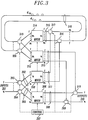
- FIG. 3 shows an illustrative packet switching system that is partitioned into multiple switches front-ended by routers.
- the modular design illustrated in FIG. 3, partitions a packet switch into a "memory block" comprised of memoryless non-blocking switching blocks (MNSB) 306, 312, 314, and 330, delay lines 318-1 to 318-m, and an input/output section comprised of input lines 301-1 to 301-n and output ports 340-1 to 340-n, respectively.
- MNSB memoryless non-blocking switching blocks
- 1 is configured as n ⁇ n, n ⁇ m, m ⁇ n, and m ⁇ m MNSBs, plus a number of routers 303, 304, 319, 320 and optional rear-end switches 309, 310, 316 and 317 for certain implementations.
- the packet switching system that is illustrated in the block diagram of FIG. 3 includes routers 303, 304, 320 and 319 that directs packets to either a delay-line MNSB, such as MNSB 314 (330) or an output MNSB such as MNSB 312 (306).
- MNSB is connected to n routers that receive incoming packets from input lines 301-1 to 303-n or m routers that receive recirculated packets from recirculation delay lines 318-1 to 318-m.
- routers 303 and 304 also perform a power splitting function that allows a control 307 to tap a small fraction of a packet's energy to read that packet's header.
- the packet switching system that is illustrated in the block diagram of FIG. 3 shares some common elements with the packet switch shown in FIG. 1.
- the packet switching system of FIG. 3 uses a) the same set of recirculation delay lines shown in FIG. 1, and b) a similar control structure, albeit with a slightly more distributed implementation.
- the control table illustrated in FIG. 2 is readily applicable to the modular design of FIG. 3.
- Control 307 is responsible for all routing decisions, including deciding which delay lines buffer which packets. For example, when multiple incoming packets destined for the same output port are received by routers 303 or 304 from input lines 301-1 to 301-n, the headers of these packets are read by control 307 which decides the proper treatment for the received packets using, for example, the scheduling techniques described above. As part of that decision, control 307 determines which packet among the received packets to send to the appropriate output port based on the priority level of the packets. The selected packet to be routed to the output port is sent to MNSB 306 which promptly forwards that packet to rear-end switch 309 or 310 via line 308.
- Rear-end switch is used in optical implementations of the packet switching system of FIG. 3 to prevent energy loss that could result from the use of other types of devices.
- control 307 sends a signal to router 303 or 304 to forward that packet to MNSB 330 which in turn sends the packet to the delay line indicated by control 307.
- buffering packets in the recirculation delay lines offers flexibility and efficiency not possible with other techniques. For example, if first-in first-out requirements dictate that an arriving packet cannot be transmitted for at least k time slots (because other packets are queued for the same output), then, it is advantageous to store that packet in a recirculation delay line of length k (if possible) and transmit that packet in due time. Even if the packet cannot be buffered in a delay line of length k, "optimal performance" may still be possible since there may be many combinations of delay-line lengths that sum to k.
- an optimal (i.e., minimal) delay of 10 time slots can be attained by buffering a packet in a delay line of length 10, or by buffering it successively in delay lines of length 7 and 3, or successive delay lines of length 6, 1, and 3, etc.
- recirculation permits "scheduling decisions" to be-revised each time a packet returns to the switch from the feedback delay lines (e.g., to allow for quicker transmission of new higher-priority packets).
Landscapes
- Engineering & Computer Science (AREA)
- Computer Networks & Wireless Communication (AREA)
- Signal Processing (AREA)
- Data Exchanges In Wide-Area Networks (AREA)
Abstract
Description
- This invention relates to switching systems. More specifically, this invention relates to the scheduling of packet delivery in a switching system.
- Because of the unscheduled nature of arrivals of packets or ATM cells to a packet switching system, two or more packets may simultaneously arrive on different inputs destined for the same output. The switch architecture may allow one of these packets to pass through to the output, but the others must be queued for later transmissions. This temporary congestion caused by simultaneous arrival of packets or cells is typically handled by temporarily storing the packets or cells in buffers. For traffic distributions that are random or more or less uniform, buffering requirements are rather lenient. However, for high performance packet switching systems designed to handle bursty traffic, the buffering requirements are more stringent.
- For electronic packet switches, buffering is ordinarily implemented in a random access memory (RAM) that is typically shared by all the inputs and outputs of the switch in order to reduce memory storage requirements. In optical packet switches, the present lack of an optical random access memory significantly complicates buffering in those optical switches. Approaches that have been considered for buffering in optical switches include an implementation that involves the routing of queued packets to trap lines that retard the transmission of the queued input packets to the desired output, thereby allowing other input packets destined for the same output to be transmitted during the delay period. However, this approach presents certain drawbacks that prevent its use in optical and optoelectronic packet switches. Specifically, certain scheduling functions needed for the orderly and timely switching and transmission of packets are not performed in the trap line approach. For example, the trap line approach (unlike the RAM approach) does not permit changes to the "scheduled" transmission time of lower-priority packets when higher-priority packets arrive later.
- Another approach that has been advocated for buffering packets in optical switches is the so-called "feed-forward" technique in which packets contending for an output port are delayed by different numbers of time slots to avoid collision with previously scheduled packets. In that approach, packets are dropped if they cannot be scheduled in a collision-free manner. This approach, however, does not allow transmission time to be updated on a slot-by-slot basis and does not adequately support priority traffic.
- Thus, there is a need for a packet buffering system for use in optical and optoelectronic packet switches which offers the same performance and functionality provided by a RAM in electronic packet switches.
- This invention is directed to a packet switch in which incoming packets or cells destined for a common output port are analyzed to determine their priority level. Lower-priority packets or cells are buffered in recirculation delay lines of appropriately-selected lengths, and thereafter are scheduled for transmission to the output ports based on their level of priority.
- In a specific example of the invention, a memoryless non-blocking switch is designed to include an input/output section comprised of a certain number of input ports and output ports and a certain number of recirculation delay lines of various lengths connected to dedicated input and output ports for buffering packets. The switch also includes control circuitry that determines which packets need to be buffered in the recirculation delay lines and schedules the delivery of the buffered packets based on their priority level. The control circuitry also keeps packets in their proper first-in, first-out sequence, supports multiple levels of priority traffic, and ensures that packets pass through the recirculation delay lines only a small number of times to minimize power losses, thereby avoiding the need for optical amplifiers in the delay lines in most cases. If amplifiers are used, a reduced number of lines through which a packet has to travel results in a proportional decrease in amplifier noise.
- In another example of the invention, a packet switching system is partitioned into multiple, memoryless, non-blocking switches that are either connected to recirculation delay lines or to the output ports of the packet switching system. The first group of switches are called a "delay-line switches" while the second are called an "output switches". Delay-line and output switches are front-ended by routers which receive commands from a control circuitry to direct packets from input ports to either a delay-line switch when the packets must be queued or to an output switch when no queuing is required.
-
- FIG. 1 illustrates a packet switch designed in accordance with the invention to schedule delivery of lower-priority packets based on their priority level and to buffer packets in recirculation delay lines of appropriately-selected lengths;
- FIG. 2 shows one example of a control table which keeps track of packets in the recirculation delay lines of FIGs. 1 and 3; and
- FIG. 3 shows an illustrative packet switching system that is partitioned into multiple switches front-ended by routers.
- FIG. 1 illustrates an example of a packet switch which schedules delivery of packets based on their priority level. The packet switch of FIG. 1 also buffers lower-priority packets in recirculation delay lines of appropriately-selected lengths. FIG. 1 shows a block diagram of a n×n packet switch comprising a) n input lines 101-1 to 101-n b) n output ports 103-1 to 103-n c) m recirculation delay lines (of appropriately-selected lengths) 105-1 to 105-m for buffering packets d) an (n+m)×(n+m) memoryless, non-blocking
switching block 102, and e) acontrol circuit 104 which reconfigures theswitching block 102 on a packet-by-packet basis. In FIG. 1, packets arrive at the input lines 101-1 to 101-n of theswitching block 102. While switchingblock 102 can be a strictly non-blocking switching block, it is preferably a rearrangeably non-blocking switching block. For optical implementations, input lines 101-1 to 101-n may be fiber lines. When there is no contention for the output ports, packets received from input lines 101-1 to 101-n are transmitted to the appropriate output ports 102-1 to 102-n based on the packet headers that indicate the destination point for each packet. The header of a packet is read bycontrol 104 which uses power splitters 110-1 to 110-n to tap a small fraction of the packet energy to read the header. To determine the appropriate configuration of theswitching block 102,control 104 keeps track of all packets buffered in the recirculation delay lines 105-1 to 105-m, so that it knows which packets will be returning to theswitching block 102 at what times.Control 104 may be implemented using, for example, a microprocessor which executes programming instructions described below. - FIG. 1 shows that the recirculation delay lines 105-1 to 105-m have lengths d₁, d₂, ..., and dm. The lengths of those lines are expressed in units equal to the number of packets that they respectively can store end-to-end. In order to explain the interaction between
switching block 102,control 104 and recirculation lines 105-1 to 105-m, it is assumed in this example, (without loss of generality, and for the sake of simplicity) that d₁ ≦ d₂ ≦ ··· ≦ dm. For illustrative purposes, special attention is devoted to the case in which d₁ = 1, d₂ = 2, ..., and dm = m. Since a total of B(d₁ + d₂ + ··· + dm) packets can be stored in the recirculation delay lines 105-1 to 105-m, it follows that B = m(m+1)/2 when d₁ = 1, d₂ = 2, ..., and dm = m. It is further assumed that switching
block 102 andcontrol circuit 104 use a time-slotted system in which, for each time slot, up to (n+m) packets may arrive at the switch (i.e., n new arrivals plus m "recirculation packets"). Of these packets, up to n can be transmitted to their appropriate output ports; the rest are "buffered" in the recirculation delay lines 105-1 to 105-m. A packet that is buffered in a recirculation delay line of length di will exit that delay line and return to switchingblock 102 after di time slots.Control 104 selects which packets to output for each time slot, and also assigns the remaining packets to the recirculation delay lines. More specifically,control 104 assigns packets to the appropriate delay lines in a way such that "buffer locations" in the delay lines are efficiently utilized, and packets retain their proper first-in, first-out sequence, as needed.Control 104 also ensures that each packet circulates through the delay lines 105-1 to 105-m only a small number of times. This last property is very important, because it may help to keep the power losses low enough to reduce, and perhaps eliminate, the need for optical amplifiers in the recirculation delay lines 105-1 to 105-m. If amplifiers are needed in the recirculation delay lines 105-1 to 105-m, minimization of the number of recirculations helps keep the added noise sufficiently small. In addition, if the power budget does indicate the need for amplifiers in the recirculation delay lines 105-1 to 105-m, the reduction in the number of lines translates into a valuable reduction in the number of amplifiers. - It may be important to note that many different technologies can potentially be used for an optical implementation of the switch illustrated in FIG. 1. For example, technologies such as guided-wave using lithium niobate; or perhaps Wavelength Diversion Multiplexing (WDM) and star couplers; or even wavelength routers can be used to build such a switch. In addition, the delay-line function that is performed in this example by the recirculation delay lines 105-1 to 105-m can be implemented using, for example, optical fiber lines or other appropriate optical transmission means. As to the
control circuitry 104, it can more easily be implemented using a microprocessor even though it is also possible to use optical logic gates to design such a circuit in an optical implementation. - FIG. 2 shows one exemplary structure of a control table which is arranged to keep track of packets in the recirculation delay lines of FIG. 1 described above and FIG. 3 described below.
- In order to free
control circuit 104 of FIG. 1 of the task of reading (for each time slot) the headers of all packets exiting the recirculation delay lines 105-1 to 105-m,control circuitry 104 maintains a table of information about the packets stored in the recirculation delay lines 105-1 to 105-m. FIG. 2 illustrates one possible way forcontrol 104 to store information about the buffered packets. As mentioned above, this information (e.g., the packets' output port addresses) is obtained by reading the packet headers when they first arrive to theswitching block 102. This information is kept in the control table of FIG. 2 until the packet exits theswitching block 102. In this example, the table of FIG. 2 is an m×dm table in an (electronic) RAM, that operates at the packet rate and that is arranged to mimic the flow of packets through the recirculation delay lines 105-1 to 105-m. Each row in the table corresponds to one of the m delay lines (m = 8 in FIG. 2). Each column contains information corresponding to the set of packets that will exit the delay lines at the same time and arrive together for routing through theswitching block 102. The time-slot pointer shown at the bottom of FIG. 2 cyclically shifts to the left one column per time slot to indicate the current set of (up to) m recirculation packets now returning to switchingblock 102. The shaded portion of the m×dm table corresponds to unused entries (for a given position of the time-slot pointer). When a packet is buffered in a recirculation delay line, information about that packet is moved in the control table of FIG. 2 to the appropriate position along the "diagonal" (P₁₄ fordelay line 1, P₂₅ fordelay line 2, P₃₆ fordelay line 3,..., or P₈₃ for delay line 8). The amount of information associated with each of these Pij entries depends on the particular implementation ofcontrol 104, as illustrated by the following two examples. - In an illustrative non-FIFO (First-In First-Out) control implementation, the
control 104 first routes as many of the packets to their outputs as possible for each time slot. In sequence, it considers the recirculation packets (beginning at the longest delay line and moving towards the shortest delay line), and then considers the new packet arrivals. If there are multiple priorities, higher-priority packets are handled first. Whenever a packet cannot be routed to its output port j (because another packet has already been selected for routing to output j), then the packet is sent to the shortest delay line that has the fewest packets destined for that output j "in that column" of the Control Table of FIG. 2. Since at most one packet per output can be transmitted for each time slot, this last factor helps "load balance" the output addresses over the table's columns. - In an illustrative FIFO-control implementation, for each time slot, the new packet arrivals and the recirculation packets are either (i) routed to the appropriate output ports for transmission, (ii) "scheduled" for transmission after one more recirculation, or (iii) left "unscheduled" and sent to a delay line for another recirculation. Each Pij entry in the control table keeps track of (i) the input-output ports of each packet in the recirculation delay lines, and (ii) whether or not the packet is scheduled for transmission the next time it reaches the
switching block 102. There also is a FIFO table associated with each input-output pair. The FIFO keeps a first-in, first-out list of all packets of this input-output pair, the exact location of these packets in the recirculation delay lines and in which (if any) future time slots they are scheduled for transmission. Finally, a "timestamp" is given to each packet when it first arrives to theswitching block 102. The timestamp corresponds to the transmission time of an ideal output-queuing switch, and represents the packet's "anticipated transmit time." - Using this information about each packet, the Control schedules packets for transmission in the current time slot or future time slots. First, it routes any "scheduled packets" on the recirculation delay lines to the appropriate output ports. Second, it checks if any of the new arrivals can be routed to their outputs (without violating the FIFO constraint). Third, it schedules packets, if possible, for transmission after their next recirculation (on the shortest possible delay line). A packet can be scheduled only if the packet before it in its input-output FIFO has already been scheduled. Priority in this scheduling is given to packets with the smallest timestamp ("anticipated transmit time"), and to recirculation packets on the longest delay lines. Once a packet is scheduled, this may also indirectly allow other packets waiting in the same input-output FIFO to be scheduled without violating the FIFO constraint. Finally, any remaining packets are left unscheduled and are recirculated to the delay lines. Starting with unscheduled packets having the smallest timestamp, packets are sent to the shortest delay line that has the fewest packets destined for that output in that column of the control table of FIG. 2.
- Other contention resolution schemes considered include routing a packet to an output port (as opposed to a recirculation delay line) based on the position of the input port from which the packet is received when that packet is contending for an output port with another packet of equal priority level. Likewise, a packet received from a recirculation delay line dedicated input port may be routed to an output port when another packet received simulatneously from a "regular" input port is contending for the same output port. In that case, in accordance with the principles of the invention, the other packet would be routed to a recirculation delay line. priority
- FIG. 3 shows an illustrative packet switching system that is partitioned into multiple switches front-ended by routers. The modular design, illustrated in FIG. 3, partitions a packet switch into a "memory block" comprised of memoryless non-blocking switching blocks (MNSB) 306, 312, 314, and 330, delay lines 318-1 to 318-m, and an input/output section comprised of input lines 301-1 to 301-n and output ports 340-1 to 340-n, respectively. In FIG. 3, the (n+m)×(n+m) switch of FIG. 1 is configured as n×n, n×m, m×n, and m×m MNSBs, plus a number of
routers end switches - The packet switching system that is illustrated in the block diagram of FIG. 3 includes
routers routers control 307 to tap a small fraction of a packet's energy to read that packet's header. The packet switching system that is illustrated in the block diagram of FIG. 3 shares some common elements with the packet switch shown in FIG. 1. For example, the packet switching system of FIG. 3 uses a) the same set of recirculation delay lines shown in FIG. 1, and b) a similar control structure, albeit with a slightly more distributed implementation. Thus, the control table illustrated in FIG. 2 is readily applicable to the modular design of FIG. 3. - As is the case for the switch of FIG. 1, the
Control 307 is responsible for all routing decisions, including deciding which delay lines buffer which packets. For example, when multiple incoming packets destined for the same output port are received byrouters control 307 which decides the proper treatment for the received packets using, for example, the scheduling techniques described above. As part of that decision,control 307 determines which packet among the received packets to send to the appropriate output port based on the priority level of the packets. The selected packet to be routed to the output port is sent toMNSB 306 which promptly forwards that packet to rear-end switch line 308. Rear-end switch is used in optical implementations of the packet switching system of FIG. 3 to prevent energy loss that could result from the use of other types of devices. When a packet has to be buffered,control 307 sends a signal torouter control 307. - Advantageously, buffering packets in the recirculation delay lines (105-1 to 105-m in FIG. 1 or 318-1 to 318-m in FIG. 3) offers flexibility and efficiency not possible with other techniques. For example, if first-in first-out requirements dictate that an arriving packet cannot be transmitted for at least k time slots (because other packets are queued for the same output), then, it is advantageous to store that packet in a recirculation delay line of length k (if possible) and transmit that packet in due time. Even if the packet cannot be buffered in a delay line of length k, "optimal performance" may still be possible since there may be many combinations of delay-line lengths that sum to k. For example, an optimal (i.e., minimal) delay of 10 time slots can be attained by buffering a packet in a delay line of
length 10, or by buffering it successively in delay lines oflength 7 and 3, or successive delay lines oflength
Claims (18)
- A packet switching system comprising:
at least one switching block having a plurality of input and output ports;
a control circuit for determining a) priority levels of packets received by the input ports and b) delivery time of packets to the output ports;
at least one recirculation delay element; and
means for buffering packets in the at least one recirculation delay element in accordance with the priority levels determined by the control circuit. - The invention of claim 1 wherein said buffering means comprise
means for routing at least one lower-priority packet to the at least one recirculation delay element until the lower-priority packet is no longer in contention for the output port with at least one higher-priority packet; and
means for keeping track of all packets routed to all recirculation delay elements. - The invention of claim 2 further comprising
means for limiting the number of times a lower-priority packet is routed to a recirculation delay element. - The invention of claim 1 further comprising
means for routing a lower-priority packet to the output port after at least one higher-priority packet has been routed to said output port. - The invention of claim 1 wherein the packet switching system has more than one recirculation delay elements of different time-delaying means and wherein a packet is buffered in a particular recirculation delay element based on its priority level.
- The invention of claim 5 wherein lower-priority packets are buffered in longer-time-delaying-means element and higher-priority packets are buffered in shorter-time-delaying-means element.
- The invention of claim 1 wherein each recirculation delay element is a fiber-optic line that is of a particular length and that is connected to a dedicated input and output port of a switching block.
- The invention of claim 1 further comprising
means for keeping all packets routed to an output port of the switching block in a first-in first-out sequence. - Apparatus for use in a packet switching system comprising:
means for determining the level of priority of incoming packets received from different input ports of the packet switching system and destined for a common output port of the packet switching system;
routing a higher-priority packet to the output port;
means for buffering in at least one recirculation delay line at least one lower-priority packet; and
means for scheduling delivery to the output port of the at least one lower-priority packet buffered in the recirculation delay lines. - The apparatus of claim 9 wherein the scheduling means comprises:
means for routing at least once the at least one lower-priority packet to the recirculation delay lines. - The invention of claim 10 further comprising
means for limiting the number of times a lower-priority packet can be routed to the at least one recirculation delay line. - A method of routing packets in a switch comprising
determining levels of priority of incoming packets received from different input ports of the switch and destined for a common output port of the switch;
routing a higher-priority packet to the output port;
buffering in at least one recirculation delay line at least one lower-priority packet; and
scheduling delivery to the output port of the at least one lower-priority packet buffered in the at least one recirculation delay line. - A packet switching system comprising:
a switching fabric having at least one switching block with a plurality of input and output ports;
a control circuit for determining levels of priority for packets received from the input ports;
at least one recirculation delay element which is connected to a dedicated input port and a dedicated output port of the switching fabric and through which, a particular packet exiting the switching fabric is returned to the switching fabric at least once; and
means for queuing at least one packet in the at least one recirculation delay element in response to a signal from the control circuit. - The invention of claim 13 wherein the signal is emitted by the control circuit if at least two packets are received simultaneously on different input ports and are destined for a common output port.
- The invention of claim 13 wherein the signal from the control circuit is a function of the priority levels of the received packets and programming instructions in said circuit.
- The invention of claim 15 further comprising
means for routing at least one lower-priority packet to the at least one recirculation delay element at least once. - The invention of claim 15 further comprising
means for routing a queued packet to an output port when the queued packet is in contention for the output port with another packet of equal priority level. - The invention of claim 15 further comprising
means for routing a packet to an output port based on the position of the input port from which said packet is received when said packet is in contention with another packet of equal priority level.
Applications Claiming Priority (2)
| Application Number | Priority Date | Filing Date | Title |
|---|---|---|---|
| US08/090,732 US5416769A (en) | 1993-07-13 | 1993-07-13 | Controlled-feedback packet switching system |
| US90732 | 1993-07-13 |
Publications (3)
| Publication Number | Publication Date |
|---|---|
| EP0634854A2 true EP0634854A2 (en) | 1995-01-18 |
| EP0634854A3 EP0634854A3 (en) | 1996-01-10 |
| EP0634854B1 EP0634854B1 (en) | 2002-10-09 |
Family
ID=22224054
Family Applications (1)
| Application Number | Title | Priority Date | Filing Date |
|---|---|---|---|
| EP94304973A Expired - Lifetime EP0634854B1 (en) | 1993-07-13 | 1994-07-06 | Controlled-feedback packet switching system |
Country Status (5)
| Country | Link |
|---|---|
| US (1) | US5416769A (en) |
| EP (1) | EP0634854B1 (en) |
| JP (1) | JP3190522B2 (en) |
| CA (1) | CA2124471C (en) |
| DE (1) | DE69431502T2 (en) |
Cited By (3)
| Publication number | Priority date | Publication date | Assignee | Title |
|---|---|---|---|---|
| EP0808045A3 (en) * | 1996-05-09 | 2000-05-10 | Nippon Telegraph And Telephone Corporation | ATM switch |
| SG97939A1 (en) * | 1999-09-30 | 2003-08-20 | Cit Alcatel | Control architecture in optical burst-switched networks |
| US6947446B2 (en) | 2001-01-16 | 2005-09-20 | Motorola, Inc. | Slot format and acknowledgement method for a wireless communication system |
Families Citing this family (56)
| Publication number | Priority date | Publication date | Assignee | Title |
|---|---|---|---|---|
| US5617413A (en) * | 1993-08-18 | 1997-04-01 | The United States Of America As Represented By The Administrator Of The National Aeronautics And Space Administration | Scalable wrap-around shuffle exchange network with deflection routing |
| JP3044983B2 (en) | 1993-08-25 | 2000-05-22 | 株式会社日立製作所 | Cell switching method for ATM switching system |
| JP2596718B2 (en) * | 1993-12-21 | 1997-04-02 | インターナショナル・ビジネス・マシーンズ・コーポレイション | How to manage network communication buffers |
| FR2715015B1 (en) * | 1994-01-07 | 1996-02-02 | Auffret Rene | Method and device for transmitting and routing packets in an optical network. |
| IT1266895B1 (en) * | 1994-07-26 | 1997-01-21 | Cselt Centro Studi Lab Telecom | PROCEDURE FOR THE OPTIMUM ALLOCATION OF RESOURCES FOR THE TRANSPORT OF VARIABLE BAND INFORMATION FLOWS ON NETWORKS IN ATM TECHNIQUE, AND NODE |
| US5923657A (en) * | 1994-08-23 | 1999-07-13 | Hitachi, Ltd. | ATM switching system and cell control method |
| US5500858A (en) * | 1994-12-20 | 1996-03-19 | The Regents Of The University Of California | Method and apparatus for scheduling cells in an input-queued switch |
| US5636210A (en) * | 1995-08-02 | 1997-06-03 | Agrawal; Jagannath P. | Asynchronous transfer mode packet switch |
| FR2742894B1 (en) * | 1995-12-20 | 1998-03-13 | Deroux Dauphin Patrice | SYSTEM FOR EXCHANGING INFORMATION BETWEEN SEVERAL OPERATORS |
| EP0790750B1 (en) * | 1996-02-16 | 2005-05-25 | Alcatel | Optical switch with synchronisation |
| US5822300A (en) * | 1996-04-02 | 1998-10-13 | Compaq Computer Corporation | Congestion management scheme |
| US5889776A (en) * | 1997-01-31 | 1999-03-30 | Alpnet Corporation | Physical layer switch system for ethernet local area network communication system |
| US6362905B1 (en) * | 1997-02-24 | 2002-03-26 | Hitachi, Ltd. | Optical crossconnect apparatus and optical transmission system |
| US5991302A (en) * | 1997-04-10 | 1999-11-23 | Cisco Technology, Inc. | Technique for maintaining prioritization of data transferred among heterogeneous nodes of a computer network |
| US6791979B1 (en) | 1997-04-10 | 2004-09-14 | Cisco Technology, Inc. | Mechanism for conveying data prioritization information among heterogeneous nodes of a computer network |
| US5940390A (en) * | 1997-04-10 | 1999-08-17 | Cisco Technology, Inc. | Mechanism for conveying data prioritization information among heterogeneous nodes of a computer network |
| US6115751A (en) * | 1997-04-10 | 2000-09-05 | Cisco Technology, Inc. | Technique for capturing information needed to implement transmission priority routing among heterogeneous nodes of a computer network |
| US5987028A (en) * | 1997-05-12 | 1999-11-16 | Industrial Technology Research Insitute | Multiple channel ATM switch |
| KR100233103B1 (en) | 1997-05-27 | 1999-12-01 | 윤종용 | Apparatus and method for optical switch having circulating structure |
| US6289389B1 (en) * | 1997-06-03 | 2001-09-11 | Lextron Systems, Inc. | Enhanced integrated data delivery system |
| US6088734A (en) * | 1997-11-12 | 2000-07-11 | International Business Machines Corporation | Systems methods and computer program products for controlling earliest deadline first scheduling at ATM nodes |
| US6065062A (en) * | 1997-12-10 | 2000-05-16 | Cisco Systems, Inc. | Backup peer pool for a routed computer network |
| US6185021B1 (en) * | 1998-03-20 | 2001-02-06 | Lucent Technologies, Inc. | Cross-connecting optical translator array |
| US6154743A (en) * | 1998-06-16 | 2000-11-28 | Cisco Technology, Inc. | Technique for accessing heterogeneous directory services in an APPN environment |
| US6145032A (en) * | 1998-09-21 | 2000-11-07 | International Business Machines Corporation | System for recirculation of communication transactions in data processing in the event of communication stall |
| US6947415B1 (en) * | 1999-04-15 | 2005-09-20 | Nortel Networks Limited | Method and apparatus for processing packets in a routing switch |
| JP3339463B2 (en) * | 1999-05-13 | 2002-10-28 | 日本電気株式会社 | Switch and its input port |
| US6810211B1 (en) * | 1999-09-08 | 2004-10-26 | Alcatel | Preferred WDM packet-switched router architecture and method for generating same |
| US6819870B1 (en) | 1999-11-02 | 2004-11-16 | Alcatel | All-optical networking optical fiber line delay buffering apparatus and method |
| US6671256B1 (en) | 2000-02-03 | 2003-12-30 | Alcatel | Data channel reservation in optical burst-switched networks |
| US6570694B1 (en) | 2000-03-03 | 2003-05-27 | Alcatel | System and method for low-jitter asynchronous optical regeneration using wavelength sampling |
| US6763192B1 (en) | 2000-03-03 | 2004-07-13 | Alcatel | Integration of all-optical crossconnect functionality in an optical packet switching apparatus |
| US6728212B1 (en) | 2000-06-23 | 2004-04-27 | Alcatel | Asymmetric void filling scheduler with bandwidth grabbing |
| US6804255B1 (en) | 2000-10-12 | 2004-10-12 | Alcatel | Hardware implementation of channel scheduling algorithms for optical routers with FDL buffers |
| US7221677B1 (en) * | 2000-10-19 | 2007-05-22 | Interactic Holdings, Llc | Scalable apparatus and method for increasing throughput in multiple level minimum logic networks using a plurality of control lines |
| US6665495B1 (en) * | 2000-10-27 | 2003-12-16 | Yotta Networks, Inc. | Non-blocking, scalable optical router architecture and method for routing optical traffic |
| US6963564B1 (en) * | 2000-12-22 | 2005-11-08 | Alcatel | Method and apparatus for synchronized slotted optical burst switching |
| US20020154360A1 (en) * | 2000-12-22 | 2002-10-24 | Liu Heyun H. | Discrete time sequence model for slotted and synchronous switching of optical burst signals |
| FR2819665B1 (en) * | 2001-01-15 | 2003-04-11 | Cit Alcatel | PHOTON SWITCHING DEVICE |
| US7426210B1 (en) | 2001-04-03 | 2008-09-16 | Yt Networks Capital, Llc | Port-to-port, non-blocking, scalable optical router architecture and method for routing optical traffic |
| US7068603B2 (en) * | 2001-07-06 | 2006-06-27 | Juniper Networks, Inc. | Cross-bar switch |
| US7190900B1 (en) * | 2001-07-20 | 2007-03-13 | Lighthouse Capital Partners Iv, Lp | System and method for implementing dynamic scheduling of data in a non-blocking all-optical switching network |
| US7106697B1 (en) * | 2001-07-20 | 2006-09-12 | Lighthouse Capital Partners, Iv, Lp | Method for dynamically computing a switching schedule |
| US7218637B1 (en) | 2001-07-20 | 2007-05-15 | Yotta Networks, Llc | System for switching data using dynamic scheduling |
| KR100419609B1 (en) * | 2001-10-29 | 2004-02-25 | 주식회사 케이티 | Apparatus for scheduling cell/packet in switching system |
| US7613200B1 (en) * | 2002-01-15 | 2009-11-03 | Cisco Technology, Inc. | Method and apparatus using a random indication to map items to paths and to recirculate or delay the sending of a particular item when a destination over its mapped path is unreachable |
| TWI239156B (en) * | 2003-09-18 | 2005-09-01 | Ind Tech Res Inst | Multi-wavelength optical packet switch system with shared output buffer |
| US8107822B2 (en) * | 2005-05-20 | 2012-01-31 | Finisar Corporation | Protocols for out-of-band communication |
| US20070260728A1 (en) * | 2006-05-08 | 2007-11-08 | Finisar Corporation | Systems and methods for generating network diagnostic statistics |
| US7899057B2 (en) * | 2006-04-28 | 2011-03-01 | Jds Uniphase Corporation | Systems for ordering network packets |
| US8213333B2 (en) * | 2006-07-12 | 2012-07-03 | Chip Greel | Identifying and resolving problems in wireless device configurations |
| CN101212818B (en) * | 2006-12-26 | 2010-12-08 | 华为技术有限公司 | Network node, cache device and scheduling method |
| US8526821B2 (en) | 2006-12-29 | 2013-09-03 | Finisar Corporation | Transceivers for testing networks and adapting to device changes |
| US8260142B2 (en) * | 2009-06-29 | 2012-09-04 | Alcatel Lucent | Multi-channel optical arrayed time buffer |
| JP5987915B2 (en) * | 2012-11-12 | 2016-09-07 | 日本電気株式会社 | Communication relay device, communication relay system, communication relay method, and communication relay program |
| JP6341601B2 (en) * | 2014-04-01 | 2018-06-13 | 国立研究開発法人情報通信研究機構 | Wavelength demultiplexer and wavelength multiplexer using the same |
Family Cites Families (8)
| Publication number | Priority date | Publication date | Assignee | Title |
|---|---|---|---|---|
| US4472801A (en) * | 1983-03-28 | 1984-09-18 | At&T Bell Laboratories | Distributed prioritized concentrator |
| US4761780A (en) * | 1986-12-22 | 1988-08-02 | Bell Communications Research, Inc. | Enhanced efficiency Batcher-Banyan packet switch |
| GB8720605D0 (en) * | 1987-09-02 | 1987-10-07 | British Telecomm | Communications switch |
| US4893304A (en) * | 1988-09-02 | 1990-01-09 | Bell Communications Research, Inc. | Broadband packet switch with combined queuing |
| US4866701A (en) * | 1988-09-02 | 1989-09-12 | Bell Communications Research, Inc. | Packet switch with dynamic allocation of inputs |
| US4891803A (en) * | 1988-11-07 | 1990-01-02 | American Telephone And Telegraph Company | Packet switching network |
| CA1320257C (en) * | 1989-04-20 | 1993-07-13 | Ernst August Munter | Method and apparatus for input-buffered asynchronous transfer mode switching |
| US5233606A (en) * | 1991-08-02 | 1993-08-03 | At&T Bell Laboratories | Arrangement for controlling shared-buffer-memory overflow in a multi-priority environment |
-
1993
- 1993-07-13 US US08/090,732 patent/US5416769A/en not_active Expired - Lifetime
-
1994
- 1994-05-27 CA CA002124471A patent/CA2124471C/en not_active Expired - Fee Related
- 1994-07-06 DE DE69431502T patent/DE69431502T2/en not_active Expired - Fee Related
- 1994-07-06 EP EP94304973A patent/EP0634854B1/en not_active Expired - Lifetime
- 1994-07-11 JP JP18041494A patent/JP3190522B2/en not_active Expired - Fee Related
Cited By (4)
| Publication number | Priority date | Publication date | Assignee | Title |
|---|---|---|---|---|
| EP0808045A3 (en) * | 1996-05-09 | 2000-05-10 | Nippon Telegraph And Telephone Corporation | ATM switch |
| SG97939A1 (en) * | 1999-09-30 | 2003-08-20 | Cit Alcatel | Control architecture in optical burst-switched networks |
| US6947446B2 (en) | 2001-01-16 | 2005-09-20 | Motorola, Inc. | Slot format and acknowledgement method for a wireless communication system |
| DE10295696B4 (en) * | 2001-01-16 | 2007-11-29 | Motorola, Inc., Schaumburg | Slot format and acknowledgment method for a wireless communication system |
Also Published As
| Publication number | Publication date |
|---|---|
| CA2124471C (en) | 1998-09-01 |
| DE69431502D1 (en) | 2002-11-14 |
| JPH07154423A (en) | 1995-06-16 |
| CA2124471A1 (en) | 1995-01-14 |
| EP0634854A3 (en) | 1996-01-10 |
| JP3190522B2 (en) | 2001-07-23 |
| DE69431502T2 (en) | 2003-06-18 |
| EP0634854B1 (en) | 2002-10-09 |
| US5416769A (en) | 1995-05-16 |
Similar Documents
| Publication | Publication Date | Title |
|---|---|---|
| US5416769A (en) | Controlled-feedback packet switching system | |
| Karol | Shared-memory optical packet (ATM) switch | |
| US5440553A (en) | Output buffered packet switch with a flexible buffer management scheme | |
| US4893304A (en) | Broadband packet switch with combined queuing | |
| Iyer et al. | Analysis of a packet switch with memories running slower than the line-rate | |
| EP0547836B1 (en) | Optical packet switch | |
| EP0569172B1 (en) | Improved controller for input-queued packet switch | |
| CA1306790C (en) | Packet switch with dynamic allocation of inputs | |
| US7756013B2 (en) | Packet switching system and method | |
| US6944170B2 (en) | Switching arrangement and method | |
| US6487171B1 (en) | Crossbar switching matrix with broadcast buffering | |
| JPH10285186A (en) | ATM switch queuing system | |
| US6574232B1 (en) | Crossbar switch utilizing broadcast buffer and associated broadcast buffer management unit | |
| EP1215931A1 (en) | Distributed scheduler for packet switches and passive optical networks | |
| Turner | WDM burst switching for petabit data networks | |
| Hsu et al. | On the deflection routing in QoS supported optical burst-switched networks | |
| US20060104281A1 (en) | Packet routing | |
| US7269158B2 (en) | Method of operating a crossbar switch | |
| Chevalier et al. | A new packet routing strategy for ultra-fast photonic networks | |
| Wang et al. | Efficient designs of optical LIFO buffer with switches and fiber delay lines | |
| KR0183341B1 (en) | AMT-PBX's Multi-Input Buffer Type ATM Switch | |
| US20020093704A1 (en) | Photonic switching device | |
| EP1198098B1 (en) | Switching arrangement and method with separated output buffers | |
| KR100382144B1 (en) | Latency compensation method for input and output buffered switch | |
| Anan et al. | A real-time hardware-based scheduler for next-generation optical burst switches |
Legal Events
| Date | Code | Title | Description |
|---|---|---|---|
| PUAI | Public reference made under article 153(3) epc to a published international application that has entered the european phase |
Free format text: ORIGINAL CODE: 0009012 |
|
| AK | Designated contracting states |
Kind code of ref document: A2 Designated state(s): DE FR GB |
|
| PUAL | Search report despatched |
Free format text: ORIGINAL CODE: 0009013 |
|
| AK | Designated contracting states |
Kind code of ref document: A3 Designated state(s): DE FR GB |
|
| 17P | Request for examination filed |
Effective date: 19960701 |
|
| 17Q | First examination report despatched |
Effective date: 20000121 |
|
| GRAG | Despatch of communication of intention to grant |
Free format text: ORIGINAL CODE: EPIDOS AGRA |
|
| GRAG | Despatch of communication of intention to grant |
Free format text: ORIGINAL CODE: EPIDOS AGRA |
|
| GRAH | Despatch of communication of intention to grant a patent |
Free format text: ORIGINAL CODE: EPIDOS IGRA |
|
| GRAH | Despatch of communication of intention to grant a patent |
Free format text: ORIGINAL CODE: EPIDOS IGRA |
|
| GRAA | (expected) grant |
Free format text: ORIGINAL CODE: 0009210 |
|
| AK | Designated contracting states |
Kind code of ref document: B1 Designated state(s): DE FR GB |
|
| REG | Reference to a national code |
Ref country code: GB Ref legal event code: FG4D |
|
| REF | Corresponds to: |
Ref document number: 69431502 Country of ref document: DE Date of ref document: 20021114 |
|
| ET | Fr: translation filed | ||
| PLBE | No opposition filed within time limit |
Free format text: ORIGINAL CODE: 0009261 |
|
| STAA | Information on the status of an ep patent application or granted ep patent |
Free format text: STATUS: NO OPPOSITION FILED WITHIN TIME LIMIT |
|
| 26N | No opposition filed |
Effective date: 20030710 |
|
| PGFP | Annual fee paid to national office [announced via postgrant information from national office to epo] |
Ref country code: DE Payment date: 20080722 Year of fee payment: 15 |
|
| PGFP | Annual fee paid to national office [announced via postgrant information from national office to epo] |
Ref country code: FR Payment date: 20080715 Year of fee payment: 15 |
|
| PGFP | Annual fee paid to national office [announced via postgrant information from national office to epo] |
Ref country code: GB Payment date: 20080722 Year of fee payment: 15 |
|
| GBPC | Gb: european patent ceased through non-payment of renewal fee |
Effective date: 20090706 |
|
| REG | Reference to a national code |
Ref country code: FR Ref legal event code: ST Effective date: 20100331 |
|
| PG25 | Lapsed in a contracting state [announced via postgrant information from national office to epo] |
Ref country code: FR Free format text: LAPSE BECAUSE OF NON-PAYMENT OF DUE FEES Effective date: 20090731 |
|
| PG25 | Lapsed in a contracting state [announced via postgrant information from national office to epo] |
Ref country code: GB Free format text: LAPSE BECAUSE OF NON-PAYMENT OF DUE FEES Effective date: 20090706 |
|
| PG25 | Lapsed in a contracting state [announced via postgrant information from national office to epo] |
Ref country code: DE Free format text: LAPSE BECAUSE OF NON-PAYMENT OF DUE FEES Effective date: 20100202 |