EP0634836A2 - Distributed amplifier and bidirectional amplifier - Google Patents
Distributed amplifier and bidirectional amplifier Download PDFInfo
- Publication number
- EP0634836A2 EP0634836A2 EP94109213A EP94109213A EP0634836A2 EP 0634836 A2 EP0634836 A2 EP 0634836A2 EP 94109213 A EP94109213 A EP 94109213A EP 94109213 A EP94109213 A EP 94109213A EP 0634836 A2 EP0634836 A2 EP 0634836A2
- Authority
- EP
- European Patent Office
- Prior art keywords
- distributed
- amplifier
- terminal
- side circuit
- input
- Prior art date
- Legal status (The legal status is an assumption and is not a legal conclusion. Google has not performed a legal analysis and makes no representation as to the accuracy of the status listed.)
- Withdrawn
Links
Images


Classifications
-
- H—ELECTRICITY
- H03—ELECTRONIC CIRCUITRY
- H03F—AMPLIFIERS
- H03F3/00—Amplifiers with only discharge tubes or only semiconductor devices as amplifying elements
- H03F3/60—Amplifiers in which coupling networks have distributed constants, e.g. with waveguide resonators
- H03F3/605—Distributed amplifiers
- H03F3/607—Distributed amplifiers using FET's
Definitions
- the present invention relates to a distributed amplifier and a bidirectional amplifier including the distributed amplifier.
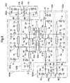
- FIG. 7 is a circuit diagram illustrating a structure of a prior art distributed amplifier.
- a distributed amplifier 700 comprises an input side circuit 70a disposed between an input terminal and ground, an output side circuit 70b disposed between an output terminal 2 and ground, and source-grounded FETs 70c and 70d disposed between the input circuit 70a and the output circuit 70b.
- the input side circuit 70a comprises three distributed constant lines 3a to 3c, a terminal resistor 8 of 50 ⁇ , and a bypass capacitor 9 which are connected in series between the input terminal 1 and ground.
- the output side circuit 70b comprises three distributed constant lines 3d to 3f, a terminal resistor 8 of 50 ⁇ , and a bypass capacitor 9 which are connected in series between the output terminal 2 and ground.
- the source-grounded FET 70c includes a gate connected to the junction of the input side distributed constant lines 3a and 3b and a drain connected to the junction of the output side distributed constant lines 3e and 3f via a distributed constant line 10.
- the source-grounded FET 70c includes a gate connected to the junction of the input side distributed constant lines 3b and 3c and a drain connected to the junction of the output side distributed constant lines 3d and 3e via a distributed constant line 10.
- Each of the source-grounded FETs 70c and 70d is illustrated as an equivalent circuit comprising a gate-to-source capacitance 4, a current supply 5 controlled by a gate bias voltage, and a drain-to-source capacitance 6.
- the distributed constant lines 3a to 3c of the input side circuit 70a on the gate side of the source-grounded FET 70c (70d) is regarded as an inductance (Lg)
- the gate-source capacitance (Cgs) 4 of the FET and the inductance (Lg) form a circuit equivalent to a distributed constant line on the gate side of the FET.
- the distributed constant line 10 connected to the drain of the source-grounded FET 70c (70d) is regarded as an inductance (Ld)
- the drain-source capacitance (Cds) 6 of the FET and the inductance (Ld) form a circuit equivalent to a distributed constant line on the drain side of the FET.
- the following equation (3) is achieved on the gate side of the source-grounded FET 70c (70d).
- the cut-off frequency fc is represented by The same relationship as described above is achieved on the drain side of the FET. Further, the input signal is amplified by the FET.
- this distributed amplifier 700 is a broadband amplifier that can be used until the cut-off frequency.
- T/R Transmit/Receive
- two distributed amplifiers 700 serving as a transmitter and a receiver, respectively, are required and, in addition, a T/R switch of a frequency band as wide as or wider than that of the distributed amplifier is required for switching the signal input-output path between the transmitter and the receiver. Therefore, if a T/R module is fabricated using the prior art distributed amplifiers 700, the chip size of the T/R module is unfavorably increased by the T/R switch. Further, the signal transmission loss due to the T/R switch must be considered.
- a distributed amplifier comprises an input side circuit including a plurality of distributed constant lines connected in series between an input terminal and ground, and a plurality of source-grounded FETs for switching operation having drains connected to junctions between the distributed constant lines of the input side circuit; an output side circuit including a plurality of distributed constant lines connected in series between an output terminal and ground; and a plurality of source-grounded amplifier FETs each having a gate connected to the junction of the distributed constant lines of the input side circuit via a capacitor and a drain connected to the junction of the distributed constant lines of the output side circuit.
- the input side circuit also serves as a distributed switch, when a T/R module is fabricated using the distributed amplifier, no additional distributed switch for controlling signal input and output is needed, so that the chip size of the T/R module is reduced compared to the conventional T/R module. In addition, signal transmission loss is reduced.
- a bidirectional amplifier comprises first and second distributed amplifiers of the same structure as described above, and first and second SPDT (single Pole Double Throw) switches each having first, second, and third terminals wherein an input signal applied to the first terminal is output from one of the second and third terminals, or one of two input signals respectively applied to the second and third terminals is output from the first terminal.
- first and second SPDT single Pole Double Throw
- One of the second and third terminals of the first SPDT switch is connected to an input terminal of the first distributed amplifier and the other is connected to an output terminal of the second distributed amplifier.
- One of the second and third terminals of the second SPDT switch is connected to an output terminal of the first distributed amplifier and the other is connected to an input terminal of the second distributed amplifier.
- the first terminals of the first and second SPDT switches are input-output terminals of the whole circuit.
- the bidirectional amplifier is fabricated using only two distributed amplifiers and two SPDT switches with no additional distributed switch, the chip size of the amplifier is reduced compared to the conventional bidirectional amplifier, and the signal transmission loss is reduced.
- a bidirectional amplifier comprises first and second SPDT switches of the same structure as described above and a distributed amplifier.
- the distributed amplifier comprises a plurality of dual gate FETs for amplification each having first and second gates, a source, and a drain, first and second input side circuits of the same structure as described above respectively connected to the first gates and the second gates of the dual gate FETs, and first and second output side circuits of the same structure as described above respectively connected to the sources and the drains of the dual gate FETs.
- the second terminal of the first SPDT switch is connected to an input terminal of the first input side circuit, and the third terminal is connected to an output terminal of the first output side circuit.
- the second terminal of the second SPDT switch is connected to an input terminal of the second input side circuit, and the third terminal is connected to an output terminal of the second output side circuit.
- the first terminals of the first and second SPDT switches are input-output terminals of the whole circuit.
- Figure 1 is a circuit diagram illustrating a distributed amplifier in accordance with a first embodiment of the present invention.
- Figure 2 is a circuit diagram illustrating a distributed amplifier in accordance with a second embodiment of the present invention.
- Figure 3 is a circuit diagram illustrating a distributed amplifier in accordance with a third embodiment of the present invention.
- Figure 4 is a circuit diagram illustrating a distributed amplifier in accordance with a fourth embodiment of the present invention.
- Figure 5 is a circuit diagram illustrating a bidirectional amplifier in accordance with a fifth embodiment of the present invention.
- Figure 6 is a circuit diagram illustrating a bidirectional amplifier in accordance with a sixth embodiment of the present invention.
- Figure 7 is a circuit diagram illustrating a distributed amplifier in accordance with the prior art.
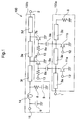
- FIG 1 is a circuit diagram illustrating a distributed amplifier in accordance with a first embodiment of the present invention.
- a distributed amplifier 100 comprises an input side circuit 100a disposed between an input terminal 1 and ground, an output side circuit 100b disposed between an output terminal 2 and ground, and source-grounded FETs 7a and 7b disposed between the input side circuit 100a and the output side circuit 100b.
- the source-grounded FETs 7a and 7b are amplifier FETs.
- the FET 7a includes a gate connected through a capacitor 9a to the junction of the distributed constant lines 3a and 3b of the input side circuit 100a and a drain connected to the junction of the distributed constant lines 3e and 3f of the output side circuit 100b.
- a gate bias terminal 13 is connected through a resistor 8a to the junction of the gate of the FET 7a and the capacitor 9a.
- the FET 7b includes a gate connected through a capacitor 9a to the junction of the distributed constant lines 3b and 3c of the input side circuit 100a and a drain connected to the junction of the distributed constant lines 3d and 3e of the output side circuit 100b.
- a gate bias terminal 13 is connected through a resistor 8a to the junction of the gate of the FET 7b and the capacitor 9a.
- the input side circuit 100a includes three distributed constant lines 3a to 3c and a terminal resistor 8 which are connected in series between the input terminal 1 and ground, and two source-grounded FETs 11a and 11b.
- a drain of the source-grounded FET 11a is connected to the junction of the distributed constant lines 3a and 3b, and a drain of the source-grounded FET 11b is connected to the junction of the distributed constant lines 3b and 3c.
- the distributed constant lines 3a to 3c and the FETs 11a and 11b form a distributed switch.
- a gate bias terminal 12 is connected to a gate of each FET.
- the output side circuit 100b includes three distributed constant lines 3d to 3f, a terminal resistor 8, and a bypass capacitor 9 which are connected in series between an output terminal 2 and ground.
- a drain bias terminal 15 for the source-grounded FETs 7a and 7b is connected through an RF choke coil 14 to the junction of the terminal resistor 8 and the distributed constant line 3f, and a bypass capacitor 9 is inserted between ground and the junction of the drain bias terminal 15 and the RF choke coil 14.
- the source and the drain of the source-grounded FET 11a (11b) are set at the same voltage by the terminal resistor 8, a switching operation is possible according to a bias voltage applied to the gate bias terminal 12.
- the distributed switch is turned on, and a signal is input to the input side circuit 100a and the distributed amplifier 100 operates similarly as the prior art distributed amplifier 700.
- the distributed switch is turned off, and no signal is input to the input side circuit 100a.
- the source-grounded FET 11a (11b) in the ON state has no resistance and the FET in the OFF state becomes a capacitance (CT).
- the capacitance (C) of the capacitor 9 connected to the drain of the FET 11a (11b) has the relation of C >> CT,Cgs.
- the parameters C, CT, and Cgs have to be designed so that the input side impedance Zo represented by the following equation (5) becomes 50 ⁇ , whereby the distributed amplifier 100 operates in the same manner as the prior art amplifier 700.
- the input side impedance Z must satisfy the following equation (6) so that no signal is input to the input side circuit 100a.
- the input side circuit 100a serves both as an amplifier and a switch for determining whether a signal is input to the distributed amplifier 100 or not. Therefore, when a T/R module is fabricated using this distributed amplifier 100, no additional distributed switch is needed, so that the chip size of the T/R module is reduced compared to the prior art. Further, it is not necessary to consider the signal transmission loss due to the distributed switch, so that the design of the T/R module is simplified.
- FIG 2 is a circuit diagram illustrating a distributed amplifier in accordance with a second embodiment of the present invention.
- the same reference numerals as in figure 1 designate the same or corresponding parts.
- the structure of the distributed amplifier 200 of this second embodiment is fundamentally identical to that of the first embodiment except that an inductor 16 is interposed between the source and the drain of each of the source-grounded FETs 11a and 11b included in the input side circuit.
- the working frequency (fo) is represented by and if the inductance L of the inductor 16 is designed so that the working frequency fo is a desired value, this distributed amplifier 200 is available in a narrow band.
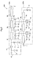
- FIG 3 is a circuit diagram illustrating a distributed amplifier in accordance with a third embodiment of the present invention.
- a distributed amplifier 300 of this third embodiment employs dual gate FETs 30a and 30b for amplification in place of the FETs 7a and 7b of the distributed amplifier 100 of the first embodiment, and a gate bias terminal 31 for controlling gain is connected to one of two gates of each dual gate FET.
- a high-performance distributed amplifier is achieved.
- FIG 4 is a circuit diagram illustrating a distributed amplifier in accordance with a fourth embodiment of the present invention.
- the same reference numerals as those in figures 2 and 3 designate the same or corresponding parts.
- a distributed amplifier 400 according to this fourth embodiment is fundamentally identical to the distributed amplifier 300 of the third embodiment except that the input side circuit 200a of the second embodiment shown in figure 2 is employed in place of the input side circuit 100a.
- the distributed amplifier 400 of this fourth embodiment provides the same effects as described in the third embodiment.
- the amplifier 400 can be used in a narrower band than the distributed amplifier 300 of the third embodiment.
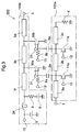
- FIG. 5 is a circuit diagram illustrating a bidirectional amplifier in accordance with a fifth embodiment of the present invention.
- a bidirectional amplifier 500 comprises two distributed amplifiers 100A and 100B of the same structure as the distributed amplifier 100 according to the first embodiment, and two SPDT (Single Pole Double Throw) switches 500a and 500b each comprising two FETs 17a and 17b.
- An input terminal 1a of the distributed amplifier 100A is connected to a first terminal 19a of the SPDT switch 500a via a capacitor 9b
- an output terminal 2b of the distributed amplifier 100B is connected to a second terminal 19b of the SPDT switch 500a via a capacitor 9b.
- An output terminal 2a of the distributed amplifier 100A is connected to a first terminal 19a of the SPDT switch 500b via a capacitor 9b, and an input terminal 1b of the distributed amplifier 100B is connected to a second terminal 19b of the SPDT switch 500b via a capacitor 9b.
- Reference numerals 20a and 20b designate signal input-output terminals of the SPDT switches 500a and 500b, respectively, and numerals 17a and 17b designates FETs included in each SPDT switch. The junction of the FETs 10a and 17b, and sources of these FETs are connected to ground via resistors 8a.
- Reference numeral 18 designates a gate bias terminal for controlling the switching.
- the FETs 17a of the SPDT switches 500a and 500b are turned on and the FETs 17b of these switches are turned off by the switching control gate bias applied to the terminals 18.
- the source-grounded FETs 11a and 11b of the input side circuit 100a of the distributed amplifier 100A are turned off by the gate bias applied thereto, i.e., the distributed switch is turned on, and on the contrary, the source-grounded FETs 11a and 11b of the input side circuit 110a of the distributed amplifier 100B are turned on by the gate bias applied thereto, i.e., the distributed switch is turned off.
- 0 V is applied to the drain bias terminal 15 of the distributed amplifier 100B to enable the FETs 7a and 7b of the distributed amplifier 100B to perform the switching operation.
- a bias voltage to turn on the FETS 7a and 7b is applied to the gate bias terminals 13 of the FETs 7a and 7b to turn off the distributed constant lines 3d, 3e, and 3f connected to the input-output terminal 20a.
- a signal is input to the input-output terminal 20a of the SPDT switch 500a from the outside, amplified in the distributed amplifier 100A, and output from the input-output terminal 20b of the SPDT switch 500b.
- the bidirectional amplifier 500 does not require a supplemental distributed switch between the distributed amplifiers and the SPDT switches for preventing an adverse effect of the axial radiation generated in one of the distributed amplifiers through which no signal is transmitted on the other distributed amplifier through which signal is transmitted. Therefore, the bidirectional amplifier 500 is fabricated using only two distributed amplifiers and two SPDT switches, resulting in a reduction in the chip size compared to the conventional bidirectional amplifier.
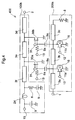
- FIG. 6 is a circuit diagram illustrating a bidirectional amplifier in accordance with a sixth embodiment of the present invention.
- a bidirectional amplifier 600 of this sixth embodiment comprises a distributed amplifier 600a including dual gate FETs 60a and 60b as amplifier FETs and two SPDT switches 500a and 500b each including two FETs 17a and 17b.
- first gates 61a and 61b and second gates 62a and 62b of the respective dual gates FETs 60a and 60b are connected to the input side circuits 100a shown in figure 1 via capacitors 9, and sources and drains of the respective dual gate FETs 60a and 60b are connected to the output side circuits 100b shown in figure 1.
- a first terminal 19a of the SPDT switch 500a is connected through a capacitor 9a to an output terminal 2c of the output side circuit 100b which is connected to the sources of the dual gate FETs 60a and 60b, and a second terminal 19b of the SPDT switch 500a is connected through a capacitor 9b to an input terminal 1c of the input side circuit 100a which is connected to the first gates 61a and 61b of the dual gate FETs 60a and 60b.
- a first terminal 19a of the SPDT switch 500b is connected through a capacitor 9b to an input terminal 1d of the input side circuit 100a which is connected to the second gates 62a and 62b of the dual gate FETs 60a and 60b, and a second terminal 19b of the SPDT switch 500b is connected through a capacitor 9b to an output terminal 2d of the output side circuit 100b which is connected to the drains of the dual gate FETs 60a and 60b.
- the FETs 17a of the SPDT switches 500a and 500b are turned off and the FETs 17b of these switches are turned on by the switching control gate bias applied to the terminals 18.
- the source-grounded FETs 11a and 11b of the input side circuit 100a connected to the first gates 61a and 61b are turned off by a gate bias applied thereto, i.e., the distributed switch is turned on, and on the contrary, the source-grounded FETs 11a and 11b of the input side circuit 100a connected to the second gates 62a and 62b are turned on by a gate bias applied thereto, i.e., the distributed switch is turned off.
- 0 V is applied to the drain bias terminal 15 of the output side circuit 100b which is connected to the sources of the dual gate FETs 60a and 60b to enable the FETs 7a and 7b of the output side circuits 100b to perform the switching operation, and a bias voltage to turn on the FETs 7a and 7b is applied to the gate bias terminals 13 of these FETs 7a and 7b to turn off the distributed constant lines 3d, 3e, and 3f of the output side circuit 100b.
- a signal is input to the input-output terminal 20a of the SPDT switch 500a from the outside, amplified in the input side circuit 100a connected to the first gates 61a and 61b and in the output side circuit 100b connected to the drains of the dual gate FETs, and output from the input-output terminal 20b of the SPDT switch 500b.
- a signal is input to the input-output terminal 20b of the SPDT switch 500b from the outside and amplified in the input side circuit 100a connected to the second gates 62a and 62b of the dual gate FETs 60a and 60b and in the output side circuit 100b connected to the sources of the dual gate FETs.
- the amplified signal is output from the input-output terminal 20a of the SPDT switch 500b.
- the bidirectional amplifier 600 according to the sixth embodiment of the present invention achieves the same amplification as that of the bidirectional amplifier 500 according to the fifth embodiment with the same effects as described above.
- the distributed amplifier includes two amplifier FETs, it may include three or more amplifier FETs with the same effects as described above.
Landscapes
- Engineering & Computer Science (AREA)
- Power Engineering (AREA)
- Microwave Amplifiers (AREA)
- Amplifiers (AREA)
Abstract
Description
- The present invention relates to a distributed amplifier and a bidirectional amplifier including the distributed amplifier.
- Figure 7 is a circuit diagram illustrating a structure of a prior art distributed amplifier. In figure 7, a
distributed amplifier 700 comprises aninput side circuit 70a disposed between an input terminal and ground, anoutput side circuit 70b disposed between anoutput terminal 2 and ground, and source-grounded FETs input circuit 70a and theoutput circuit 70b. Theinput side circuit 70a comprises three distributedconstant lines 3a to 3c, aterminal resistor 8 of 50 Ω, and abypass capacitor 9 which are connected in series between the input terminal 1 and ground. Theoutput side circuit 70b comprises three distributedconstant lines 3d to 3f, aterminal resistor 8 of 50 Ω, and abypass capacitor 9 which are connected in series between theoutput terminal 2 and ground. The source-grounded FET 70c includes a gate connected to the junction of the input side distributedconstant lines constant lines constant line 10. The source-grounded FET 70c includes a gate connected to the junction of the input side distributedconstant lines constant lines constant line 10. - Each of the source-grounded
FETs current supply 5 controlled by a gate bias voltage, and a drain-to-source capacitance 6. - In the
distributed amplifier 700, if the distributedconstant lines 3a to 3c of theinput side circuit 70a on the gate side of the source-grounded FET 70c (70d) is regarded as an inductance (Lg), the gate-source capacitance (Cgs) 4 of the FET and the inductance (Lg) form a circuit equivalent to a distributed constant line on the gate side of the FET. Similarly, if the distributedconstant line 10 connected to the drain of the source-grounded FET 70c (70d) is regarded as an inductance (Ld), the drain-source capacitance (Cds) 6 of the FET and the inductance (Ld) form a circuit equivalent to a distributed constant line on the drain side of the FET. - A description is given of the operation.
- Assuming that the input or output side characteristic impedance be Zo, the following equation (3) is achieved on the gate side of the source-grounded
FET 70c (70d).
In this case, the cut-off frequency fc is represented by
The same relationship as described above is achieved on the drain side of the FET. Further, the input signal is amplified by the FET. - As described above, this
distributed amplifier 700 is a broadband amplifier that can be used until the cut-off frequency. - When a Transmit/Receive (hereinafter referred to as T/R) module is fabricated using the prior art
distributed amplifier 700, twodistributed amplifiers 700 serving as a transmitter and a receiver, respectively, are required and, in addition, a T/R switch of a frequency band as wide as or wider than that of the distributed amplifier is required for switching the signal input-output path between the transmitter and the receiver. Therefore, if a T/R module is fabricated using the prior artdistributed amplifiers 700, the chip size of the T/R module is unfavorably increased by the T/R switch. Further, the signal transmission loss due to the T/R switch must be considered. -
- It is an object of the present invention to provide a distributed amplifier including a switch.
- It is another object of the present invention to provide a small-sized bidirectional amplifier.
- Other objects and advantages of the present invention will become apparent from the detailed description given hereinafter; it should be understood, however, that the detailed description and specific embodiment are given by way of illustration only, since various changes and modifications within the scope of the invention will become apparent to those skilled in the art from this detailed description.
- According to a first aspect of the present invention, a distributed amplifier comprises an input side circuit including a plurality of distributed constant lines connected in series between an input terminal and ground, and a plurality of source-grounded FETs for switching operation having drains connected to junctions between the distributed constant lines of the input side circuit; an output side circuit including a plurality of distributed constant lines connected in series between an output terminal and ground; and a plurality of source-grounded amplifier FETs each having a gate connected to the junction of the distributed constant lines of the input side circuit via a capacitor and a drain connected to the junction of the distributed constant lines of the output side circuit. In this structure, since the input side circuit also serves as a distributed switch, when a T/R module is fabricated using the distributed amplifier, no additional distributed switch for controlling signal input and output is needed, so that the chip size of the T/R module is reduced compared to the conventional T/R module. In addition, signal transmission loss is reduced.
- According to a second aspect of the present invention, a bidirectional amplifier comprises first and second distributed amplifiers of the same structure as described above, and first and second SPDT (single Pole Double Throw) switches each having first, second, and third terminals wherein an input signal applied to the first terminal is output from one of the second and third terminals, or one of two input signals respectively applied to the second and third terminals is output from the first terminal. One of the second and third terminals of the first SPDT switch is connected to an input terminal of the first distributed amplifier and the other is connected to an output terminal of the second distributed amplifier. One of the second and third terminals of the second SPDT switch is connected to an output terminal of the first distributed amplifier and the other is connected to an input terminal of the second distributed amplifier. The first terminals of the first and second SPDT switches are input-output terminals of the whole circuit. In this structure, since the bidirectional amplifier is fabricated using only two distributed amplifiers and two SPDT switches with no additional distributed switch, the chip size of the amplifier is reduced compared to the conventional bidirectional amplifier, and the signal transmission loss is reduced.
- According to a third aspect of the present invention, a bidirectional amplifier comprises first and second SPDT switches of the same structure as described above and a distributed amplifier. The distributed amplifier comprises a plurality of dual gate FETs for amplification each having first and second gates, a source, and a drain, first and second input side circuits of the same structure as described above respectively connected to the first gates and the second gates of the dual gate FETs, and first and second output side circuits of the same structure as described above respectively connected to the sources and the drains of the dual gate FETs. The second terminal of the first SPDT switch is connected to an input terminal of the first input side circuit, and the third terminal is connected to an output terminal of the first output side circuit. The second terminal of the second SPDT switch is connected to an input terminal of the second input side circuit, and the third terminal is connected to an output terminal of the second output side circuit. The first terminals of the first and second SPDT switches are input-output terminals of the whole circuit. In this structure, since the bidirectional amplifier is fabricated using only one distributed amplifier and two SPDT switches with no additional distributed switch, the chip size of the amplifier is reduced compared to the conventional bidirectional amplifier, and the signal transmission loss is reduced.
- Figure 1 is a circuit diagram illustrating a distributed amplifier in accordance with a first embodiment of the present invention.
- Figure 2 is a circuit diagram illustrating a distributed amplifier in accordance with a second embodiment of the present invention.
- Figure 3 is a circuit diagram illustrating a distributed amplifier in accordance with a third embodiment of the present invention.
- Figure 4 is a circuit diagram illustrating a distributed amplifier in accordance with a fourth embodiment of the present invention.
- Figure 5 is a circuit diagram illustrating a bidirectional amplifier in accordance with a fifth embodiment of the present invention.
- Figure 6 is a circuit diagram illustrating a bidirectional amplifier in accordance with a sixth embodiment of the present invention.
- Figure 7 is a circuit diagram illustrating a distributed amplifier in accordance with the prior art.
- Figure 1 is a circuit diagram illustrating a distributed amplifier in accordance with a first embodiment of the present invention. In figure 1, the same reference numerals as in figure 7 designate the same or corresponding parts. A
distributed amplifier 100 comprises aninput side circuit 100a disposed between an input terminal 1 and ground, anoutput side circuit 100b disposed between anoutput terminal 2 and ground, and source-grounded FETs input side circuit 100a and theoutput side circuit 100b. - The source-
grounded FETs capacitor 9a to the junction of the distributedconstant lines input side circuit 100a and a drain connected to the junction of the distributedconstant lines output side circuit 100b. Agate bias terminal 13 is connected through aresistor 8a to the junction of the gate of theFET 7a and thecapacitor 9a. The FET 7b includes a gate connected through acapacitor 9a to the junction of the distributedconstant lines input side circuit 100a and a drain connected to the junction of the distributedconstant lines output side circuit 100b. Agate bias terminal 13 is connected through aresistor 8a to the junction of the gate of theFET 7b and thecapacitor 9a. - The
input side circuit 100a includes three distributedconstant lines 3a to 3c and aterminal resistor 8 which are connected in series between the input terminal 1 and ground, and two source-groundedFETs grounded FET 11a is connected to the junction of the distributedconstant lines FET 11b is connected to the junction of the distributedconstant lines constant lines 3a to 3c and theFETs gate bias terminal 12 is connected to a gate of each FET. - The
output side circuit 100b includes three distributedconstant lines 3d to 3f, aterminal resistor 8, and abypass capacitor 9 which are connected in series between anoutput terminal 2 and ground. In addition, adrain bias terminal 15 for the source-grounded FETs RF choke coil 14 to the junction of theterminal resistor 8 and the distributedconstant line 3f, and abypass capacitor 9 is inserted between ground and the junction of thedrain bias terminal 15 and theRF choke coil 14. - A description is given of the operation.
- Since the source and the drain of the source-grounded
FET 11a (11b) are set at the same voltage by theterminal resistor 8, a switching operation is possible according to a bias voltage applied to thegate bias terminal 12. When the source-grounded FETs input side circuit 100a and thedistributed amplifier 100 operates similarly as the prior artdistributed amplifier 700. On the other hand, when the source-groundedFETs input side circuit 100a. - The source-grounded
FET 11a (11b) in the ON state has no resistance and the FET in the OFF state becomes a capacitance (CT). The capacitance (C) of thecapacitor 9 connected to the drain of theFET 11a (11b) has the relation of C >> CT,Cgs. - When the
FET amplifier 100 operates in the same manner as theprior art amplifier 700.
When theFETs input side circuit 100a. For this purpose, it is necessary to design theFETs capacitors 9 so that the respective parameters C, CT, and Cgs have the relation of

As described above, in the distributedamplifier 100 according to the first embodiment of the present invention, theinput side circuit 100a serves both as an amplifier and a switch for determining whether a signal is input to the distributedamplifier 100 or not. Therefore, when a T/R module is fabricated using this distributedamplifier 100, no additional distributed switch is needed, so that the chip size of the T/R module is reduced compared to the prior art. Further, it is not necessary to consider the signal transmission loss due to the distributed switch, so that the design of the T/R module is simplified. - Figure 2 is a circuit diagram illustrating a distributed amplifier in accordance with a second embodiment of the present invention. In figure 2, the same reference numerals as in figure 1 designate the same or corresponding parts. The structure of the distributed
amplifier 200 of this second embodiment is fundamentally identical to that of the first embodiment except that aninductor 16 is interposed between the source and the drain of each of the source-groundedFETs - Assuming that the inductance of the
inductor 16 be L, the working frequency (fo) is represented by
and if the inductance L of theinductor 16 is designed so that the working frequency fo is a desired value, this distributedamplifier 200 is available in a narrow band. - Figure 3 is a circuit diagram illustrating a distributed amplifier in accordance with a third embodiment of the present invention. In figure 3, the same reference numerals as in figure 1 designate the same or corresponding parts. A distributed
amplifier 300 of this third embodiment employsdual gate FETs FETs amplifier 100 of the first embodiment, and agate bias terminal 31 for controlling gain is connected to one of two gates of each dual gate FET. In this structure, since the gain of the amplifier is controlled by the bias voltage applied to thedual gate FETs - Figure 4 is a circuit diagram illustrating a distributed amplifier in accordance with a fourth embodiment of the present invention. In figure 4, the same reference numerals as those in figures 2 and 3 designate the same or corresponding parts. A distributed
amplifier 400 according to this fourth embodiment is fundamentally identical to the distributedamplifier 300 of the third embodiment except that theinput side circuit 200a of the second embodiment shown in figure 2 is employed in place of theinput side circuit 100a. - The distributed
amplifier 400 of this fourth embodiment provides the same effects as described in the third embodiment. In addition, theamplifier 400 can be used in a narrower band than the distributedamplifier 300 of the third embodiment. - Figure 5 is a circuit diagram illustrating a bidirectional amplifier in accordance with a fifth embodiment of the present invention. In the figure, the same reference numerals as those in figure 1 designate the same or corresponding parts. In this fifth embodiment, a
bidirectional amplifier 500 comprises two distributedamplifiers amplifier 100 according to the first embodiment, and two SPDT (Single Pole Double Throw) switches 500a and 500b each comprising twoFETs input terminal 1a of the distributedamplifier 100A is connected to afirst terminal 19a of theSPDT switch 500a via acapacitor 9b, and anoutput terminal 2b of the distributedamplifier 100B is connected to a second terminal 19b of theSPDT switch 500a via acapacitor 9b. Anoutput terminal 2a of the distributedamplifier 100A is connected to afirst terminal 19a of theSPDT switch 500b via acapacitor 9b, and aninput terminal 1b of the distributedamplifier 100B is connected to a second terminal 19b of theSPDT switch 500b via acapacitor 9b. -
Reference numerals numerals FETs 10a and 17b, and sources of these FETs are connected to ground viaresistors 8a.Reference numeral 18 designates a gate bias terminal for controlling the switching. - A description is given of the operation.
- First of all, the
FETs 17a of the SPDT switches 500a and 500b are turned on and the FETs 17b of these switches are turned off by the switching control gate bias applied to theterminals 18. The source-groundedFETs input side circuit 100a of the distributedamplifier 100A are turned off by the gate bias applied thereto, i.e., the distributed switch is turned on, and on the contrary, the source-groundedFETs amplifier 100B are turned on by the gate bias applied thereto, i.e., the distributed switch is turned off. Further, 0 V is applied to thedrain bias terminal 15 of the distributedamplifier 100B to enable theFETs amplifier 100B to perform the switching operation. A bias voltage to turn on theFETS gate bias terminals 13 of theFETs constant lines output terminal 20a. - In this case, a signal is input to the input-
output terminal 20a of theSPDT switch 500a from the outside, amplified in the distributedamplifier 100A, and output from the input-output terminal 20b of theSPDT switch 500b. - On the other hand, if the ON and OFF states of the respective FETs included in the distributed
amplifiers output terminal 20b of theSPDT switch 500b from the outside and amplified in the distributedamplifier 100B. The amplified signal is output from the input-output terminal 20a of theSPDT switch 500b. - As described above, differently from the prior art bidirectional amplifier, the
bidirectional amplifier 500 according to the fifth embodiment of the present invention does not require a supplemental distributed switch between the distributed amplifiers and the SPDT switches for preventing an adverse effect of the axial radiation generated in one of the distributed amplifiers through which no signal is transmitted on the other distributed amplifier through which signal is transmitted. Therefore, thebidirectional amplifier 500 is fabricated using only two distributed amplifiers and two SPDT switches, resulting in a reduction in the chip size compared to the conventional bidirectional amplifier. - Figure 6 is a circuit diagram illustrating a bidirectional amplifier in accordance with a sixth embodiment of the present invention. In figure 6, the same reference numerals as in figures 1 and 5 designate the same or corresponding parts. A
bidirectional amplifier 600 of this sixth embodiment comprises a distributedamplifier 600a includingdual gate FETs SPDT switches FETs amplifier 600a,first gates 61a and 61b andsecond gates dual gates FETs input side circuits 100a shown in figure 1 viacapacitors 9, and sources and drains of the respectivedual gate FETs output side circuits 100b shown in figure 1. Afirst terminal 19a of theSPDT switch 500a is connected through acapacitor 9a to anoutput terminal 2c of theoutput side circuit 100b which is connected to the sources of thedual gate FETs SPDT switch 500a is connected through acapacitor 9b to aninput terminal 1c of theinput side circuit 100a which is connected to thefirst gates 61a and 61b of thedual gate FETs first terminal 19a of theSPDT switch 500b is connected through acapacitor 9b to aninput terminal 1d of theinput side circuit 100a which is connected to thesecond gates dual gate FETs SPDT switch 500b is connected through acapacitor 9b to anoutput terminal 2d of theoutput side circuit 100b which is connected to the drains of thedual gate FETs - A description is given of the operation.
- First of all, the
FETs 17a of the SPDT switches 500a and 500b are turned off and the FETs 17b of these switches are turned on by the switching control gate bias applied to theterminals 18. In addition, the source-groundedFETs input side circuit 100a connected to thefirst gates 61a and 61b are turned off by a gate bias applied thereto, i.e., the distributed switch is turned on, and on the contrary, the source-groundedFETs input side circuit 100a connected to thesecond gates - Further, 0 V is applied to the
drain bias terminal 15 of theoutput side circuit 100b which is connected to the sources of thedual gate FETs FETs output side circuits 100b to perform the switching operation, and a bias voltage to turn on theFETs gate bias terminals 13 of theseFETs constant lines output side circuit 100b. - In this case, a signal is input to the input-
output terminal 20a of theSPDT switch 500a from the outside, amplified in theinput side circuit 100a connected to thefirst gates 61a and 61b and in theoutput side circuit 100b connected to the drains of the dual gate FETs, and output from the input-output terminal 20b of theSPDT switch 500b. - On the other hand, if the ON and OFF states of the respective FETs of the distributed
amplifier 600a and the respective FETS of the first andsecond SPDT switches output terminal 20b of theSPDT switch 500b from the outside and amplified in theinput side circuit 100a connected to thesecond gates dual gate FETs output side circuit 100b connected to the sources of the dual gate FETs. The amplified signal is output from the input-output terminal 20a of theSPDT switch 500b. - The
bidirectional amplifier 600 according to the sixth embodiment of the present invention achieves the same amplification as that of thebidirectional amplifier 500 according to the fifth embodiment with the same effects as described above. - While in the above-described first to sixth embodiments the distributed amplifier includes two amplifier FETs, it may include three or more amplifier FETs with the same effects as described above.
Claims (8)
- A distributed amplifier (100) (Fig. 1) comprising:
an input side circuit (100a) including a plurality of distributed constant lines (3a,3b,3c) connected in series between an input terminal (1) and ground, and a plurality of source-grounded FETs (11a,11b) for switching operation having drains connected to junctions between said distributed constant lines (3a,3b,3c);
an output side circuit (100b) including a plurality of distributed constant lines (3d,3e,3f) connected in series between an output terminal (15) and ground; and
a plurality of source-grounded amplifier FETs (7a,7b) having gates connected to junctions between said distributed constant lines (3a,3b,3c) of said input side circuit (100a) via capacitors (9a) and drains connected to junctions of said distributed constant lines (3d,3e,3f) of said output side circuit (100b). - The distributed amplifier of claim 1 wherein said capacitors (9a) and said source-grounded FETs (11a,11b) for switching are designed to satisfy the following relations (1) and (2):


- A distributed amplifier as defined in claim 1 or 2 (Fig.2) further including an inductor (16) interposed between source and drain of said source-grounded FET (11a,11b) for switching operation.
- A distributed amplifier as defined in claim 1 or 2 (Fig.3) wherein said amplifier FET (7a,7b) is a dual gate FET having two gates and a bias voltage for controlling gain is applied to one of said two gates.
- A bidirectional amplifier (500) (Fig.5) comprising:
first and second distributed amplifiers (100A,100B) each comprising an input side circuit (100a) including a plurality of distributed constant lines (3a,3b,3c) connected in series between an input terminal (1a,1b) and ground and a plurality of source-grounded FETs (11a,11b) for switching operation having drains connected to junctions between said distributed constant lines (3a,3b,3c), an output side circuit (100b) including a plurality of distributed constant lines (3d,3e,3f) connected in series between an output terminal (2a,2b) and ground, and a plurality of source-grounded amplifier FETs (7a,7b) having gates connected to junctions between said distributed constant lines (3a,3b,3c) of said input side circuit (100a) via capacitors (9a) and drains connected to junctions of said distributed constant lines (3d,3e,3f) of said output side circuit (100b);
first and second SPDT (Single Pole Double Throw) switches (500a,500b) each having first, second, and third terminals (20a or 20b, 19a, 19b) wherein an input signal applied to said first terminal (20a) is output from one of said second and third terminals (19a,19b), or one of two input signals respectively input to said second and third terminals (19a,19b) is output from said first terminal (20b);
one of said second and third terminals (19a,19b) of said first SPDT switch (500a) being connected to an input terminal (1a) of said first distributed amplifier (100A) and the other being connected to an output terminal (19b) of said second distributed amplifier (100B);
one of said second and third terminals (19a,19b) of said second SPDT switch (500b) being connected to an output terminal (2a) of said first distributed amplifier (100A) and the other being connected to an input terminal (1b) of said second distributed amplifier (100B); and
said first terminals (20a,20b) of said first and second SPDT switches (500a,500b) being input-output terminals of the whole circuit. - A bidirectional amplifier (600) (Fig.6) comprising:
a distributed amplifier (600a) comprising first and second input side circuits (100a) each comprising a plurality of distributed constant lines (3a,3b,3c) connected in series between an input terminal (1c,1d) and ground and a plurality of source-grounded FETs (11a,11b) for switching operation having drains connected to junctions between said distributed constant lines (3a,3b,3c), first and second output side circuits (100b) each comprising a plurality of distributed constant lines (3d,3e,3f) connected between an output terminal (2c,2d) and ground, and a plurality of dual gate FETs (60a,60b) for amplification each having first and second gates (61a,61b,62a,62b), a source, and a drain, said first gate being connected through a capacitor (9) to the junction between said distributed constant lines (3a,3b,3c) of said first input side circuit (100a) while the other being connected through a capacitor (9) to the junction between said distributed constant lines (3a,3b,3c) of said second input side circuit (100a), and one of said source and drain being connected to the junction of said distributed constant lines (3d,3e,3f) of said first output side circuit (100b) while the other being connected to the junction of said distributed constant lines (3d,3e,3f) of said second output side circuit (100b);
first and second SPDT switches (500a,500b) each having first, second, and third terminals (20a or 20b,19a,19b) wherein an input signal applied to said first terminal (20a) is output from one of said second and third terminals (19a,19b), or one of two input signals respectively applied to said second and third terminals (19a,19b) is output from said first terminal (20b);
said second terminal (19a) of said first SPDT switch (500a) being connected to an output terminal (2c) of said first output side circuit (100b) and said third terminal (19b) being connected to an input terminal (1c) of said first input side circuit (100a);
said second terminal (19a) of said second SPDT switch (500b) being connected to an input terminal (1d) of said second input side circuit (100a) and said third terminal (19b) being connected to an output terminal (2d) of said second output side circuit (100b); and
said first terminals (20a,20b) of said first and second SPDT switches (500a,500b) being input-output terminals of the whole circuit. - A bidirectional amplifier as defined in claim 5 or 6 further comprising a drain bias terminal (15) for controlling drain bias of each amplifier FET (7a,7b), disposed in said output side circuit (100b).
- A bidirectional amplifier as defined in claim 5 or 6 wherein said source-grounded FETs (11a,11b) for switching operation and said capacitors (9a) are designed to satisfy the following relations (1) and (2):

Applications Claiming Priority (2)
| Application Number | Priority Date | Filing Date | Title |
|---|---|---|---|
| JP5173907A JPH0730343A (en) | 1993-07-14 | 1993-07-14 | Distributed amplifier and bidirectional amplifier |
| JP173907/93 | 1993-07-14 |
Publications (2)
| Publication Number | Publication Date |
|---|---|
| EP0634836A2 true EP0634836A2 (en) | 1995-01-18 |
| EP0634836A3 EP0634836A3 (en) | 1997-11-19 |
Family
ID=15969297
Family Applications (1)
| Application Number | Title | Priority Date | Filing Date |
|---|---|---|---|
| EP94109213A Withdrawn EP0634836A3 (en) | 1993-07-14 | 1994-06-15 | Distributed amplifier and bidirectional amplifier |
Country Status (3)
| Country | Link |
|---|---|
| US (1) | US5414387A (en) |
| EP (1) | EP0634836A3 (en) |
| JP (1) | JPH0730343A (en) |
Cited By (2)
| Publication number | Priority date | Publication date | Assignee | Title |
|---|---|---|---|---|
| WO2002075921A3 (en) * | 2001-03-15 | 2003-12-11 | Motorola Inc | Distributed amplifier having separately biased sections |
| US7239852B2 (en) * | 2003-08-01 | 2007-07-03 | Northrop Grumman Corporation | Asymmetric, optimized common-source bi-directional amplifier |
Families Citing this family (29)
| Publication number | Priority date | Publication date | Assignee | Title |
|---|---|---|---|---|
| DE2239942C3 (en) * | 1972-08-14 | 1988-02-11 | Wacker-Chemie GmbH, 8000 München | Process for the polymerization of vinyl chloride |
| US6049250A (en) * | 1998-04-03 | 2000-04-11 | Trw Inc. | Dittributed feed back distributed amplifier |
| US6008694A (en) * | 1998-07-10 | 1999-12-28 | National Scientific Corp. | Distributed amplifier and method therefor |
| JP3951495B2 (en) | 1999-03-18 | 2007-08-01 | 株式会社日立製作所 | Traveling wave power combining circuit and radio base station |
| GB2373937A (en) * | 2001-03-27 | 2002-10-02 | Secr Defence | Improvements in travelling wave amplifiers |
| US6650200B2 (en) * | 2001-04-20 | 2003-11-18 | Anaren Microwave, Inc. | Dynamic combiner/splitter for RF signal systems |
| WO2003065572A1 (en) * | 2002-01-25 | 2003-08-07 | Centellax, Inc. | Distributed level-shifting network for cascading broadband amplifiers |
| US8669812B2 (en) * | 2004-11-23 | 2014-03-11 | Schilmass Co., L.L.C. | High power amplifier |
| US8076975B1 (en) | 2004-11-23 | 2011-12-13 | Bae Systems Information And Electronic Systems Integration Inc. | Broadband high power amplifier |
| US7733185B2 (en) * | 2005-10-24 | 2010-06-08 | Nec Corporation | Distributed amplifier and integrated circuit |
| US8035449B1 (en) * | 2009-01-02 | 2011-10-11 | Rf Micro Devices, Inc. | Capacitively-coupled distributed amplifier with baseband performance |
| JP5764742B2 (en) * | 2010-05-17 | 2015-08-19 | パナソニックIpマネジメント株式会社 | Junction field effect transistor, method of manufacturing the same, and analog circuit |
| US8665022B2 (en) | 2011-04-28 | 2014-03-04 | Rf Micro Devices, Inc. | Low noise-linear power distributed amplifier |
| US8823455B2 (en) | 2011-09-13 | 2014-09-02 | Rf Micro Devices, Inc. | Matrix distributed power amplifier |
| US9093420B2 (en) | 2012-04-18 | 2015-07-28 | Rf Micro Devices, Inc. | Methods for fabricating high voltage field effect transistor finger terminations |
| US9124221B2 (en) | 2012-07-16 | 2015-09-01 | Rf Micro Devices, Inc. | Wide bandwidth radio frequency amplier having dual gate transistors |
| US9202874B2 (en) | 2012-08-24 | 2015-12-01 | Rf Micro Devices, Inc. | Gallium nitride (GaN) device with leakage current-based over-voltage protection |
| US9147632B2 (en) | 2012-08-24 | 2015-09-29 | Rf Micro Devices, Inc. | Semiconductor device having improved heat dissipation |
| US9142620B2 (en) | 2012-08-24 | 2015-09-22 | Rf Micro Devices, Inc. | Power device packaging having backmetals couple the plurality of bond pads to the die backside |
| US8988097B2 (en) | 2012-08-24 | 2015-03-24 | Rf Micro Devices, Inc. | Method for on-wafer high voltage testing of semiconductor devices |
| US9917080B2 (en) | 2012-08-24 | 2018-03-13 | Qorvo US. Inc. | Semiconductor device with electrical overstress (EOS) protection |
| US9070761B2 (en) | 2012-08-27 | 2015-06-30 | Rf Micro Devices, Inc. | Field effect transistor (FET) having fingers with rippled edges |
| WO2014035794A1 (en) | 2012-08-27 | 2014-03-06 | Rf Micro Devices, Inc | Lateral semiconductor device with vertical breakdown region |
| US9325281B2 (en) | 2012-10-30 | 2016-04-26 | Rf Micro Devices, Inc. | Power amplifier controller |
| US9455327B2 (en) | 2014-06-06 | 2016-09-27 | Qorvo Us, Inc. | Schottky gated transistor with interfacial layer |
| US9536803B2 (en) | 2014-09-05 | 2017-01-03 | Qorvo Us, Inc. | Integrated power module with improved isolation and thermal conductivity |
| US10615158B2 (en) | 2015-02-04 | 2020-04-07 | Qorvo Us, Inc. | Transition frequency multiplier semiconductor device |
| US10062684B2 (en) | 2015-02-04 | 2018-08-28 | Qorvo Us, Inc. | Transition frequency multiplier semiconductor device |
| WO2025224848A1 (en) * | 2024-04-24 | 2025-10-30 | 三菱電機株式会社 | Distributed amplifier |
Family Cites Families (7)
| Publication number | Priority date | Publication date | Assignee | Title |
|---|---|---|---|---|
| US4918401A (en) * | 1985-09-30 | 1990-04-17 | Siemens Aktiengesellschaft | Step adjustable distributed amplifier network structure |
| US5081706A (en) * | 1987-07-30 | 1992-01-14 | Texas Instruments Incorporated | Broadband merged switch |
| JPH01205458A (en) * | 1988-02-10 | 1989-08-17 | Matsushita Electron Corp | Monolithic microwave integrated circuit |
| US4973918A (en) * | 1988-12-27 | 1990-11-27 | Raytheon Company | Distributed amplifying switch/r.f. signal splitter |
| US4983865A (en) * | 1989-01-25 | 1991-01-08 | Pacific Monolithics | High speed switch matrix |
| JPH0349401A (en) * | 1989-07-18 | 1991-03-04 | Mitsubishi Electric Corp | Microwave element |
| US5046155A (en) * | 1990-04-06 | 1991-09-03 | Wisconsin Alumni Research Foundation | Highly directive, broadband, bidirectional distributed amplifier |
-
1993
- 1993-07-14 JP JP5173907A patent/JPH0730343A/en active Pending
-
1994
- 1994-06-13 US US08/258,831 patent/US5414387A/en not_active Expired - Fee Related
- 1994-06-15 EP EP94109213A patent/EP0634836A3/en not_active Withdrawn
Cited By (2)
| Publication number | Priority date | Publication date | Assignee | Title |
|---|---|---|---|---|
| WO2002075921A3 (en) * | 2001-03-15 | 2003-12-11 | Motorola Inc | Distributed amplifier having separately biased sections |
| US7239852B2 (en) * | 2003-08-01 | 2007-07-03 | Northrop Grumman Corporation | Asymmetric, optimized common-source bi-directional amplifier |
Also Published As
| Publication number | Publication date |
|---|---|
| US5414387A (en) | 1995-05-09 |
| JPH0730343A (en) | 1995-01-31 |
| EP0634836A3 (en) | 1997-11-19 |
Similar Documents
| Publication | Publication Date | Title |
|---|---|---|
| EP0634836A2 (en) | Distributed amplifier and bidirectional amplifier | |
| JP2964975B2 (en) | High frequency switch circuit | |
| EP0854570B1 (en) | Bias stabilizing circuit | |
| US6066993A (en) | Duplexer circuit apparatus provided with amplifier and impedance matching inductor | |
| US5903178A (en) | Semiconductor integrated circuit | |
| EP0622894B1 (en) | Semiconductor power amplifier integrated circuit | |
| JPH0927736A (en) | FET switch | |
| US20030058041A1 (en) | Variable gain amplifier | |
| US5694085A (en) | High-power amplifier using parallel transistors | |
| JP4570339B2 (en) | Ultra-wideband distributed amplifier with active loading device for bias application | |
| US5675290A (en) | Microwave amplifier circuit | |
| KR100471157B1 (en) | Antenna switching module having amplification function | |
| EP1169776B1 (en) | Biasing arrangement for field effect transistors | |
| US5087893A (en) | RF driven gate bias | |
| US5057791A (en) | Device and method for bi-directional amplification with a JFET | |
| US20070069798A1 (en) | Switch circuit for high-frequency-signal switching | |
| US6104247A (en) | Power amplifier for mobile communication system | |
| JPH06232657A (en) | High frequency amplifier | |
| KR100375520B1 (en) | Linearizer | |
| JP3250693B2 (en) | Output switching amplifier | |
| KR102800425B1 (en) | Ultra high frequency amplifier | |
| JP2001160724A (en) | Amplifier with switch | |
| JPH0473805B2 (en) | ||
| JPH10190380A (en) | Amplifier with switch | |
| JPH06101653B2 (en) | Monolithic microwave amplifier |
Legal Events
| Date | Code | Title | Description |
|---|---|---|---|
| PUAI | Public reference made under article 153(3) epc to a published international application that has entered the european phase |
Free format text: ORIGINAL CODE: 0009012 |
|
| AK | Designated contracting states |
Kind code of ref document: A2 Designated state(s): DE FR GB |
|
| PUAL | Search report despatched |
Free format text: ORIGINAL CODE: 0009013 |
|
| AK | Designated contracting states |
Kind code of ref document: A3 Designated state(s): DE FR GB |
|
| 17P | Request for examination filed |
Effective date: 19980109 |
|
| 17Q | First examination report despatched |
Effective date: 20000713 |
|
| STAA | Information on the status of an ep patent application or granted ep patent |
Free format text: STATUS: THE APPLICATION IS DEEMED TO BE WITHDRAWN |
|
| 18D | Application deemed to be withdrawn |
Effective date: 20001124 |