EP0632560A2 - Semiconductor integrated circuit device equipped with protective system for directly discharging surge voltage from pad to discharging line - Google Patents
Semiconductor integrated circuit device equipped with protective system for directly discharging surge voltage from pad to discharging line Download PDFInfo
- Publication number
- EP0632560A2 EP0632560A2 EP94110025A EP94110025A EP0632560A2 EP 0632560 A2 EP0632560 A2 EP 0632560A2 EP 94110025 A EP94110025 A EP 94110025A EP 94110025 A EP94110025 A EP 94110025A EP 0632560 A2 EP0632560 A2 EP 0632560A2
- Authority
- EP
- European Patent Office
- Prior art keywords
- power supply
- port
- voltage
- supply port
- output
- Prior art date
- Legal status (The legal status is an assumption and is not a legal conclusion. Google has not performed a legal analysis and makes no representation as to the accuracy of the status listed.)
- Granted
Links
- 239000004065 semiconductor Substances 0.000 title claims abstract description 55
- 238000007599 discharging Methods 0.000 title claims abstract description 52
- 230000001681 protective effect Effects 0.000 title claims abstract description 44
- 239000012535 impurity Substances 0.000 claims description 13
- 239000000872 buffer Substances 0.000 description 35
- 238000010586 diagram Methods 0.000 description 5
- 239000000758 substrate Substances 0.000 description 5
- 230000005669 field effect Effects 0.000 description 4
- XAGFODPZIPBFFR-UHFFFAOYSA-N aluminium Chemical compound [Al] XAGFODPZIPBFFR-UHFFFAOYSA-N 0.000 description 3
- 229910052782 aluminium Inorganic materials 0.000 description 3
- 230000006378 damage Effects 0.000 description 3
- 230000003071 parasitic effect Effects 0.000 description 3
- XUIMIQQOPSSXEZ-UHFFFAOYSA-N Silicon Chemical compound [Si] XUIMIQQOPSSXEZ-UHFFFAOYSA-N 0.000 description 2
- 230000015556 catabolic process Effects 0.000 description 2
- 230000000295 complement effect Effects 0.000 description 2
- 238000000034 method Methods 0.000 description 2
- 230000001902 propagating effect Effects 0.000 description 2
- 229910052710 silicon Inorganic materials 0.000 description 2
- 239000010703 silicon Substances 0.000 description 2
- 230000007423 decrease Effects 0.000 description 1
- 230000003247 decreasing effect Effects 0.000 description 1
- 230000000694 effects Effects 0.000 description 1
- 238000012986 modification Methods 0.000 description 1
- 230000004048 modification Effects 0.000 description 1
- 230000002093 peripheral effect Effects 0.000 description 1
Images


Classifications
-
- H—ELECTRICITY
- H02—GENERATION; CONVERSION OR DISTRIBUTION OF ELECTRIC POWER
- H02H—EMERGENCY PROTECTIVE CIRCUIT ARRANGEMENTS
- H02H9/00—Emergency protective circuit arrangements for limiting excess current or voltage without disconnection
- H02H9/04—Emergency protective circuit arrangements for limiting excess current or voltage without disconnection responsive to excess voltage
- H02H9/045—Emergency protective circuit arrangements for limiting excess current or voltage without disconnection responsive to excess voltage adapted to a particular application and not provided for elsewhere
- H02H9/046—Emergency protective circuit arrangements for limiting excess current or voltage without disconnection responsive to excess voltage adapted to a particular application and not provided for elsewhere responsive to excess voltage appearing at terminals of integrated circuits
-
- H—ELECTRICITY
- H01—ELECTRIC ELEMENTS
- H01L—SEMICONDUCTOR DEVICES NOT COVERED BY CLASS H10
- H01L27/00—Devices consisting of a plurality of semiconductor or other solid-state components formed in or on a common substrate
- H01L27/02—Devices consisting of a plurality of semiconductor or other solid-state components formed in or on a common substrate including semiconductor components specially adapted for rectifying, oscillating, amplifying or switching and having at least one potential-jump barrier or surface barrier; including integrated passive circuit elements with at least one potential-jump barrier or surface barrier
- H01L27/04—Devices consisting of a plurality of semiconductor or other solid-state components formed in or on a common substrate including semiconductor components specially adapted for rectifying, oscillating, amplifying or switching and having at least one potential-jump barrier or surface barrier; including integrated passive circuit elements with at least one potential-jump barrier or surface barrier the substrate being a semiconductor body
-
- H—ELECTRICITY
- H01—ELECTRIC ELEMENTS
- H01L—SEMICONDUCTOR DEVICES NOT COVERED BY CLASS H10
- H01L27/00—Devices consisting of a plurality of semiconductor or other solid-state components formed in or on a common substrate
- H01L27/02—Devices consisting of a plurality of semiconductor or other solid-state components formed in or on a common substrate including semiconductor components specially adapted for rectifying, oscillating, amplifying or switching and having at least one potential-jump barrier or surface barrier; including integrated passive circuit elements with at least one potential-jump barrier or surface barrier
- H01L27/0203—Particular design considerations for integrated circuits
- H01L27/0248—Particular design considerations for integrated circuits for electrical or thermal protection, e.g. electrostatic discharge [ESD] protection
- H01L27/0251—Particular design considerations for integrated circuits for electrical or thermal protection, e.g. electrostatic discharge [ESD] protection for MOS devices
Definitions
- This invention relates to a semiconductor integrated circuit device and, more particularly, to a semiconductor integrated circuit device with a protective system against electrostatic destruction.
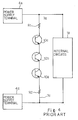
- a typical example of the protective system is disclosed in Japanese Patent Publication of Unexamined Application No. 3-72666, and figure 6 illustrates a schematic layout of a prior art semiconductor integrated circuit device with the protective system.
- a main circuit block 1 is assigned to internal circuits 1a of the integrated circuit, and circuit blocks 2 and 3 are assigned to output buffers 2a and 3a.
- the main circuit block occupies most of the real estate of a semiconductor chip where the integrated circuit is fabricated.
- the internal circuits are powered through a power supply terminal 4a and a ground terminal 5a, and an input signal is supplied from an input terminal 6a to the internal circuits 1a.
- the output buffers 2a and 3a are powered through respective power supply terminals 4b and 4c and respective ground terminals 5a and 5b, and output data signals are supplied from the internal circuits 1a through the output buffers 2a and 3a to respective output terminals 6b and 6c.
- FIG. 2 illustrates the prior art protection system incorporated in the semiconductor integrated circuit device shown in figure 1.
- a power supply line 7a is looped for propagating the power voltage Vcc to the internal circuits 1a, and is connected with the power supply terminal 4a.
- An earth line 8a is also looped for discharging current to the ground terminal 5a, and the power supply line 7a and the earth line 8a are hatched in opposite directions for the sake of clear discrimination.
- a power supply line 7b and an earth line 8b extend from the power supply terminal 4b and the ground terminal 5b in the circuit block 2 so as to power the output buffer 2a, and the other output buffer 3a is powered through a power supply line 7c and an earth line 8c respectively connected with the power supply terminal 4c and the ground terminal 5c.
- the power supply lines 7b and 7c are dotted for the sake of clear discrimination.
- the prior art protective system comprises a plurality of switching transistors 9a to 9v, and these switching transistors 9a to 9v discharge surge voltage or excess voltage to the earth line 8a and the power supply line 7a. For example, if the surge voltage over the potential at the ground terminal 5a is applied to the output terminal 6b, the switching transistor 9b turns on for discharging surge current to the earth line 8b, and, thereafter, the switching transistors 9q and 9r turn on for further discharging the surge current to the earth line 8a. For this reason, the surge current is finally discharged to the ground terminal 5a.
- the switching transistors 9s and 9t turn on for transferring the surge current from the power supply line 7c to the power supply line 8c, and, thereafter, the switching transistors 9u and 9v turn on for transferring the surge current from the earth line 8c to the earth line 8a.
- the switching transistors 9d to 9n turn on for discharging the surge current from the earth line 8a to the power supply line 7a, and the surge current is relayed to the power supply terminal 4a.
- FIG 3 illustrates the concept of the prior art protective system used for discharging the surge voltage applied to the power supply terminal 4c.
- the switching transistors 9s/9t, the switching transistors 9u/9v and the switching transistors 9d/9e/9f/9g/9h/9i/9j/9k/9m/9n are respectively represented by bipolar transistors 10a, 10b and 10c, because parasitic bipolar actions of the switching transistors 9s/9t, 9u/9v and 9d to 9n are used for clamping the associated power supply/earth lines at lower voltages than the serge voltage thereon.
- the prior art protective system discharges the surge current through the earth line 8a at all times, and the switching transistors 9a to 9v are arranged in such a manner as to allow the surge current to flow through the earth line 8a.
- the clamp voltage at each stage 10a, 10b or 10c is of the order of 7 volts, and the total potential difference is estimated at 21 volts.
- the large potential difference is applied across the gate oxide films of component MOS (Metal-Oxide-Semiconductor) transistors incorporated in the internal circuits 1a, and is much larger than the breakdown voltage of the gate oxide films as thin as 160 angstroms.
- MOS Metal-Oxide-Semiconductor
- Another problem inherent in the prior art protective system is a trade-off between the effect against the surge voltage and the semiconductor chip size. If the switching transistors 9s/9t, 9u/9v and 9d to 9n are decreased to the switching transistors 9s, 9v and 9d, by way of example, the resistances R1 and R2 shown in figure 4 are increased, and the prior art protective system can not rapidly discharge the surge current. On the other hand, if the switching transistors coupled in parallel are increased, the surge current is rapidly discharged. However, the switching transistors occupy a large amount of real estate, and the manufacturer needs to enlarge the semiconductor chip.
- the present invention proposes to directly discharge a surge current to a shared discharging line.
- a semiconductor integrated circuit device fabricated on a semiconductor chip, comprising: a) a main circuit having an input port for receiving an input signal, and responsive to the input signal for producing an output signal; b) an output circuit having an output port for transferring the output signal to the outside of the semiconductor integrated circuit device; c) a power supply system having a first power supply sub-system for supplying a first power voltage and a second power voltage to the main circuit and a second power supply sub-system for supplying the first power voltage and the second power voltage to the output circuit, the first power supply sub-system having a first power supply port supplied with the first power voltage and a second power supply port supplied with the second power voltage, the second power supply sub-system having a third power supply port supplied with the first power voltage and a fourth power supply port supplied with the second power voltage, the first power supply port and the second power supply port being electrically isolated from the third power supply port and the fourth power supply port, the semiconductor chip being biased with the second power voltage; and d)
- a semiconductor integrated circuit device embodying the present invention is fabricated on a single semiconductor chip 11, and the ground voltage biases the semiconductor chip 11 .
- the semiconductor integrated circuit device largely comprises an input buffer circuit 12, internal circuits 13, an output buffer circuit 14, a power supply system 15 and a protective system 16.
- An input signal pad 12a is electrically connected with the input buffer circuit 12, and the input buffer circuit 12 temporally stores the input signal.
- the input signal is relayed to the internal circuits 13.
- the input buffer circuit 12 is implemented by a series of a complementary inverter, i.e., a series of p-channel enhancement type switching transistor 12b and an n-channel enhancement type switching transistor 12c.
- the internal circuits 12 is operative to carry out a predetermined function on the input signals for producing an output signal, and the output signal is supplied from the internal circuits 12 to the output buffer circuit 14.
- the input buffer circuit 12 is illustrated in figure 5, other input signals are also supplied from input signal pads (not shown) through input buffer circuits (not shown) to the internal circuits, and the input pads and the input buffer circuits are similar to the input signal pad 12a and the input buffer circuits 12.
- the input signal pad 12a and the other input signal pads (not shown) form in combination an input signal port, and the input buffer circuit 12 and the other input buffer circuits (not shown) as a whole constitute an input buffer unit.
- the output buffer circuit 14 is also implemented by a complementary inverter, i.e., a series of a p-channel enhancement type switching transistor 14a and an n-channel enhancement type switching transistor 14b, and temporally stores the output signal.
- the output buffer circuit 14 is coupled with an output signal pad 14c, and the output signal is transferred from the output buffer circuit 14 through the output signal pad 14c to the outside of the semiconductor integrated circuit device.
- the power supply system 15 is broken down into two power supply sub-system 15a and 15b.
- the first power supply sub-system 15a comprises a power supply pad 15c supplied with a power voltage Vcc from the outside of the semiconductor chip 11, a power supply line 15d for distributing the power voltage Vcc to the input buffer circuit 12, the other input buffer circuits (not shown) and the internal circuits 13, a ground pad 15e for the ground voltage, a ground voltage line 15f shared between the input buffer circuit 12, the other input buffer circuits (not shown) and the internal circuits 13, an additional ground line 15g connected between the internal circuits 13 and an additional ground pad 15h and exclusively used by the internal circuits 13.
- the input buffer circuit 12, the other input buffer circuits and the internal circuits 13 are powered by the first power supply sub-system 15a, and the input buffer unit including the circuit 12 and the internal circuits 13 as a whole constitute a main circuit.
- the second power supply sub-system 15b comprises a power supply pad 15i supplied with the power voltage Vcc, a power supply line 15j for propagating the power voltage Vcc to the output buffer circuit 14, a ground pad 15k for the ground voltage and a ground voltage line 15m assigned to the output buffer circuit 14.
- the second power supply sub-system 15b is independent from the first power supply sub-system 15a, and the main circuit is electrically isolated from the output buffer circuit 14, because the output buffer circuit 14 expected to drive a large amount of current is causative of undesirable voltage fluctuation.
- the output buffer circuit 14 and the output signal pad 14c serve as an output circuit and an output signal port.
- Another semiconductor integrated circuit device may have more than one output buffer circuits respectively associated with output signal pads as shown in figure 6. If so, the plurality of output signal pads and the output buffer circuits form the output signal port and the output circuit, respectively.
- the protective system 16 comprises a shared discharging line 16a, an array 16b of protective units 16c, 16d, 16e, 16f, 16g, 16h,... and an input protection circuit 16i.
- the shared discharging line 16a is connected through the array 16b with the pads 15c, 12a, 15i, 14c, 15k, ..., and is directly connected with the ground pads 15e and 15h.
- the shared discharging line 16a extends along the outermost peripheral area partially in scribe lines (see figures 6 and 7), and a scribe wiring held in contact with the semiconductor chip 11 serves as the shared discharging.
- the pads 15c, 12a, 15e, 15i, 14c, 15k, 15h,... are arranged in the vicinity of the scribe wiring.
- the scribe wiring is usually incorporated in any kind of semiconductor integrated circuit device, and keeps the semiconductor chip 11 or the semiconductor substrate at a constant voltage (see figure 8).
- the scribe wiring 16a extends partially on an inter-level insulating layer 21 laminated on a thick field oxide layer 22, and is partially held in contact with a heavily doped p-type contact region 11a for forming an ohmic contact with the semiconductor chip 11.
- the shared discharging line 16a thus implemented by the scribe wirings does not increase the semiconductor chip size, nor makes the process sequence complex.
- the scribe wiring minimizes the length of the shared discharging line 16a, and a scribe wiring of aluminum is of the order of 3 ohms.
- each of the protective units 16c to 16h has a diode D and a clamping element CL coupled in parallel between the shared discharging line 16a and the associated pad. While no surge voltage is applied to the pads 15c, 12a, 15i, 14c, 15k, ...., the diodes D electrically isolate the pads from the shared discharging line 16a, and the pads are maintained at standard voltage levels such as the power voltage line Vcc, the ground voltage level and the input signal voltage. On the other hand, if surge voltage is applied to one of the pads, the clamping element CL discharges the surge current from the pad to the shared discharging line 16a.
- the diode D is implemented by a heavily-doped p-type impurity region 11b/the p-type silicon substrate 11 and a heavily-doped n-type impurity region 11c, and the heavily-doped p-type impurity region 11b/the p-type silicon substrate 11 serve as an anode of the diode D.
- the heavily-doped n-type impurity region 11c, the p-type semiconductor substrate 11 and a heavily-doped n-type impurity region 11d form in combination a lateral bipolar transistor serving as the clamping element CL.
- the heavily-doped n-type impurity region 11c is connected with an aluminum wiring 23 with the associated pad, and the heavily-doped p-type impurity region 11b and the heavily-doped n-type impurity region 11d are connected with a bifurcated aluminum wiring 24 merged into the scribe wiring 16a.
- the input protective circuit 16i comprises a resistor 16j and a discharging transistor 16k.
- the resistor 16j introduces time delay into the propagation of the surge voltage applied to the input signal pad 12a, and the discharging transistor 16k turns on in the presence of the surge voltage for directly discharging the surge current to the ground pad 15e.
- the clamping element may be implemented by a parasitic bipolar transistor of a MOS transistor, and the MOS transistor may be fabricated through a known CMOS process under 0.6-micron design rules. If so, the clamp voltage is of the order of 7 volts, and the build-in potential of the diode D is about 0.9 volt.
- the positive surge voltage is discharged from the input signal pad 12a through the clamping element CL of the protective unit 16d to the shared discharging line 16a, and is, in turn, supplied from the shared discharging line 16a through the diode D of the protective unit 16x.
- the positive surge voltage is applied to the input signal pad 12x, the positive surge voltage is discharged through the clamping element CL of the protective unit 16x to the shared discharging line 16a, and is, in turn, supplied from the shared discharging line 16a through the diode D of the protective unit 16d to the input signal pad 12a.
- the positive surge voltage When the positive surge voltage is applied to the input signal pad 12a, the positive surge voltage is discharged through the clamping element CL of the protective unit 16d to the shared discharging line 16a, and the shared discharging line 16a directly supplies the surge voltage to the ground pad 15e.
- the surge voltage passes through only one clamping element CL and only one diode D or through only one clamping element Cl or only one diode D, and small potential difference is merely applied to a gate insulating film of a component field effect transistor forming a part of the main circuit.
- the maximum potential difference is the total of the clamping voltage of the clamping element CL, the built-in potential of the diode D and the resistance of the shared discharging line 16a.
- the clamping voltage is about 7 volts, and the built-in potential is about 0.9 volt.
- the maximum resistance of the shared discharging line 16a is only 3 ohms, and the shared discharging line 16a steps down the voltage level therealong by only 3 volts against a peak surge current of 1 ampere. Therefore, the maximum potential difference is about 12 volts, and is smaller than the breakdown voltage of the gate insulating film equal to or greater than 100 angstroms.
- the protective system according to the present invention is effective against the surge voltage, and the component field effect transistors are never broken down.
- the protective system 16 is further effective against electrostatic charge at the package (not shown) of the semiconductor integrated circuit device. If the package is charged, all of the conductive portions in the semiconductor chip 11 accumulate electric charge, and the power supply lines 15d and 15j and the earth lines 15f and 15m accumulate large amount of electric charge, because the power supply lines and the earth lines are the largest in area of all. If the accumulated electric charge is, by way of example, discharged through the input signal pad 12a to an external conductive member, the electric charge accumulated in the power supply line 15d flows from the power supply pad 15c through the clamping element CL of the protective unit 16c, the shared discharging line 16a and the diode D of the protective unit 16d to the input signal pad 12a.
- the electric charge accumulated in the earth line 15f is discharged through the shared discharging line 16a and the diode D of the protective unit 16d to the input signal pad 12a.
- the electric charge passes through only the clamping element CL and the diode D, and is rapidly discharged without destruction of the circuit components of the main circuit.
- the protective system 16 decreases the potential difference applied across the gate insulating films of the component field effect transistors, and effectively prevents the circuit components of the main circuit from destruction.
- either positive or negative voltage may bias the semiconductor substrate.
Abstract
Description
- This invention relates to a semiconductor integrated circuit device and, more particularly, to a semiconductor integrated circuit device with a protective system against electrostatic destruction.
- A typical example of the protective system is disclosed in Japanese Patent Publication of Unexamined Application No. 3-72666, and figure 6 illustrates a schematic layout of a prior art semiconductor integrated circuit device with the protective system.
- A
main circuit block 1 is assigned tointernal circuits 1a of the integrated circuit, andcircuit blocks output buffers 2a and 3a. The main circuit block occupies most of the real estate of a semiconductor chip where the integrated circuit is fabricated. The internal circuits are powered through apower supply terminal 4a and aground terminal 5a, and an input signal is supplied from aninput terminal 6a to theinternal circuits 1a. Theoutput buffers 2a and 3a are powered through respectivepower supply terminals 4b and 4c andrespective ground terminals internal circuits 1a through theoutput buffers 2a and 3a torespective output terminals - Figure 2 illustrates the prior art protection system incorporated in the semiconductor integrated circuit device shown in figure 1. In the
main circuit block 1, apower supply line 7a is looped for propagating the power voltage Vcc to theinternal circuits 1a, and is connected with thepower supply terminal 4a. Anearth line 8a is also looped for discharging current to theground terminal 5a, and thepower supply line 7a and theearth line 8a are hatched in opposite directions for the sake of clear discrimination. A power supply line 7b and anearth line 8b extend from thepower supply terminal 4b and theground terminal 5b in thecircuit block 2 so as to power theoutput buffer 2a, and the other output buffer 3a is powered through apower supply line 7c and anearth line 8c respectively connected with the power supply terminal 4c and theground terminal 5c. Thepower supply lines 7b and 7c are dotted for the sake of clear discrimination. - The prior art protective system comprises a plurality of switching transistors 9a to 9v, and these switching transistors 9a to 9v discharge surge voltage or excess voltage to the
earth line 8a and thepower supply line 7a. For example, if the surge voltage over the potential at theground terminal 5a is applied to theoutput terminal 6b, theswitching transistor 9b turns on for discharging surge current to theearth line 8b, and, thereafter, theswitching transistors 9q and 9r turn on for further discharging the surge current to theearth line 8a. For this reason, the surge current is finally discharged to theground terminal 5a. - If the surge voltage over the potential at the
power supply terminal 4a is applied to the power supply terminal 4c, theswitching transistors power supply line 7c to thepower supply line 8c, and, thereafter, theswitching transistors 9u and 9v turn on for transferring the surge current from theearth line 8c to theearth line 8a. Finally, the switching transistors 9d to 9n turn on for discharging the surge current from theearth line 8a to thepower supply line 7a, and the surge current is relayed to thepower supply terminal 4a. - Figure 3 illustrates the concept of the prior art protective system used for discharging the surge voltage applied to the power supply terminal 4c. The
switching transistors 9s/9t, the switching transistors 9u/9v and the switching transistors 9d/9e/9f/9g/9h/9i/9j/9k/9m/9n are respectively represented bybipolar transistors switching transistors 9s/9t, 9u/9v and 9d to 9n are used for clamping the associated power supply/earth lines at lower voltages than the serge voltage thereon. - Thus, the prior art protective system discharges the surge current through the
earth line 8a at all times, and the switching transistors 9a to 9v are arranged in such a manner as to allow the surge current to flow through theearth line 8a. - A problem is encountered in the prior art protection system in that component field effect transistors of the
internal circuits 1a are liable to be damaged due to the surge voltage. This is because of the fact that the parasiticbipolar transistors 10a to 10c equivalent to the three stages of the switching transistors produce large potential difference between nodes A1 and A2. The clamp voltage at eachstage internal circuits 1a, and is much larger than the breakdown voltage of the gate oxide films as thin as 160 angstroms. - Another problem inherent in the prior art protective system is a trade-off between the effect against the surge voltage and the semiconductor chip size. If the
switching transistors 9s/9t, 9u/9v and 9d to 9n are decreased to theswitching transistors - It is therefore an important object of the present invention to provide a semiconductor integrated circuit device a protective system of which is effective against surge voltage.
- To accomplish the object, the present invention proposes to directly discharge a surge current to a shared discharging line.
- In accordance with the present invention, there is provided a semiconductor integrated circuit device fabricated on a semiconductor chip, comprising: a) a main circuit having an input port for receiving an input signal, and responsive to the input signal for producing an output signal; b) an output circuit having an output port for transferring the output signal to the outside of the semiconductor integrated circuit device; c) a power supply system having a first power supply sub-system for supplying a first power voltage and a second power voltage to the main circuit and a second power supply sub-system for supplying the first power voltage and the second power voltage to the output circuit, the first power supply sub-system having a first power supply port supplied with the first power voltage and a second power supply port supplied with the second power voltage, the second power supply sub-system having a third power supply port supplied with the first power voltage and a fourth power supply port supplied with the second power voltage, the first power supply port and the second power supply port being electrically isolated from the third power supply port and the fourth power supply port, the semiconductor chip being biased with the second power voltage; and d) a protective system having d-1) a shared discharging line for discharging a surge voltage through the semiconductor chip, and d-2) a plurality of protective units coupled between the shared discharging line and the input port, the output port, the first power supply port, the third power supply port and the fourth power supply port, and operative to discharge the surge voltage from the input port, the output port, the first power supply port, the third power supply port and the fourth power supply port to the shared discharging line and to keep respective standard voltage levels at the input port, the output port, the first power supply port, the second power supply port, the third power supply port and the fourth power supply port.
- The features and advantages of the semiconductor integrated circuit device according to the present invention will be more clearly understood from the following description taken in conjunction with the accompanying drawings in which:
- Fig. 1 is a block diagram showing the schematic layout of the prior art semiconductor integrated circuit device;
- Fig. 2 is a plan view showing the protective system incorporated in the prior art semiconductor integrated circuit device;
- Fig. 3 is a block diagram showing the relation between the internal circuits and the protective system both incorporated in the prior art semiconductor integrated circuit device;
- Fig. 4 is a block diagram showing the relation between the internal circuits and the protective system both incorporated in the prior art semiconductor integrated circuit device;
- Fig. 5 is a circuit diagram showing the arrangement of a semiconductor integrated circuit device according to the present invention;
- Fig. 6 is a plan view showing the arrangement of a power supply system and a protective system incorporated in the semiconductor integrated circuit device;
- Fig. 7 is a plan view showing the layout of a protective unit incorporated in the semiconductor integrated circuit device;
- Fig. 8 is a cross sectional view taken along line A-A of figure 6 and showing a scribe line serving as a shared discharging line;
- Figure 9 is a cross sectional view taken along line B-B of figure 6 and showing the structure of the protective unit; and
- Figures 10A and 10B are block diagrams showing the discharging paths created in the protection system incorporated in the semiconductor integrated circuit device upon application of surge voltage.
- Referring to figure 5 of the drawings, a semiconductor integrated circuit device embodying the present invention is fabricated on a
single semiconductor chip 11, and the ground voltage biases thesemiconductor chip 11 . The semiconductor integrated circuit device largely comprises aninput buffer circuit 12,internal circuits 13, anoutput buffer circuit 14, a power supply system 15 and aprotective system 16. - An
input signal pad 12a is electrically connected with theinput buffer circuit 12, and theinput buffer circuit 12 temporally stores the input signal. The input signal is relayed to theinternal circuits 13. In this instance, theinput buffer circuit 12 is implemented by a series of a complementary inverter, i.e., a series of p-channel enhancementtype switching transistor 12b and an n-channel enhancementtype switching transistor 12c. - The
internal circuits 12 is operative to carry out a predetermined function on the input signals for producing an output signal, and the output signal is supplied from theinternal circuits 12 to theoutput buffer circuit 14. Although only oneinput buffer circuit 12 is illustrated in figure 5, other input signals are also supplied from input signal pads (not shown) through input buffer circuits ( not shown) to the internal circuits, and the input pads and the input buffer circuits are similar to theinput signal pad 12a and theinput buffer circuits 12. Theinput signal pad 12a and the other input signal pads (not shown) form in combination an input signal port, and theinput buffer circuit 12 and the other input buffer circuits (not shown) as a whole constitute an input buffer unit. - The
output buffer circuit 14 is also implemented by a complementary inverter, i.e., a series of a p-channel enhancementtype switching transistor 14a and an n-channel enhancementtype switching transistor 14b, and temporally stores the output signal. Theoutput buffer circuit 14 is coupled with an output signal pad 14c, and the output signal is transferred from theoutput buffer circuit 14 through the output signal pad 14c to the outside of the semiconductor integrated circuit device. - The power supply system 15 is broken down into two
power supply sub-system power supply sub-system 15a comprises apower supply pad 15c supplied with a power voltage Vcc from the outside of thesemiconductor chip 11, apower supply line 15d for distributing the power voltage Vcc to theinput buffer circuit 12, the other input buffer circuits (not shown) and theinternal circuits 13, aground pad 15e for the ground voltage, aground voltage line 15f shared between theinput buffer circuit 12, the other input buffer circuits (not shown) and theinternal circuits 13, an additional ground line 15g connected between theinternal circuits 13 and anadditional ground pad 15h and exclusively used by theinternal circuits 13. Thus, theinput buffer circuit 12, the other input buffer circuits and theinternal circuits 13 are powered by the firstpower supply sub-system 15a, and the input buffer unit including thecircuit 12 and theinternal circuits 13 as a whole constitute a main circuit. - The second
power supply sub-system 15b comprises apower supply pad 15i supplied with the power voltage Vcc, apower supply line 15j for propagating the power voltage Vcc to theoutput buffer circuit 14, aground pad 15k for the ground voltage and aground voltage line 15m assigned to theoutput buffer circuit 14. Thus, the secondpower supply sub-system 15b is independent from the firstpower supply sub-system 15a, and the main circuit is electrically isolated from theoutput buffer circuit 14, because theoutput buffer circuit 14 expected to drive a large amount of current is causative of undesirable voltage fluctuation. - In this instance, the
output buffer circuit 14 and the output signal pad 14c serve as an output circuit and an output signal port. Another semiconductor integrated circuit device may have more than one output buffer circuits respectively associated with output signal pads as shown in figure 6. If so, the plurality of output signal pads and the output buffer circuits form the output signal port and the output circuit, respectively. - The
protective system 16 comprises a shareddischarging line 16a, anarray 16b ofprotective units input protection circuit 16i. The shared dischargingline 16a is connected through thearray 16b with thepads ground pads line 16a extends along the outermost peripheral area partially in scribe lines (see figures 6 and 7), and a scribe wiring held in contact with thesemiconductor chip 11 serves as the shared discharging. Thepads semiconductor chip 11 or the semiconductor substrate at a constant voltage (see figure 8). Namely, thescribe wiring 16a extends partially on an inter-level insulatinglayer 21 laminated on a thickfield oxide layer 22, and is partially held in contact with a heavily doped p-type contact region 11a for forming an ohmic contact with thesemiconductor chip 11. The shared dischargingline 16a thus implemented by the scribe wirings does not increase the semiconductor chip size, nor makes the process sequence complex. The scribe wiring minimizes the length of the shared dischargingline 16a, and a scribe wiring of aluminum is of the order of 3 ohms. - Turning back to figure 5, each of the
protective units 16c to 16h has a diode D and a clamping element CL coupled in parallel between the shared dischargingline 16a and the associated pad. While no surge voltage is applied to thepads line 16a, and the pads are maintained at standard voltage levels such as the power voltage line Vcc, the ground voltage level and the input signal voltage. On the other hand, if surge voltage is applied to one of the pads, the clamping element CL discharges the surge current from the pad to the shared dischargingline 16a. - As will be better seen from figures 7 and 9, the diode D is implemented by a heavily-doped p-
type impurity region 11b/the p-type silicon substrate 11 and a heavily-doped n-type impurity region 11c, and the heavily-doped p-type impurity region 11b/the p-type silicon substrate 11 serve as an anode of the diode D. The heavily-doped n-type impurity region 11c, the p-type semiconductor substrate 11 and a heavily-doped n-type impurity region 11d form in combination a lateral bipolar transistor serving as the clamping element CL. Although contact holes formed in theinter-level insulating layer 21 are not shown in figure 6, the heavily-doped n-type impurity region 11c is connected with analuminum wiring 23 with the associated pad, and the heavily-doped p-type impurity region 11b and the heavily-doped n-type impurity region 11d are connected with abifurcated aluminum wiring 24 merged into thescribe wiring 16a. - Turning back to figure 5, the input
protective circuit 16i comprises aresistor 16j and a discharging transistor 16k. Theresistor 16j introduces time delay into the propagation of the surge voltage applied to theinput signal pad 12a, and the discharging transistor 16k turns on in the presence of the surge voltage for directly discharging the surge current to theground pad 15e. The clamping element may be implemented by a parasitic bipolar transistor of a MOS transistor, and the MOS transistor may be fabricated through a known CMOS process under 0.6-micron design rules. If so, the clamp voltage is of the order of 7 volts, and the build-in potential of the diode D is about 0.9 volt. - Assuming now that positive surge voltage and negative surge voltage are applied to the
input signal pad 12a and anotherinput signal pad 12x associated with theprotective unit 16x shown in figure 10A, the positive surge voltage is discharged from theinput signal pad 12a through the clamping element CL of theprotective unit 16d to the shared dischargingline 16a, and is, in turn, supplied from the shared dischargingline 16a through the diode D of theprotective unit 16x. - If the positive surge voltage is applied to the
input signal pad 12x, the positive surge voltage is discharged through the clamping element CL of theprotective unit 16x to the shared dischargingline 16a, and is, in turn, supplied from the shared dischargingline 16a through the diode D of theprotective unit 16d to theinput signal pad 12a. - When the positive surge voltage is applied to the
input signal pad 12a, the positive surge voltage is discharged through the clamping element CL of theprotective unit 16d to the shared dischargingline 16a, and the shared dischargingline 16a directly supplies the surge voltage to theground pad 15e. - On the other hand, when negative surge voltage is applied to the
input signal pad 12a, the negative surge voltage passes through the diode D of theprotective unit 16d to the shared dischargingline 16a and, accordingly, to theground pad 15e. - Thus, the surge voltage passes through only one clamping element CL and only one diode D or through only one clamping element Cl or only one diode D, and small potential difference is merely applied to a gate insulating film of a component field effect transistor forming a part of the main circuit. The maximum potential difference is the total of the clamping voltage of the clamping element CL, the built-in potential of the diode D and the resistance of the shared discharging
line 16a. As described hereinbefore, the clamping voltage is about 7 volts, and the built-in potential is about 0.9 volt. The maximum resistance of the shared dischargingline 16a is only 3 ohms, and the shared dischargingline 16a steps down the voltage level therealong by only 3 volts against a peak surge current of 1 ampere. Therefore, the maximum potential difference is about 12 volts, and is smaller than the breakdown voltage of the gate insulating film equal to or greater than 100 angstroms. Thus, the protective system according to the present invention is effective against the surge voltage, and the component field effect transistors are never broken down. - The
protective system 16 is further effective against electrostatic charge at the package (not shown) of the semiconductor integrated circuit device. If the package is charged, all of the conductive portions in thesemiconductor chip 11 accumulate electric charge, and thepower supply lines earth lines input signal pad 12a to an external conductive member, the electric charge accumulated in thepower supply line 15d flows from thepower supply pad 15c through the clamping element CL of theprotective unit 16c, the shared dischargingline 16a and the diode D of theprotective unit 16d to theinput signal pad 12a. Similarly, the electric charge accumulated in theearth line 15f is discharged through the shared dischargingline 16a and the diode D of theprotective unit 16d to theinput signal pad 12a. Thus, the electric charge passes through only the clamping element CL and the diode D, and is rapidly discharged without destruction of the circuit components of the main circuit. - As will be appreciated from the foregoing description, the
protective system 16 according to the present invention decreases the potential difference applied across the gate insulating films of the component field effect transistors, and effectively prevents the circuit components of the main circuit from destruction. - Although the particular embodiment of the present invention has been shown and described, it will be obvious to those skilled in the art that various changes and modifications may be made without departing from the spirit and scope of the present invention. For example, either positive or negative voltage may bias the semiconductor substrate.
Claims (5)
- A semiconductor integrated circuit device comprising a plurality of input and output terminals (15c/15e/15i/14c/15k/15h) coupled to internal circuits (12/13/14), a first power supply system (15d/15j) and a second power supply system (15f/15m),
characterized by
a discharging line (16a) shared between said plurality of input and output terminals, and
a protective unit (16) coupled between said plurality of input and output terminals and said discharging line. - A semiconductor integrated circuit device fabricated on a semiconductor chip (11), comprising:a) a main circuit (12/13) having an input port (12a) for receiving an input signal, and responsive to said input signal for producing an output signal;b) an output circuit (14) having an output port (14c) for transferring said output signal to the outside of said semiconductor integrated circuit device;c) a power supply system (15) having a first power supply sub-system (15a) for supplying a first power voltage (Vcc) and a second power voltage (ground voltage) to said main circuit (12 /13) and a second power supply sub-system (15b) for supplying said first power voltage (Vcc) and said second power voltage to said output circuit (14), said first power supply sub-system having a first power supply port (15c) supplied with said first power voltage and a second power supply port (15e/15h) supplied with said second power voltage, said second power supply sub-system having a third power supply port (15i) supplied with said first power voltage and a fourth power supply port (15k) supplied with said second power voltage, said first power supply port and said second power supply port being electrically isolated from said third power supply port and said fourth power supply port, said semiconductor chip (11) being biased with said second power voltage; andd) a protective system (16) operative to prevent said main circuit (12/13) and said output circuit (14) from a surge voltage, characterized in that
said protective system (16) comprisesd-1) a shared discharging line (16a) for discharging said surge voltage through said semiconductor chip (11), andd-2) a plurality of protective units (16c to 16h) coupled between said shared discharging line (16a) and said input port (12a), said output port (14c), said first power supply port (15c), said third power supply port (15i) and said fourth power supply port (15k), and operative to discharge said surge voltage from said input port, said output port, said first power supply port, said third power supply port and said fourth power supply port to said shared discharging line and to keep respective standard voltage levels at said input port, said output port, said first power supply port, said second power supply port, said third power supply port and said fourth power supply port. - The semiconductor integrated circuit device as set forth in claim 2, in which a scribe line electrically connected with said semiconductor chip (11) serves as said shared discharging line (16a).
- The semiconductor integrated circuit device as set forth in claim 2, in which each of said protective units is implemented by a parallel combination of a diode (D) and a clamping element (CL), said diode (D) having an anode connected with said shared discharging line (16a) and a cathode connected with the associated port, said clamping element (CL) allowing a positive surge voltage to flow from said associated port to said shared discharging line (16a).
- The semiconductor integrated circuit device as set forth in claim 4, in which said diode (D) is formed by a first impurity region (11c) of one conductivity type (n-type) electrically connected with said associated port and a part (11b) of said semiconductor chip of the opposite conductivity type (p-type) electrically connected with said shared discharging line (16a), said clamping element (CL) being formed by said first impurity region (11c), another part of said semiconductor chip and a second impurity region (11d) of said first conductivity type spaced apart from said first impurity region by said another part of said semiconductor chip, said second impurity region being electrically connected with said shared discharging line (16a).
Applications Claiming Priority (2)
| Application Number | Priority Date | Filing Date | Title |
|---|---|---|---|
| JP188802/93 | 1993-06-30 | ||
| JP5188802A JP2972494B2 (en) | 1993-06-30 | 1993-06-30 | Semiconductor device |
Publications (3)
| Publication Number | Publication Date |
|---|---|
| EP0632560A2 true EP0632560A2 (en) | 1995-01-04 |
| EP0632560A3 EP0632560A3 (en) | 1996-05-15 |
| EP0632560B1 EP0632560B1 (en) | 1997-12-29 |
Family
ID=16230064
Family Applications (1)
| Application Number | Title | Priority Date | Filing Date |
|---|---|---|---|
| EP94110025A Expired - Lifetime EP0632560B1 (en) | 1993-06-30 | 1994-06-28 | Semiconductor integrated circuit device equipped with protective system for directly discharging surge voltage from pad to discharging line |
Country Status (5)
| Country | Link |
|---|---|
| US (1) | US5875086A (en) |
| EP (1) | EP0632560B1 (en) |
| JP (1) | JP2972494B2 (en) |
| KR (1) | KR0154181B1 (en) |
| DE (1) | DE69407497T2 (en) |
Cited By (3)
| Publication number | Priority date | Publication date | Assignee | Title |
|---|---|---|---|---|
| EP0774784A3 (en) * | 1995-11-15 | 2000-07-19 | Nec Corporation | Semiconductor integrated circuit device including protection means |
| FR2803100A1 (en) * | 1999-12-28 | 2001-06-29 | St Microelectronics Sa | PROTECTION DEVICE FOR INTERCONNECTION LINES IN AN INTEGRATED CIRCUIT |
| EP0736904B1 (en) * | 1995-04-06 | 2002-12-04 | Infineon Technologies AG | Semiconductor integrated circuit including protection means |
Families Citing this family (17)
| Publication number | Priority date | Publication date | Assignee | Title |
|---|---|---|---|---|
| JP2636773B2 (en) * | 1995-01-25 | 1997-07-30 | 日本電気株式会社 | Semiconductor integrated circuit device |
| JP2830783B2 (en) * | 1995-07-18 | 1998-12-02 | 日本電気株式会社 | Semiconductor device |
| JP2850801B2 (en) * | 1995-07-28 | 1999-01-27 | 日本電気株式会社 | Semiconductor element |
| JP2826498B2 (en) * | 1996-01-17 | 1998-11-18 | 日本電気アイシーマイコンシステム株式会社 | Semiconductor device |
| JP3144308B2 (en) * | 1996-08-01 | 2001-03-12 | 日本電気株式会社 | Semiconductor device |
| JP2943738B2 (en) * | 1996-11-29 | 1999-08-30 | 日本電気株式会社 | Electrostatic protection circuit in semiconductor device |
| JP2940506B2 (en) * | 1997-01-31 | 1999-08-25 | 日本電気株式会社 | Semiconductor device |
| JP3111938B2 (en) * | 1997-09-16 | 2000-11-27 | 日本電気株式会社 | Semiconductor device |
| JP3583662B2 (en) | 1999-08-12 | 2004-11-04 | 株式会社 沖マイクロデザイン | Semiconductor device and method of manufacturing semiconductor device |
| GB2357633A (en) * | 1999-12-21 | 2001-06-27 | Nokia Mobile Phones Ltd | Electrostatic discharge protection for integrated circuits |
| JP2002083931A (en) * | 2000-09-08 | 2002-03-22 | Nec Corp | Integrated semiconductor circuit device |
| US7015339B2 (en) * | 2001-07-24 | 2006-03-21 | Cargill, Incorporated | Process for isolating phenolic compounds |
| US6756834B1 (en) | 2003-04-29 | 2004-06-29 | Pericom Semiconductor Corp. | Direct power-to-ground ESD protection with an electrostatic common-discharge line |
| JP5085139B2 (en) * | 2004-02-07 | 2012-11-28 | サムスン エレクトロニクス カンパニー リミテッド | Buffer circuit with electrostatic protection function |
| JP4946000B2 (en) * | 2005-10-24 | 2012-06-06 | セイコーエプソン株式会社 | Integrated circuit device and electronic apparatus |
| JP5701835B2 (en) * | 2012-10-05 | 2015-04-15 | クゥアルコム・インコーポレイテッドQualcomm Incorporated | Chip with interconnect structure |
| JP6790705B2 (en) * | 2016-10-13 | 2020-11-25 | セイコーエプソン株式会社 | Circuits, oscillators, electronics and mobiles |
Citations (1)
| Publication number | Priority date | Publication date | Assignee | Title |
|---|---|---|---|---|
| JPH0372666A (en) | 1989-08-11 | 1991-03-27 | Toshiba Corp | Semiconductor integrated circuit device |
Family Cites Families (7)
| Publication number | Priority date | Publication date | Assignee | Title |
|---|---|---|---|---|
| US5343352A (en) * | 1989-01-20 | 1994-08-30 | Nec Corporation | Integrated circuit having two circuit blocks energized through different power supply systems |
| US5189588A (en) * | 1989-03-15 | 1993-02-23 | Matsushita Electric Industrial Co., Ltd. | Surge protection apparatus |
| US5212618A (en) * | 1990-05-03 | 1993-05-18 | Linear Technology Corporation | Electrostatic discharge clamp using vertical NPN transistor |
| JPH0430570A (en) * | 1990-05-28 | 1992-02-03 | Sanyo Electric Co Ltd | Semiconductor integrated circuit |
| JP3375659B2 (en) * | 1991-03-28 | 2003-02-10 | テキサス インスツルメンツ インコーポレイテツド | Method of forming electrostatic discharge protection circuit |
| US5287241A (en) * | 1992-02-04 | 1994-02-15 | Cirrus Logic, Inc. | Shunt circuit for electrostatic discharge protection |
| US5233448A (en) * | 1992-05-04 | 1993-08-03 | Industrial Technology Research Institute | Method of manufacturing a liquid crystal display panel including photoconductive electrostatic protection |
-
1993
- 1993-06-30 JP JP5188802A patent/JP2972494B2/en not_active Expired - Lifetime
-
1994
- 1994-06-28 DE DE69407497T patent/DE69407497T2/en not_active Expired - Fee Related
- 1994-06-28 EP EP94110025A patent/EP0632560B1/en not_active Expired - Lifetime
- 1994-06-30 KR KR1019940015395A patent/KR0154181B1/en not_active IP Right Cessation
-
1996
- 1996-09-20 US US08/718,227 patent/US5875086A/en not_active Expired - Lifetime
Patent Citations (1)
| Publication number | Priority date | Publication date | Assignee | Title |
|---|---|---|---|---|
| JPH0372666A (en) | 1989-08-11 | 1991-03-27 | Toshiba Corp | Semiconductor integrated circuit device |
Cited By (5)
| Publication number | Priority date | Publication date | Assignee | Title |
|---|---|---|---|---|
| EP0736904B1 (en) * | 1995-04-06 | 2002-12-04 | Infineon Technologies AG | Semiconductor integrated circuit including protection means |
| EP0774784A3 (en) * | 1995-11-15 | 2000-07-19 | Nec Corporation | Semiconductor integrated circuit device including protection means |
| FR2803100A1 (en) * | 1999-12-28 | 2001-06-29 | St Microelectronics Sa | PROTECTION DEVICE FOR INTERCONNECTION LINES IN AN INTEGRATED CIRCUIT |
| EP1113494A1 (en) * | 1999-12-28 | 2001-07-04 | STMicroelectronics SA | Protection device for interconnect lines in an integrated circuit |
| US6580594B2 (en) | 1999-12-28 | 2003-06-17 | Stmicroelectronics S.A. | Device for the protection of interconnection lines in an integrated circuit |
Also Published As
| Publication number | Publication date |
|---|---|
| JP2972494B2 (en) | 1999-11-08 |
| EP0632560A3 (en) | 1996-05-15 |
| KR950002020A (en) | 1995-01-04 |
| DE69407497T2 (en) | 1998-07-23 |
| DE69407497D1 (en) | 1998-02-05 |
| EP0632560B1 (en) | 1997-12-29 |
| US5875086A (en) | 1999-02-23 |
| KR0154181B1 (en) | 1998-10-15 |
| JPH0786510A (en) | 1995-03-31 |
Similar Documents
| Publication | Publication Date | Title |
|---|---|---|
| EP0632560B1 (en) | Semiconductor integrated circuit device equipped with protective system for directly discharging surge voltage from pad to discharging line | |
| US4855863A (en) | Integrated circuit having two circuit blocks therein independently energized through different power supply terminals | |
| EP0575062B1 (en) | ESD protection of output buffers | |
| US7593202B2 (en) | Electrostatic discharge (ESD) protection circuit for multiple power domain integrated circuit | |
| US7061052B2 (en) | Input protection circuit connected to protection circuit power source potential line | |
| KR100321815B1 (en) | Semiconductor integrated circuit device including electrostatic protection circuit accomodating drive by plurality of power supplies and effectively removing various types of surge | |
| JP3901671B2 (en) | Semiconductor integrated circuit device | |
| US6130811A (en) | Device and method for protecting an integrated circuit during an ESD event | |
| US5729419A (en) | Changed device model electrostatic discharge protection circuit for output drivers and method of implementing same | |
| US6608744B1 (en) | SOI CMOS input protection circuit with open-drain configuration | |
| US5663678A (en) | ESD protection device | |
| EP1325519B1 (en) | Semiconductor apparatus with improved ESD withstanding voltage | |
| EP0860941A2 (en) | Semiconductor integrated circuit having input protection circuit | |
| EP0283046A2 (en) | Complementary integrated circuit device equipped with latch-up preventing means | |
| US6414360B1 (en) | Method of programmability and an architecture for cold sparing of CMOS arrays | |
| US20030043517A1 (en) | Electro-static discharge protecting circuit | |
| EP0371663A1 (en) | Integrated circuit output buffer having improved ESD protection | |
| Brennan et al. | CDM failure modes in a 130nm ASIC technology | |
| US20050127444A1 (en) | Semiconductor integrated circuit | |
| US6952037B2 (en) | Electrostatic discharge semiconductor protection circuit of reduced area | |
| JPH0327566A (en) | Surge protecting device | |
| US5406100A (en) | Semiconductor integrated circuit device having multi-contact wiring structure | |
| US5784235A (en) | Semiconductor IC device including ESD protection circuit | |
| US6710991B2 (en) | Electrostatic-breakdown-preventive and protective circuit for semiconductor-device | |
| US7723794B2 (en) | Load driving device |
Legal Events
| Date | Code | Title | Description |
|---|---|---|---|
| PUAI | Public reference made under article 153(3) epc to a published international application that has entered the european phase |
Free format text: ORIGINAL CODE: 0009012 |
|
| AK | Designated contracting states |
Kind code of ref document: A2 Designated state(s): DE FR GB |
|
| PUAL | Search report despatched |
Free format text: ORIGINAL CODE: 0009013 |
|
| AK | Designated contracting states |
Kind code of ref document: A3 Designated state(s): DE FR GB |
|
| 17P | Request for examination filed |
Effective date: 19960402 |
|
| 17Q | First examination report despatched |
Effective date: 19960826 |
|
| GRAG | Despatch of communication of intention to grant |
Free format text: ORIGINAL CODE: EPIDOS AGRA |
|
| GRAG | Despatch of communication of intention to grant |
Free format text: ORIGINAL CODE: EPIDOS AGRA |
|
| GRAH | Despatch of communication of intention to grant a patent |
Free format text: ORIGINAL CODE: EPIDOS IGRA |
|
| GRAH | Despatch of communication of intention to grant a patent |
Free format text: ORIGINAL CODE: EPIDOS IGRA |
|
| GRAA | (expected) grant |
Free format text: ORIGINAL CODE: 0009210 |
|
| AK | Designated contracting states |
Kind code of ref document: B1 Designated state(s): DE FR GB |
|
| REF | Corresponds to: |
Ref document number: 69407497 Country of ref document: DE Date of ref document: 19980205 |
|
| ET | Fr: translation filed | ||
| PLBE | No opposition filed within time limit |
Free format text: ORIGINAL CODE: 0009261 |
|
| STAA | Information on the status of an ep patent application or granted ep patent |
Free format text: STATUS: NO OPPOSITION FILED WITHIN TIME LIMIT |
|
| 26N | No opposition filed | ||
| REG | Reference to a national code |
Ref country code: GB Ref legal event code: IF02 |
|
| REG | Reference to a national code |
Ref country code: GB Ref legal event code: 732E |
|
| REG | Reference to a national code |
Ref country code: FR Ref legal event code: TQ |
|
| REG | Reference to a national code |
Ref country code: GB Ref legal event code: 732E |
|
| REG | Reference to a national code |
Ref country code: FR Ref legal event code: TP |
|
| PGFP | Annual fee paid to national office [announced via postgrant information from national office to epo] |
Ref country code: DE Payment date: 20080703 Year of fee payment: 15 |
|
| PGFP | Annual fee paid to national office [announced via postgrant information from national office to epo] |
Ref country code: FR Payment date: 20080617 Year of fee payment: 15 |
|
| PGFP | Annual fee paid to national office [announced via postgrant information from national office to epo] |
Ref country code: GB Payment date: 20080702 Year of fee payment: 15 |
|
| GBPC | Gb: european patent ceased through non-payment of renewal fee |
Effective date: 20090628 |
|
| REG | Reference to a national code |
Ref country code: FR Ref legal event code: ST Effective date: 20100226 |
|
| PG25 | Lapsed in a contracting state [announced via postgrant information from national office to epo] |
Ref country code: FR Free format text: LAPSE BECAUSE OF NON-PAYMENT OF DUE FEES Effective date: 20090630 |
|
| PG25 | Lapsed in a contracting state [announced via postgrant information from national office to epo] |
Ref country code: GB Free format text: LAPSE BECAUSE OF NON-PAYMENT OF DUE FEES Effective date: 20090628 |
|
| PG25 | Lapsed in a contracting state [announced via postgrant information from national office to epo] |
Ref country code: DE Free format text: LAPSE BECAUSE OF NON-PAYMENT OF DUE FEES Effective date: 20100101 |