EP0632516B1 - Dielectric filter - Google Patents
Dielectric filter Download PDFInfo
- Publication number
- EP0632516B1 EP0632516B1 EP94304786A EP94304786A EP0632516B1 EP 0632516 B1 EP0632516 B1 EP 0632516B1 EP 94304786 A EP94304786 A EP 94304786A EP 94304786 A EP94304786 A EP 94304786A EP 0632516 B1 EP0632516 B1 EP 0632516B1
- Authority
- EP
- European Patent Office
- Prior art keywords
- electrically conductive
- dielectric block
- insulation sheet
- conductive layer
- radio frequency
- Prior art date
- Legal status (The legal status is an assumption and is not a legal conclusion. Google has not performed a legal analysis and makes no representation as to the accuracy of the status listed.)
- Expired - Lifetime
Links
- 238000009413 insulation Methods 0.000 claims description 39
- 230000008878 coupling Effects 0.000 claims description 33
- 238000010168 coupling process Methods 0.000 claims description 33
- 238000005859 coupling reaction Methods 0.000 claims description 33
- 230000001939 inductive effect Effects 0.000 claims description 8
- 239000011248 coating agent Substances 0.000 description 28
- 238000000576 coating method Methods 0.000 description 28
- 239000000919 ceramic Substances 0.000 description 11
- 239000003990 capacitor Substances 0.000 description 8
- 239000004020 conductor Substances 0.000 description 8
- 101100194363 Schizosaccharomyces pombe (strain 972 / ATCC 24843) res2 gene Proteins 0.000 description 7
- 101100194362 Schizosaccharomyces pombe (strain 972 / ATCC 24843) res1 gene Proteins 0.000 description 6
- 230000005540 biological transmission Effects 0.000 description 5
- 238000010276 construction Methods 0.000 description 2
- 239000002184 metal Substances 0.000 description 2
- 238000005476 soldering Methods 0.000 description 2
- 230000007547 defect Effects 0.000 description 1
- 230000000694 effects Effects 0.000 description 1
- 239000011888 foil Substances 0.000 description 1
- 238000009434 installation Methods 0.000 description 1
- 238000002955 isolation Methods 0.000 description 1
- 238000000034 method Methods 0.000 description 1
- 230000001681 protective effect Effects 0.000 description 1
Images
Classifications
-
- H—ELECTRICITY
- H01—ELECTRIC ELEMENTS
- H01P—WAVEGUIDES; RESONATORS, LINES, OR OTHER DEVICES OF THE WAVEGUIDE TYPE
- H01P1/00—Auxiliary devices
- H01P1/20—Frequency-selective devices, e.g. filters
- H01P1/201—Filters for transverse electromagnetic waves
- H01P1/205—Comb or interdigital filters; Cascaded coaxial cavities
- H01P1/2056—Comb filters or interdigital filters with metallised resonator holes in a dielectric block
Definitions
- the present invention relates to radio frequency filters of the type comprising a block of dielectric matter and an insulation sheet.
- the surfaces of the block comprise a top surface and bottom surface on the opposite sides, two opposite side surfaces limited to said surfaces, and the opposite two end surfaces. From the top surface of the block to the bottom surface at least two holes extend, coated with a conductive material. At least the main part of the surface of the body, with the exception of one side surface, has been coated with a conductive layer, whereby a transmission line resonator is produced for each hole.
- the insulation sheet has been attached against the uncoated side surface, the surface of which not facing the block is coated with a conductive layer.
- both the resonant frequency of an individual resonator and the coupling between the resonators can be affected.
- a signal can be carried into the resonator by being capacitively coupled with the resonator, and out therefrom likewise by capacitive coupling.
- said capacitance can be changed by adding some coating to the proximity of the top side hole,said coating being in connection with the coating of the side, or by adding some coating on the top side in connection with the coating of the hole. This is one manner in which the resonant frequency is affected.
- capacitors and transmission lines may further be arranged on the top surface also between the resonators, and so, the coupling between the resonators can be affected.
- the inductive coupling between the resonators can be affected by handling the ceramic block, e.g. by boring holes therein or by removing otherwise some of the matter.
- Positioning conductive patterns on the top surface of the ceramic block is, however, very difficult because the surface area available is very small, so that even minimal defects in the accuracy in positioning the conductor patterns greatly affect the electrical properties of the filter.
- the conductive patterns merely on the top surface only the capacitive field can be affected, and the couplings are therefore capacitive.
- Positioning a conductive pattern on a side surface allows making the coupling between the resonators capacitive, inductive and capacitively-inductive in one and same filter block. Also the coupling to the filter can be performed inductively, capacitively and as a combination thereof.
- the electrical properties of the filter are not so sensitive to minor variations in positioning the conductive patterns on a block side as they are when the patterns are positioned on the top surface with a small surface area. According to the EP application, the side on which the conductive patterns are located, is finally coated with a metallic cover.
- Said filter construction allows considerable freedom for the filter designer, and in practice, by using merely a few standard-sized filter blocks, it is possible, by varying the bandwidth and the mean frequency of the resonators, that is, by using different conductive patterns, filters of different types can be constructed.
- the side surface of the block is also substantially uncoated.
- An insulation sheet is placed against the side surface, the surface not facing said surface of the block as well as the edges of the sheet have been coated.
- the coating is electrically in connection with the coating of the block.
- the conductive patterns have therefore been placed on the surface of said insulation sheet positioned against the uncoated side surface of the ceramic block. This is preferable particularly when the insulation sheet is part of the circuit board whereon also the rest of the components required in the circuit are placed.
- Such discrete components can be, e.g. coils and surface mounted resistors.
- discrete coils are needed in a variety of filters, such as band stop filters between different resonators through which a signal passes from one resonator to another. Said discrete components are placed on the part of the insulation sheet which extends across the side surface of the filter block. Carrying a signal into a filter as well as therefrom can be performed with strip conductors via said crossing part.
- the construction according to the EP application mentioned above and particularly the embodiment in which the conductive patterns and coupling parts are placed on the insulation sheet positioned against the side surface contain serious drawbacks in spite of certain advantages.
- the first one is the requirement concerning the straightness of the surfaces.
- Both the side surface of the block and the insulation sheet placed thereagainst are required to be extremely plain so that no air gaps are left therebetween when the surfaces are placed one against the other.
- the second one concerns the requirement set on adjusting the insulation sheet.
- EP-0-444948 A2 describes another dielectric resonator with a dielectric block.
- the present invention provides a filter which has the advantages of the structure described in the EP patent without the drawbacks. This is achieved by providing part of the conductive patterns on the uncoated side surface of the ceramic block and part on the side surface of the insulation sheet to be set against said surface. In addition, part of the patterns may be such that in the final installation they are placed one on top of the other.
- the requirements concerning the precision of assembly may be reduced.
- the mean frequency of the filter can be affected so that the same basic block is used in which the pattern of the side is kept the same but the pattern of the insulation sheet to be positioned against the side varies.
- filters with different electrical properties can be produced using one and the same ceramic block, through the patterns of the side whereof majority of the couplings is performed, and by varying the insulation sheet.
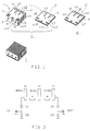
- Fig. 1 presents a three-pole filter. It comprises two parts, a dielectrical block 1 and an insulation sheet 2, Fig. 1A.
- the block is substantially rectangular, comprising a top surface and an bottom surface, two end surfaces, and two side surfaces.
- the block is provided with three holes 3,4 and 5 extending from the top surface to the bottom surface and coated with a conductive material, the openings whereof on the top surface are shown in the figure.
- the end surfaces of the block, one side surface and the bottom surface are also coated with a conductive material.
- the coated surfaces are shown in lines.
- the other side surface of the body, shown in Fig. 1A in its entirety, is not coated.
- each of the holes is joined with the coating of the undersurface of the body, whereas the coating of the top end of the hole is insulated from the coating of the sides of the block.
- a transmission line resonator is produced, the length whereof being selected according to the desired response curve of the filter.
- resonator RES1 is produced, for hole 4, resonator RES2; respectively, for hole 3, resonator RES3, Fig. 2.
- the substantially uncoated side surface of the block is provided with circuit patterns produced by metal-foil patterns for couplings to the transmission line resonators and for couplings between the resonators.
- the significance of said coupling patterns is described here, reference being made to Fig. 2, which presents the response connection of the filter of Fig. 1C.
- the pads 7 and 8 have been isolated from the coating of the side surfaces by means of insulation space 113. When a signal is carried to pad 8, it is capacitively coupled to resonator RES1. Respectively, a filtered signal is achieved from pad 7, which is coupled to the last resonator RES3, also by capacitive coupling.
- a capacitance C2 exists, Fig. 2.
- the side surface is provided with a pad 114 at the top end of resonator RES2, and at the lower end of each of the resonators, pads 9, 10 and 11.
- strips 12, resp. 13 are moreover provided, one end thereof being in connection with the coating of the bottom.
- the surface area and shape of the insulation sheet shown in Fig. 1A correspond to the surface area and shape of the side surface of the body.
- the other side surface of the sheet as well as the edges are coated all over with a conductive material.
- circuit patterns On the other side surface, visible in its entirety in the figure, circuit patterns have been arranged.
- the coating as well as the metallic circuit patterns are presented by lines. Pads 16 and 17 are isolated from the coating whereas pad 115 and strips 14 and 15 are at one end in connection with the coating.
- an insulation sheet is placed against the ceramic block with the circuit pattern surfaces so against each other that the pads 17 and 7 are placed against each other, similarly as pads 16 and 8 are placed against each other.
- a signal is carried between the pads 8 and 16 e.g. on a strip conductor (not shown).
- coupling to the filter is performed via the pad 8 of the capacitor and the capacitor C1 provided by the coating of hole 5 of resonator RES1 (Fig. 2).
- from said pad grounding is performed via pad 16 and the capacitor C3 provided by the coating of the insulation sheet 2 (Fig. 2).
- capacitors C2 and C3 are formed, where between the filtered signal is conducted out with the aid of a strip line (not shown).
- Pad 114 on the side surface of the block is grounded via pad 115 of the insulation sheet, whereby pad 114, while forming a second capacitor electrode, charges capacitively the resonator RES2, so that the resonant frequency thereof is lower than without a charge.
- the strips 12 and 15, and 13 and 14 against each other are located between two resonators, affecting the inductive coupling between said resonators.
- the pads 9,10 and 11 are not connected anywhere so that they exert no effect on the filter. Increasing the size of the pads 7 and 8 on the block increases the capacitance, thus widening the bandwidth of the filter, whereas increasing the size of the pads 16 and 17 on the insulation sheet diminishes the band-width.
- a filter such as the one shown in Fig. 1C is obtained.
- said coupling patterns it is a three-circuit bandpass filter. It is to be noted that the shape or amount of the coupling patterns bear as such no significance as regards the present invention.
- a insulation sheet of Fig. 1B may be also attached, instead of the insulation sheet as in Fig. 1A.
- the difference between the sheets lies in that the latter one is moreover provided with metal strips 18,19 and 20 connected to the coating of the edge.
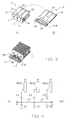
- Fig. 3 presents a three-pole stop band filter in which the coupling patterns are used as taught by the invention, both on the side surface of the block and on the surface of the insulation sheet.
- Fig. 4 presents a response circuit of the filter. Merely by the aid of said circuit patterns and two discrete components said filter can be constructed although the dimensions of the block and the insulation sheet are the same as in a three-pole band pass filter.
- pads 31,32 and 33 are located at the top end of the resonators, from which the coupling to each resonator takes place. Between the resonators strips 34 and 35 travel on the length of the entire side, one end whereof being connected to the coating of the bottom surface.
- Fig. 3 presents a three-pole stop band filter in which the coupling patterns are used as taught by the invention, both on the side surface of the block and on the surface of the insulation sheet.
- Fig. 4 presents a response circuit of the filter. Merely by the aid of said circuit patterns and two discrete components said filter can be constructed although the dimensions of the
- a coupling pattern is located, comprising pads 38,39 and 310, and two strips 36 and 37 extend from one end of the surface to the other, both ends whereof being joined to the coating of the sheet edge.
- the insulation sheet acts at the same time as a coupling sheet for coils L1 and L2 (Fig. 3C), which are soldered to pads 38,39 and 310 in the manner shown in the figure.
- the insulation sheet is attached e.g. by soldering to the block with the coupling pattern surfaces against each other so that the finger-like projections of the pads 38,39 and 310 on the insulation sheet enter on top of the equivalent pads 31,32 and 33 of the body.
- the longitudinal strips 36 and 37 are placed on top of the equivalent strips 32 and 35 of the body.
- the complete filter is shown in Fig.
- Fig. 4 presents the equivalent circuit of a filter.
- the longitudinal strip pairs 34,37 and 35,36 provide a complete isolation of the resonators from one another via the ceramic block by cancelling the electrical and magnetic field at the strip, whereby the signal moves from the resonator RES1 to resonator RES2 only via coil L1, and from resonator RES2 to resonator RES3 only via coil L2.
- the capacitances C4,C5 and C6 are formed from the capacitor formed by the pads 38,39 and 310 and the coating of one side of the insulation sheet.
- the capacitances C1, C2 and C3 are composed of a capacitor formed by pads 33,32 and 31 and holes 5,4 and 3. So, coupling to the resonators is performed capacitively.
- the embodiment shown in Fig. 4 is highly advantageous because various discrete components can be placed with ease on the flange projecting from the block 1 of the insulation sheet 2, depending on the filter. Therefore, it is obvious to a person skilled in the art to prepare e.g. a duplex filter using a single ceramic body.
- the filters of the Rx and Tx branch are separated in equivalent manner using a corresponding strip ex-tending over the surface wherewith the individual resonators in the design shown in Fig. 3 were separated.
- the discrete components required can be positioned on the flange. It is obvious to a person skilled in the art that, if desired, said flange part can be covered with a separate metal cover.
- the insulation sheet may also be part of the circuit board, whereto the radio frequency parts of the radio apparatus have been attached. It may also be smaller in the surface area than the surface area of the side surface of the body.
Landscapes
- Physics & Mathematics (AREA)
- Electromagnetism (AREA)
- Control Of Motors That Do Not Use Commutators (AREA)
Description
- The present invention relates to radio frequency filters of the type comprising a block of dielectric matter and an insulation sheet. The surfaces of the block comprise a top surface and bottom surface on the opposite sides, two opposite side surfaces limited to said surfaces, and the opposite two end surfaces. From the top surface of the block to the bottom surface at least two holes extend, coated with a conductive material. At least the main part of the surface of the body, with the exception of one side surface, has been coated with a conductive layer, whereby a transmission line resonator is produced for each hole. The insulation sheet has been attached against the uncoated side surface, the surface of which not facing the block is coated with a conductive layer.
- Known in the art are such dielectric, usually ceramic filters which have been coated all over, with the exception of the top surface, with an electrically conductive material. When the coating of a coated hole is connected with the coating of the bottom surface, the hole has been short circuited at that point. Since the top surface, at least in the vicinity of the hole, is uncoated, the hole is open at this end. The structure forms now a quarter-wave transmission line resonator. When conducting an electromagnetic wave into the structure, at a given frequency, i.e. at the resonant frequency, a standing wave in the direction of the hole is produced. The maximum of the capacitive field thereof is placed at the open end of the hole, whereas the maximum of the inductive field is placed at the short circuited hole. If on the uncoated top surface various conductive patterns are placed, both the resonant frequency of an individual resonator and the coupling between the resonators can be affected. By positioning a conductive pad adjacent to the open end of the furthermost resonators of the block, and insulated from the coating of the side of the block, a signal can be carried into the resonator by being capacitively coupled with the resonator, and out therefrom likewise by capacitive coupling. Since between the coating of the open top end of the resonator and the coating of the top side edge of the ceramic block is a given capacitance value, said capacitance can be changed by adding some coating to the proximity of the top side hole,said coating being in connection with the coating of the side, or by adding some coating on the top side in connection with the coating of the hole. This is one manner in which the resonant frequency is affected. With the aid of the conductive patterns, capacitors and transmission lines may further be arranged on the top surface also between the resonators, and so, the coupling between the resonators can be affected.
- The inductive coupling between the resonators can be affected by handling the ceramic block, e.g. by boring holes therein or by removing otherwise some of the matter.
- Positioning conductive patterns on the top surface of the ceramic block is, however, very difficult because the surface area available is very small, so that even minimal defects in the accuracy in positioning the conductor patterns greatly affect the electrical properties of the filter. In addition, by placing the conductive patterns merely on the top surface, only the capacitive field can be affected, and the couplings are therefore capacitive.
- A critical improvement in said generally used method is disclosed in the patent application EP-0 401 838 of the present applicant, Turunen et al. In the filter described therein the electrical properties of the filter can be affected in a wide range in that the side surface is substantially uncoated, and the conductive patterns and the coupling wires have been placed on said side surface of the filter block. Not only is the surface area available much larger for positioning the conductive patterns than in placing them on the top surface, but also the inductive coupling between the resonators can be affected. It is true that the inductive field is largest in the short circuited lower end of the resonator. Positioning a conductive pattern on a side surface allows making the coupling between the resonators capacitive, inductive and capacitively-inductive in one and same filter block. Also the coupling to the filter can be performed inductively, capacitively and as a combination thereof. The electrical properties of the filter are not so sensitive to minor variations in positioning the conductive patterns on a block side as they are when the patterns are positioned on the top surface with a small surface area. According to the EP application, the side on which the conductive patterns are located, is finally coated with a metallic cover. Said filter construction allows considerable freedom for the filter designer, and in practice, by using merely a few standard-sized filter blocks, it is possible, by varying the bandwidth and the mean frequency of the resonators, that is, by using different conductive patterns, filters of different types can be constructed.
- In the EP application, also another embodiment is described. As taught thereby, the side surface of the block is also substantially uncoated. An insulation sheet is placed against the side surface, the surface not facing said surface of the block as well as the edges of the sheet have been coated. The coating is electrically in connection with the coating of the block. The conductive patterns have therefore been placed on the surface of said insulation sheet positioned against the uncoated side surface of the ceramic block. This is preferable particularly when the insulation sheet is part of the circuit board whereon also the rest of the components required in the circuit are placed. Such discrete components can be, e.g. coils and surface mounted resistors. Since it is difficult to obtain high inductance valves with the conductive patterns, discrete coils are needed in a variety of filters, such as band stop filters between different resonators through which a signal passes from one resonator to another. Said discrete components are placed on the part of the insulation sheet which extends across the side surface of the filter block. Carrying a signal into a filter as well as therefrom can be performed with strip conductors via said crossing part.
- The construction according to the EP application mentioned above and particularly the embodiment in which the conductive patterns and coupling parts are placed on the insulation sheet positioned against the side surface contain serious drawbacks in spite of certain advantages. The first one is the requirement concerning the straightness of the surfaces. Both the side surface of the block and the insulation sheet placed thereagainst are required to be extremely plain so that no air gaps are left therebetween when the surfaces are placed one against the other. The second one concerns the requirement set on adjusting the insulation sheet. When the patterns are located on the insulation sheet and they must be positioned precisely on a given pad against the side surface of the block, even minor divergence in positioning generate variations in the electrical properties in the finished products, which may exceed the permitted tolerances.
- EP-0-444948 A2 describes another dielectric resonator with a dielectric block.
- In accordance with the present invention there is provided a radio frequency filter as defined in
claim 1. - The present invention provides a filter which has the advantages of the structure described in the EP patent without the drawbacks. This is achieved by providing part of the conductive patterns on the uncoated side surface of the ceramic block and part on the side surface of the insulation sheet to be set against said surface. In addition, part of the patterns may be such that in the final installation they are placed one on top of the other.
- By positioning the conductive patterns and pads on the side surface of the ceramic block in positioning whereof deviations are permitted, the requirements concerning the precision of assembly may be reduced. The mean frequency of the filter can be affected so that the same basic block is used in which the pattern of the side is kept the same but the pattern of the insulation sheet to be positioned against the side varies. Hereby, filters with different electrical properties can be produced using one and the same ceramic block, through the patterns of the side whereof majority of the couplings is performed, and by varying the insulation sheet.
- The invention and the various embodiments thereof are de-scribed with the aid of the accompanying exemplary figures, in which
- Figs. 1A-C present a three-pole bandpass filter,
- Fig. 2 shows an equivalent circuit of the filter in Fig. 1,
- Figs. 3A-C present a three-pole band stop filter, and
- Fig. 4 presents the response circuit of the filter shown in Fig. 3.
-
- Fig. 1 presents a three-pole filter. It comprises two parts, a
dielectrical block 1 and aninsulation sheet 2, Fig. 1A. The block is substantially rectangular, comprising a top surface and an bottom surface, two end surfaces, and two side surfaces. The block is provided with threeholes hole 5, resonator RES1 is produced, forhole 4, resonator RES2; respectively, forhole 3, resonator RES3, Fig. 2. - The substantially uncoated side surface of the block is provided with circuit patterns produced by metal-foil patterns for couplings to the transmission line resonators and for couplings between the resonators. The significance of said coupling patterns is described here, reference being made to Fig. 2, which presents the response connection of the filter of Fig. 1C. The
pads 7 and 8 have been isolated from the coating of the side surfaces by means ofinsulation space 113. When a signal is carried to pad 8, it is capacitively coupled to resonator RES1. Respectively, a filtered signal is achieved frompad 7, which is coupled to the last resonator RES3, also by capacitive coupling. Thus, between the pad 8 and the top end coating ofhole 5 in resonator RES1 a capacitance C2 exists, Fig. 2. In addition, the side surface is provided with apad 114 at the top end of resonator RES2, and at the lower end of each of the resonators,pads - The surface area and shape of the insulation sheet shown in Fig. 1A correspond to the surface area and shape of the side surface of the body. The other side surface of the sheet as well as the edges are coated all over with a conductive material. On the other side surface, visible in its entirety in the figure, circuit patterns have been arranged. The coating as well as the metallic circuit patterns are presented by lines.
Pads pad 115 and strips 14 and 15 are at one end in connection with the coating. - When assembling a filter, an insulation sheet is placed against the ceramic block with the circuit pattern surfaces so against each other that the
pads pads 16 and 8 are placed against each other. A signal is carried between thepads 8 and 16 e.g. on a strip conductor (not shown). When viewed from said pad, coupling to the filter is performed via the pad 8 of the capacitor and the capacitor C1 provided by the coating ofhole 5 of resonator RES1 (Fig. 2). In addition, from said pad grounding is performed viapad 16 and the capacitor C3 provided by the coating of the insulation sheet 2 (Fig. 2). Respectively, when viewed from a point between thepads Pad 114 on the side surface of the block is grounded viapad 115 of the insulation sheet, wherebypad 114, while forming a second capacitor electrode, charges capacitively the resonator RES2, so that the resonant frequency thereof is lower than without a charge. Thestrips pads pads 7 and 8 on the block increases the capacitance, thus widening the bandwidth of the filter, whereas increasing the size of thepads - After placing the block and the insulation sheet against one another and fastening to each other e.g. by soldering, a filter such as the one shown in Fig. 1C is obtained. In said coupling patterns it is a three-circuit bandpass filter. It is to be noted that the shape or amount of the coupling patterns bear as such no significance as regards the present invention.
- On the block as in Fig. 1A a insulation sheet of Fig. 1B may be also attached, instead of the insulation sheet as in Fig. 1A. The difference between the sheets lies in that the latter one is moreover provided with
metal strips pads - Fig. 3 presents a three-pole stop band filter in which the coupling patterns are used as taught by the invention, both on the side surface of the block and on the surface of the insulation sheet. Fig. 4 presents a response circuit of the filter. Merely by the aid of said circuit patterns and two discrete components said filter can be constructed although the dimensions of the block and the insulation sheet are the same as in a three-pole band pass filter. On the side surface of the
block 1,pads insulation sheet 2, Fig. 3B, a coupling pattern is located, comprisingpads strips pads pads equivalent pads equivalent strips pads - Fig. 4 presents the equivalent circuit of a filter. The longitudinal strip pairs 34,37 and 35,36 provide a complete isolation of the resonators from one another via the ceramic block by cancelling the electrical and magnetic field at the strip, whereby the signal moves from the resonator RES1 to resonator RES2 only via coil L1, and from resonator RES2 to resonator RES3 only via coil L2. The capacitances C4,C5 and C6 are formed from the capacitor formed by the
pads pads holes - The embodiment shown in Fig. 4 is highly advantageous because various discrete components can be placed with ease on the flange projecting from the
block 1 of theinsulation sheet 2, depending on the filter. Therefore, it is obvious to a person skilled in the art to prepare e.g. a duplex filter using a single ceramic body. The filters of the Rx and Tx branch are separated in equivalent manner using a corresponding strip ex-tending over the surface wherewith the individual resonators in the design shown in Fig. 3 were separated. The discrete components required can be positioned on the flange. It is obvious to a person skilled in the art that, if desired, said flange part can be covered with a separate metal cover. - When the coupling patterns are placed as taught by the invention on both the side surface of the block and the flange, numerous advantages are gained. Using the same block but varying the insulation sheet to be attached thereto, the response curve of the filter can be changed with ease. Inserting the discrete components in the filter circuit is also easy when the surface area of the insulation sheet greater than the surface area of one side of the body.
- While remaining within the protective scope of the invention, the most diverse filters can be implemented. No restrictions are set for the requirements to meet concerning the shape and number of circuit patterns, or external components possibly used. The insulation sheet may also be part of the circuit board, whereto the radio frequency parts of the radio apparatus have been attached. It may also be smaller in the surface area than the surface area of the side surface of the body.
Claims (7)
- A radio frequency filter, comprisinga dielectric block (1), having a top surface and a bottom surface opposite each other, and between them a pair of opposite end surfaces and a pair of opposite side surfaces,at least two holes (3, 4, 5) extending through the dielectric block from the top surface to the bottom surface and comprising a conductive layer on their inner surface,a first electrically conductive layer substantially covering the bottom surface, the end surfaces and the first side surface and being, at the bottom surface, in electrically conductive connection with the conductive layer on the inner surfaces of the holes so that the holes constitute resonators,an insulation sheet (2) attached to the second side surface,a second electrically conductive layer substantially covering those surfaces of the insulation sheet that are not facing the dielectric block, said second electrically conductive layer being in electrically conductive connection with the first electrically conductive layer,
characterized in thatit comprises electrically conductive coupling patterns (12, 13, 14, 15) between the dielectric block and the insulation sheet, said electrically conductive coupling patterns affecting the inductive coupling between the resonators anda first part of said electrically conductive coupling patterns (12, 13) is located on the second side surface and a second part of said electrically conductive coupling patterns (14, 15) is located on the insulation sheet. - A radio frequency filter according to claim 1, characterized in that the insulating sheet extends beyond the dielectric block adjacent one of the end surfaces.
- A radio frequency filter according to claim 2, characterized in that the part of the insulating sheet extending beyond the dielectric block forms a flange-like projection, on the coupling electrodes whereon (38, 39, 310) the discrete components of the filter (L1, L2) have been attached.
- A radio frequency filter according to claim 1, characterized in that the surface area and shape of the insulating sheet and the surface area and shape of the second side surface of the dielectric block are essentially the same.
- A radio frequency filter according to any preceding claim, characterized in that the bottom surface of the dielectric block is covered by the first electrically conductive layer while the top surface is non-conductive.
- A radio frequency filter according to any preceding claim, characterized in that said first part (12, 13) and second part (14, 15) of said electrically conductive coupling patterns overlap.
- A radio frequency filter according to any preceding claim, characterized in that the first electrically conductive layer covers the dielectric block completely except for the top surface and the second side surface.
Applications Claiming Priority (2)
| Application Number | Priority Date | Filing Date | Title |
|---|---|---|---|
| FI933056A FI99216C (en) | 1993-07-02 | 1993-07-02 | Dielectric filter |
| FI933056 | 1993-07-02 |
Publications (2)
| Publication Number | Publication Date |
|---|---|
| EP0632516A1 EP0632516A1 (en) | 1995-01-04 |
| EP0632516B1 true EP0632516B1 (en) | 2000-05-03 |
Family
ID=8538267
Family Applications (1)
| Application Number | Title | Priority Date | Filing Date |
|---|---|---|---|
| EP94304786A Expired - Lifetime EP0632516B1 (en) | 1993-07-02 | 1994-06-30 | Dielectric filter |
Country Status (6)
| Country | Link |
|---|---|
| US (1) | US5506554A (en) |
| EP (1) | EP0632516B1 (en) |
| JP (1) | JPH0758512A (en) |
| DE (1) | DE69424228T2 (en) |
| DK (1) | DK0632516T3 (en) |
| FI (1) | FI99216C (en) |
Cited By (1)
| Publication number | Priority date | Publication date | Assignee | Title |
|---|---|---|---|---|
| RU2498464C2 (en) * | 2012-01-27 | 2013-11-10 | Федеральное государственное унитарное предприятие "Ростовский-на-Дону научно-исследовательский институт радиосвязи" (ФГУП "РНИИРС") | Band-rejection filter |
Families Citing this family (41)
| Publication number | Priority date | Publication date | Assignee | Title |
|---|---|---|---|---|
| JPH06132706A (en) * | 1992-09-07 | 1994-05-13 | Murata Mfg Co Ltd | Dielectric resonance parts |
| FI102430B (en) * | 1996-09-11 | 1998-11-30 | Filtronic Lk Oy | Filtering device with impedance stage resonators |
| KR100285957B1 (en) * | 1997-11-06 | 2001-07-12 | 윤종용 | Printed circuit board for adhereing rf band pass filter and design method thereof |
| JP2003298310A (en) * | 2002-03-29 | 2003-10-17 | Ngk Spark Plug Co Ltd | Dielectric filter |
| WO2006000650A1 (en) | 2004-06-28 | 2006-01-05 | Pulse Finland Oy | Antenna component |
| FI118748B (en) * | 2004-06-28 | 2008-02-29 | Pulse Finland Oy | Chip antenna |
| FI20041455L (en) * | 2004-11-11 | 2006-05-12 | Lk Products Oy | Antenna component |
| FI20055420A0 (en) * | 2005-07-25 | 2005-07-25 | Lk Products Oy | Adjustable multi-band antenna |
| FI118782B (en) | 2005-10-14 | 2008-03-14 | Pulse Finland Oy | Adjustable antenna |
| FI119577B (en) * | 2005-11-24 | 2008-12-31 | Pulse Finland Oy | The multiband antenna component |
| US8618990B2 (en) | 2011-04-13 | 2013-12-31 | Pulse Finland Oy | Wideband antenna and methods |
| US10211538B2 (en) | 2006-12-28 | 2019-02-19 | Pulse Finland Oy | Directional antenna apparatus and methods |
| FI20075269A0 (en) | 2007-04-19 | 2007-04-19 | Pulse Finland Oy | Method and arrangement for antenna matching |
| FI120427B (en) | 2007-08-30 | 2009-10-15 | Pulse Finland Oy | Adjustable multiband antenna |
| FI20096134A0 (en) | 2009-11-03 | 2009-11-03 | Pulse Finland Oy | Adjustable antenna |
| FI20096251A0 (en) | 2009-11-27 | 2009-11-27 | Pulse Finland Oy | MIMO antenna |
| US8847833B2 (en) | 2009-12-29 | 2014-09-30 | Pulse Finland Oy | Loop resonator apparatus and methods for enhanced field control |
| FI20105158A7 (en) | 2010-02-18 | 2011-08-19 | Pulse Finland Oy | ANTENNA EQUIPPED WITH SHELL RADIATOR |
| US9406998B2 (en) | 2010-04-21 | 2016-08-02 | Pulse Finland Oy | Distributed multiband antenna and methods |
| FI20115072A0 (en) | 2011-01-25 | 2011-01-25 | Pulse Finland Oy | Multi-resonance antenna, antenna module and radio unit |
| US9673507B2 (en) | 2011-02-11 | 2017-06-06 | Pulse Finland Oy | Chassis-excited antenna apparatus and methods |
| US8648752B2 (en) | 2011-02-11 | 2014-02-11 | Pulse Finland Oy | Chassis-excited antenna apparatus and methods |
| JP5360087B2 (en) * | 2011-02-14 | 2013-12-04 | 株式会社村田製作所 | Band elimination filter |
| US8866689B2 (en) | 2011-07-07 | 2014-10-21 | Pulse Finland Oy | Multi-band antenna and methods for long term evolution wireless system |
| US9450291B2 (en) | 2011-07-25 | 2016-09-20 | Pulse Finland Oy | Multiband slot loop antenna apparatus and methods |
| US9123990B2 (en) | 2011-10-07 | 2015-09-01 | Pulse Finland Oy | Multi-feed antenna apparatus and methods |
| US9531058B2 (en) | 2011-12-20 | 2016-12-27 | Pulse Finland Oy | Loosely-coupled radio antenna apparatus and methods |
| US9484619B2 (en) | 2011-12-21 | 2016-11-01 | Pulse Finland Oy | Switchable diversity antenna apparatus and methods |
| US8988296B2 (en) | 2012-04-04 | 2015-03-24 | Pulse Finland Oy | Compact polarized antenna and methods |
| US9979078B2 (en) | 2012-10-25 | 2018-05-22 | Pulse Finland Oy | Modular cell antenna apparatus and methods |
| US10069209B2 (en) | 2012-11-06 | 2018-09-04 | Pulse Finland Oy | Capacitively coupled antenna apparatus and methods |
| US10079428B2 (en) | 2013-03-11 | 2018-09-18 | Pulse Finland Oy | Coupled antenna structure and methods |
| US9647338B2 (en) | 2013-03-11 | 2017-05-09 | Pulse Finland Oy | Coupled antenna structure and methods |
| US9634383B2 (en) | 2013-06-26 | 2017-04-25 | Pulse Finland Oy | Galvanically separated non-interacting antenna sector apparatus and methods |
| US9680212B2 (en) | 2013-11-20 | 2017-06-13 | Pulse Finland Oy | Capacitive grounding methods and apparatus for mobile devices |
| US9590308B2 (en) | 2013-12-03 | 2017-03-07 | Pulse Electronics, Inc. | Reduced surface area antenna apparatus and mobile communications devices incorporating the same |
| US9350081B2 (en) | 2014-01-14 | 2016-05-24 | Pulse Finland Oy | Switchable multi-radiator high band antenna apparatus |
| US9973228B2 (en) | 2014-08-26 | 2018-05-15 | Pulse Finland Oy | Antenna apparatus with an integrated proximity sensor and methods |
| US9948002B2 (en) | 2014-08-26 | 2018-04-17 | Pulse Finland Oy | Antenna apparatus with an integrated proximity sensor and methods |
| US9722308B2 (en) | 2014-08-28 | 2017-08-01 | Pulse Finland Oy | Low passive intermodulation distributed antenna system for multiple-input multiple-output systems and methods of use |
| US9906260B2 (en) | 2015-07-30 | 2018-02-27 | Pulse Finland Oy | Sensor-based closed loop antenna swapping apparatus and methods |
Family Cites Families (11)
| Publication number | Priority date | Publication date | Assignee | Title |
|---|---|---|---|---|
| US4891612A (en) * | 1988-11-04 | 1990-01-02 | Cascade Microtech, Inc. | Overlap interfaces between coplanar transmission lines which are tolerant to transverse and longitudinal misalignment |
| JPH0611612B2 (en) * | 1989-05-31 | 1994-02-16 | 株式会社村上精機工作所 | Electromagnetic vibration device |
| US5103197A (en) * | 1989-06-09 | 1992-04-07 | Lk-Products Oy | Ceramic band-pass filter |
| CA2037262A1 (en) * | 1990-03-02 | 1991-09-03 | Hiroyuki Sogo | Dielectric resonator and a filter using same |
| US5144269A (en) * | 1990-03-20 | 1992-09-01 | Sanyo Electric Co., Ltd. | Dielectric filter having external connection formed on dielectric substrate |
| US5045824A (en) * | 1990-09-04 | 1991-09-03 | Motorola, Inc. | Dielectric filter construction |
| US5293141A (en) * | 1991-03-25 | 1994-03-08 | Sanyo Electric Co., Ltd. | Dielectric filter having external connection terminals on dielectric substrate and antenna duplexer using the same |
| US5177458A (en) * | 1991-07-31 | 1993-01-05 | Motorola, Inc. | Dielectric filter construction having notched mounting surface |
| JP2811382B2 (en) * | 1991-12-11 | 1998-10-15 | 富士電気化学株式会社 | Dielectric filter |
| JP3101460B2 (en) * | 1992-04-03 | 2000-10-23 | 三洋電機株式会社 | Dielectric filter and duplexer using the same |
| FI114834B (en) * | 1992-10-27 | 2004-12-31 | Ngk Spark Plug Co | Dielectric filter |
-
1993
- 1993-07-02 FI FI933056A patent/FI99216C/en active IP Right Grant
-
1994
- 1994-06-30 DK DK94304786T patent/DK0632516T3/en active
- 1994-06-30 EP EP94304786A patent/EP0632516B1/en not_active Expired - Lifetime
- 1994-06-30 DE DE69424228T patent/DE69424228T2/en not_active Expired - Fee Related
- 1994-07-04 JP JP6152503A patent/JPH0758512A/en active Pending
- 1994-07-05 US US08/271,889 patent/US5506554A/en not_active Expired - Lifetime
Cited By (1)
| Publication number | Priority date | Publication date | Assignee | Title |
|---|---|---|---|---|
| RU2498464C2 (en) * | 2012-01-27 | 2013-11-10 | Федеральное государственное унитарное предприятие "Ростовский-на-Дону научно-исследовательский институт радиосвязи" (ФГУП "РНИИРС") | Band-rejection filter |
Also Published As
| Publication number | Publication date |
|---|---|
| DK0632516T3 (en) | 2000-08-07 |
| FI933056A0 (en) | 1993-07-02 |
| FI99216B (en) | 1997-07-15 |
| JPH0758512A (en) | 1995-03-03 |
| FI99216C (en) | 1997-10-27 |
| EP0632516A1 (en) | 1995-01-04 |
| US5506554A (en) | 1996-04-09 |
| DE69424228T2 (en) | 2001-02-01 |
| DE69424228D1 (en) | 2000-06-08 |
| FI933056L (en) | 1995-03-30 |
Similar Documents
| Publication | Publication Date | Title |
|---|---|---|
| US5506554A (en) | Dielectric filter with inductive coupling electrodes formed on an adjacent insulating layer | |
| US5239279A (en) | Ceramic duplex filter | |
| US5140497A (en) | Composite electronic component and frequency adjustment method of the same | |
| JP2662742B2 (en) | Bandpass filter | |
| EP1354502B1 (en) | High frequency printed circuit board via | |
| US5392019A (en) | Inductance device and manufacturing process thereof | |
| US6515556B1 (en) | Coupling line with an uncoupled middle portion | |
| US5404118A (en) | Band pass filter with resonator having spiral electrodes formed of coil electrodes on plurality of dielectric layers | |
| US5898403A (en) | Antenna formed of multiple dielectric substrates including shielded LC filter | |
| KR100278344B1 (en) | LC Filter | |
| US6529102B2 (en) | LC filter circuit and laminated type LC filter | |
| US7432784B2 (en) | Noise filter and mounted structure of noise filter | |
| JPH03114301A (en) | Band filter | |
| EP1988598A2 (en) | Laminate type band pass filter and diplexer using the same | |
| GB1596514A (en) | Capacitors | |
| US6160461A (en) | Multilayer noise filter including integral damping resistor | |
| US5379012A (en) | Dielectric filter device | |
| US20010050601A1 (en) | Bandpass filter | |
| JP3126244B2 (en) | High frequency LC composite parts | |
| KR100279729B1 (en) | Stacked Chip Inductors | |
| JP2000261271A (en) | Lamination type low pass filter | |
| JPH0653704A (en) | Band pass filter | |
| JP3112554B2 (en) | Low pass filter for high frequency | |
| JP2780166B2 (en) | Stripline filter bandwidth adjustment method | |
| JP3368404B2 (en) | Resonators and filters |
Legal Events
| Date | Code | Title | Description |
|---|---|---|---|
| PUAI | Public reference made under article 153(3) epc to a published international application that has entered the european phase |
Free format text: ORIGINAL CODE: 0009012 |
|
| AK | Designated contracting states |
Kind code of ref document: A1 Designated state(s): CH DE DK FR GB LI |
|
| 17P | Request for examination filed |
Effective date: 19950704 |
|
| 17Q | First examination report despatched |
Effective date: 19970929 |
|
| GRAG | Despatch of communication of intention to grant |
Free format text: ORIGINAL CODE: EPIDOS AGRA |
|
| GRAG | Despatch of communication of intention to grant |
Free format text: ORIGINAL CODE: EPIDOS AGRA |
|
| GRAH | Despatch of communication of intention to grant a patent |
Free format text: ORIGINAL CODE: EPIDOS IGRA |
|
| GRAG | Despatch of communication of intention to grant |
Free format text: ORIGINAL CODE: EPIDOS AGRA |
|
| GRAH | Despatch of communication of intention to grant a patent |
Free format text: ORIGINAL CODE: EPIDOS IGRA |
|
| GRAG | Despatch of communication of intention to grant |
Free format text: ORIGINAL CODE: EPIDOS AGRA |
|
| GRAH | Despatch of communication of intention to grant a patent |
Free format text: ORIGINAL CODE: EPIDOS IGRA |
|
| GRAH | Despatch of communication of intention to grant a patent |
Free format text: ORIGINAL CODE: EPIDOS IGRA |
|
| GRAA | (expected) grant |
Free format text: ORIGINAL CODE: 0009210 |
|
| AK | Designated contracting states |
Kind code of ref document: B1 Designated state(s): CH DE DK FR GB LI |
|
| PG25 | Lapsed in a contracting state [announced via postgrant information from national office to epo] |
Ref country code: LI Free format text: LAPSE BECAUSE OF FAILURE TO SUBMIT A TRANSLATION OF THE DESCRIPTION OR TO PAY THE FEE WITHIN THE PRESCRIBED TIME-LIMIT Effective date: 20000503 Ref country code: CH Free format text: LAPSE BECAUSE OF FAILURE TO SUBMIT A TRANSLATION OF THE DESCRIPTION OR TO PAY THE FEE WITHIN THE PRESCRIBED TIME-LIMIT Effective date: 20000503 |
|
| REG | Reference to a national code |
Ref country code: CH Ref legal event code: EP |
|
| REF | Corresponds to: |
Ref document number: 69424228 Country of ref document: DE Date of ref document: 20000608 |
|
| REG | Reference to a national code |
Ref country code: DK Ref legal event code: T3 |
|
| ET | Fr: translation filed | ||
| RAP2 | Party data changed (patent owner data changed or rights of a patent transferred) |
Owner name: FILTRONIC LK OY |
|
| REG | Reference to a national code |
Ref country code: CH Ref legal event code: PL |
|
| REG | Reference to a national code |
Ref country code: FR Ref legal event code: CD |
|
| PLBE | No opposition filed within time limit |
Free format text: ORIGINAL CODE: 0009261 |
|
| STAA | Information on the status of an ep patent application or granted ep patent |
Free format text: STATUS: NO OPPOSITION FILED WITHIN TIME LIMIT |
|
| 26N | No opposition filed | ||
| REG | Reference to a national code |
Ref country code: GB Ref legal event code: IF02 |
|
| REG | Reference to a national code |
Ref country code: GB Ref legal event code: 732E |
|
| REG | Reference to a national code |
Ref country code: FR Ref legal event code: TP |
|
| REG | Reference to a national code |
Ref country code: FR Ref legal event code: CD |
|
| PGFP | Annual fee paid to national office [announced via postgrant information from national office to epo] |
Ref country code: DK Payment date: 20070618 Year of fee payment: 14 |
|
| PGFP | Annual fee paid to national office [announced via postgrant information from national office to epo] |
Ref country code: DE Payment date: 20070628 Year of fee payment: 14 |
|
| PGFP | Annual fee paid to national office [announced via postgrant information from national office to epo] |
Ref country code: GB Payment date: 20070627 Year of fee payment: 14 |
|
| PGFP | Annual fee paid to national office [announced via postgrant information from national office to epo] |
Ref country code: FR Payment date: 20070608 Year of fee payment: 14 |
|
| REG | Reference to a national code |
Ref country code: DK Ref legal event code: EBP |
|
| GBPC | Gb: european patent ceased through non-payment of renewal fee |
Effective date: 20080630 |
|
| REG | Reference to a national code |
Ref country code: FR Ref legal event code: ST Effective date: 20090228 |
|
| PG25 | Lapsed in a contracting state [announced via postgrant information from national office to epo] |
Ref country code: DE Free format text: LAPSE BECAUSE OF NON-PAYMENT OF DUE FEES Effective date: 20090101 |
|
| PG25 | Lapsed in a contracting state [announced via postgrant information from national office to epo] |
Ref country code: GB Free format text: LAPSE BECAUSE OF NON-PAYMENT OF DUE FEES Effective date: 20080630 |
|
| PG25 | Lapsed in a contracting state [announced via postgrant information from national office to epo] |
Ref country code: FR Free format text: LAPSE BECAUSE OF NON-PAYMENT OF DUE FEES Effective date: 20080630 |
|
| PG25 | Lapsed in a contracting state [announced via postgrant information from national office to epo] |
Ref country code: DK Free format text: LAPSE BECAUSE OF NON-PAYMENT OF DUE FEES Effective date: 20090106 |
|
| PG25 | Lapsed in a contracting state [announced via postgrant information from national office to epo] |
Ref country code: DK Free format text: LAPSE BECAUSE OF NON-PAYMENT OF DUE FEES Effective date: 20080630 |