EP0632509A2 - A linear integrated optocoupler and method for forming the same - Google Patents
A linear integrated optocoupler and method for forming the same Download PDFInfo
- Publication number
- EP0632509A2 EP0632509A2 EP94108642A EP94108642A EP0632509A2 EP 0632509 A2 EP0632509 A2 EP 0632509A2 EP 94108642 A EP94108642 A EP 94108642A EP 94108642 A EP94108642 A EP 94108642A EP 0632509 A2 EP0632509 A2 EP 0632509A2
- Authority
- EP
- European Patent Office
- Prior art keywords
- semiconductor substrate
- light emitting
- diode
- emitting diode
- light
- Prior art date
- Legal status (The legal status is an assumption and is not a legal conclusion. Google has not performed a legal analysis and makes no representation as to the accuracy of the status listed.)
- Granted
Links
- 238000000034 method Methods 0.000 title claims description 7
- 239000000758 substrate Substances 0.000 claims abstract description 97
- 239000004065 semiconductor Substances 0.000 claims abstract description 93
- 230000008878 coupling Effects 0.000 claims abstract description 19
- 238000010168 coupling process Methods 0.000 claims abstract description 19
- 238000005859 coupling reaction Methods 0.000 claims abstract description 19
- 239000000463 material Substances 0.000 claims abstract description 17
- 230000004907 flux Effects 0.000 abstract description 12
- 238000004519 manufacturing process Methods 0.000 description 9
- JBRZTFJDHDCESZ-UHFFFAOYSA-N AsGa Chemical compound [As]#[Ga] JBRZTFJDHDCESZ-UHFFFAOYSA-N 0.000 description 5
- 229910001218 Gallium arsenide Inorganic materials 0.000 description 5
- 230000010354 integration Effects 0.000 description 5
- 230000032683 aging Effects 0.000 description 3
- 230000008901 benefit Effects 0.000 description 3
- 238000002955 isolation Methods 0.000 description 3
- 230000003287 optical effect Effects 0.000 description 3
- 229920001296 polysiloxane Polymers 0.000 description 3
- XUIMIQQOPSSXEZ-UHFFFAOYSA-N Silicon Chemical compound [Si] XUIMIQQOPSSXEZ-UHFFFAOYSA-N 0.000 description 2
- 230000007423 decrease Effects 0.000 description 2
- 238000010586 diagram Methods 0.000 description 2
- 229910052751 metal Inorganic materials 0.000 description 2
- 239000002184 metal Substances 0.000 description 2
- 230000001681 protective effect Effects 0.000 description 2
- 229910052710 silicon Inorganic materials 0.000 description 2
- 239000010703 silicon Substances 0.000 description 2
- 239000004593 Epoxy Substances 0.000 description 1
- BQCADISMDOOEFD-UHFFFAOYSA-N Silver Chemical compound [Ag] BQCADISMDOOEFD-UHFFFAOYSA-N 0.000 description 1
- 229910052782 aluminium Inorganic materials 0.000 description 1
- XAGFODPZIPBFFR-UHFFFAOYSA-N aluminium Chemical compound [Al] XAGFODPZIPBFFR-UHFFFAOYSA-N 0.000 description 1
- 230000005540 biological transmission Effects 0.000 description 1
- 230000015556 catabolic process Effects 0.000 description 1
- 238000005530 etching Methods 0.000 description 1
- PCHJSUWPFVWCPO-UHFFFAOYSA-N gold Chemical compound [Au] PCHJSUWPFVWCPO-UHFFFAOYSA-N 0.000 description 1
- 229910052737 gold Inorganic materials 0.000 description 1
- 239000010931 gold Substances 0.000 description 1
- 238000012544 monitoring process Methods 0.000 description 1
- 238000004806 packaging method and process Methods 0.000 description 1
- 238000004886 process control Methods 0.000 description 1
- 238000012545 processing Methods 0.000 description 1
- QHGVXILFMXYDRS-UHFFFAOYSA-N pyraclofos Chemical compound C1=C(OP(=O)(OCC)SCCC)C=NN1C1=CC=C(Cl)C=C1 QHGVXILFMXYDRS-UHFFFAOYSA-N 0.000 description 1
- 230000004044 response Effects 0.000 description 1
- 229910052709 silver Inorganic materials 0.000 description 1
- 239000004332 silver Substances 0.000 description 1
- 230000005236 sound signal Effects 0.000 description 1
- 238000012360 testing method Methods 0.000 description 1
- 238000012546 transfer Methods 0.000 description 1
Images


Classifications
-
- H—ELECTRICITY
- H01—ELECTRIC ELEMENTS
- H01L—SEMICONDUCTOR DEVICES NOT COVERED BY CLASS H10
- H01L31/00—Semiconductor devices sensitive to infrared radiation, light, electromagnetic radiation of shorter wavelength or corpuscular radiation and specially adapted either for the conversion of the energy of such radiation into electrical energy or for the control of electrical energy by such radiation; Processes or apparatus specially adapted for the manufacture or treatment thereof or of parts thereof; Details thereof
- H01L31/12—Semiconductor devices sensitive to infrared radiation, light, electromagnetic radiation of shorter wavelength or corpuscular radiation and specially adapted either for the conversion of the energy of such radiation into electrical energy or for the control of electrical energy by such radiation; Processes or apparatus specially adapted for the manufacture or treatment thereof or of parts thereof; Details thereof structurally associated with, e.g. formed in or on a common substrate with, one or more electric light sources, e.g. electroluminescent light sources, and electrically or optically coupled thereto
- H01L31/16—Semiconductor devices sensitive to infrared radiation, light, electromagnetic radiation of shorter wavelength or corpuscular radiation and specially adapted either for the conversion of the energy of such radiation into electrical energy or for the control of electrical energy by such radiation; Processes or apparatus specially adapted for the manufacture or treatment thereof or of parts thereof; Details thereof structurally associated with, e.g. formed in or on a common substrate with, one or more electric light sources, e.g. electroluminescent light sources, and electrically or optically coupled thereto the semiconductor device sensitive to radiation being controlled by the light source or sources
- H01L31/167—Semiconductor devices sensitive to infrared radiation, light, electromagnetic radiation of shorter wavelength or corpuscular radiation and specially adapted either for the conversion of the energy of such radiation into electrical energy or for the control of electrical energy by such radiation; Processes or apparatus specially adapted for the manufacture or treatment thereof or of parts thereof; Details thereof structurally associated with, e.g. formed in or on a common substrate with, one or more electric light sources, e.g. electroluminescent light sources, and electrically or optically coupled thereto the semiconductor device sensitive to radiation being controlled by the light source or sources the light sources and the devices sensitive to radiation all being semiconductor devices characterised by at least one potential or surface barrier
- H01L31/173—Semiconductor devices sensitive to infrared radiation, light, electromagnetic radiation of shorter wavelength or corpuscular radiation and specially adapted either for the conversion of the energy of such radiation into electrical energy or for the control of electrical energy by such radiation; Processes or apparatus specially adapted for the manufacture or treatment thereof or of parts thereof; Details thereof structurally associated with, e.g. formed in or on a common substrate with, one or more electric light sources, e.g. electroluminescent light sources, and electrically or optically coupled thereto the semiconductor device sensitive to radiation being controlled by the light source or sources the light sources and the devices sensitive to radiation all being semiconductor devices characterised by at least one potential or surface barrier formed in, or on, a common substrate
-
- H—ELECTRICITY
- H01—ELECTRIC ELEMENTS
- H01L—SEMICONDUCTOR DEVICES NOT COVERED BY CLASS H10
- H01L2224/00—Indexing scheme for arrangements for connecting or disconnecting semiconductor or solid-state bodies and methods related thereto as covered by H01L24/00
- H01L2224/01—Means for bonding being attached to, or being formed on, the surface to be connected, e.g. chip-to-package, die-attach, "first-level" interconnects; Manufacturing methods related thereto
- H01L2224/42—Wire connectors; Manufacturing methods related thereto
- H01L2224/47—Structure, shape, material or disposition of the wire connectors after the connecting process
- H01L2224/48—Structure, shape, material or disposition of the wire connectors after the connecting process of an individual wire connector
- H01L2224/481—Disposition
- H01L2224/48151—Connecting between a semiconductor or solid-state body and an item not being a semiconductor or solid-state body, e.g. chip-to-substrate, chip-to-passive
- H01L2224/48221—Connecting between a semiconductor or solid-state body and an item not being a semiconductor or solid-state body, e.g. chip-to-substrate, chip-to-passive the body and the item being stacked
- H01L2224/48245—Connecting between a semiconductor or solid-state body and an item not being a semiconductor or solid-state body, e.g. chip-to-substrate, chip-to-passive the body and the item being stacked the item being metallic
- H01L2224/48247—Connecting between a semiconductor or solid-state body and an item not being a semiconductor or solid-state body, e.g. chip-to-substrate, chip-to-passive the body and the item being stacked the item being metallic connecting the wire to a bond pad of the item
-
- H—ELECTRICITY
- H01—ELECTRIC ELEMENTS
- H01L—SEMICONDUCTOR DEVICES NOT COVERED BY CLASS H10
- H01L2224/00—Indexing scheme for arrangements for connecting or disconnecting semiconductor or solid-state bodies and methods related thereto as covered by H01L24/00
- H01L2224/01—Means for bonding being attached to, or being formed on, the surface to be connected, e.g. chip-to-package, die-attach, "first-level" interconnects; Manufacturing methods related thereto
- H01L2224/42—Wire connectors; Manufacturing methods related thereto
- H01L2224/47—Structure, shape, material or disposition of the wire connectors after the connecting process
- H01L2224/48—Structure, shape, material or disposition of the wire connectors after the connecting process of an individual wire connector
- H01L2224/484—Connecting portions
- H01L2224/48463—Connecting portions the connecting portion on the bonding area of the semiconductor or solid-state body being a ball bond
- H01L2224/48465—Connecting portions the connecting portion on the bonding area of the semiconductor or solid-state body being a ball bond the other connecting portion not on the bonding area being a wedge bond, i.e. ball-to-wedge, regular stitch
-
- H—ELECTRICITY
- H01—ELECTRIC ELEMENTS
- H01L—SEMICONDUCTOR DEVICES NOT COVERED BY CLASS H10
- H01L2924/00—Indexing scheme for arrangements or methods for connecting or disconnecting semiconductor or solid-state bodies as covered by H01L24/00
- H01L2924/15—Details of package parts other than the semiconductor or other solid state devices to be connected
- H01L2924/181—Encapsulation
Definitions
- This invention relates, in general to op- tocouplers, and more particularly to an integrated circuit combining a light emitting diode and a detector diode on a common substrate for a linear optocoupler.
- Standard transistor optocoupler circuits are generally built and assembled from discrete components.
- a common linear optocoupler comprises a light emitting diode (LED), a detector diode (or servo detector diode), and a photo detector diode.
- the light emitting diode and the servo detector diode are gallium arsenide diodes.
- the photo detector diode is normally a silicon photo diode.
- Each component is a discrete device that is mounted and aligned within a complex package such that the detector diode and photo detector diode each receives light emitted from the light emitting diode. The components are placed in close proximity to one another to maximize light transmission and reception (within the constraints of the package) Silicone gel is sometimes used as a light flux coupling media between the light emitting diode and the servo and photo detector diodes.
- a fairly complex package must be designed to hold each component in a very exacting relationship to one another.
- a non-planar lead frame package having two opposed surfaces is well known in the optocoupler art.
- a light emitting diode and a servo detector diode are placed on one surface.
- a photo detector diode is placed on the other surface across from the LED. The photo detector diode is aligned to maximize light reception from the LED.
- This type of packaging is difficult to manufacture and expensive.
- the LED flux coupling factor between the LED and the detector diode depends on the placement accuracy of the detector diode with respect to the LED. This problem can be reduced by the use of light flux coupling media as described above.
- a linear optocoupler having a light emitting diode and a detector diode integrated on a common semiconductor substrate.
- the semiconductor substrate is transmissive to light emitted by the light emitting diode and forms a cathode for both the light emitting diode and the detector diode.
- An anode of the light emitting diode and an anode of the detector diode is formed on the substrate.
- the detector diode receives light transmitted through the semiconductor substrate.
- a method for coupling light emitted from a light emitting diode to a detector diode formed on a common semiconductor substrate is provided.
- a light emitting diode and detector diode is formed on the semiconductor substrate.
- Light emitted by the light emitting diode is transmissive to the semiconductor substrate.
- a portion of the light emitted by the light emitting diode is transmitted through the semiconductor substrate to be received by the detector diode.
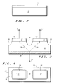
- FIG. 1 is an illustration of a common usage of a linear optocoupler 12.
- linear op- tocouplers provide non-electrical coupling between circuits.
- Some common applications for op- tocouplers are power supply feedback (volt- age/current), medical sensor isolation, audio signal interfacing, and isolation of process control transducers to name only a few.
- a light emitting diode (LED) and photo detector diode are used to create the isolation between circuits.
- the light emitting diode of a first circuit emits light that is received by the photo detector diode of a second circuit and converted to a voltage or current signal.
- the problem with using only a light emitting diode and a photo detector diode is that the LED and photodetector diode produce non-linear results.
- a linear input signal biasing the LED will produce non-linear results at the photo detector diode.
- the detector diode which is also known as a servo feedback diode, senses light transmitted by the light emitting diode and generates a current proportional to the light received from the LED. It is well known by those skilled in the art that the detector diode can be configured in either a reverse biased mode or in a photovoltaic mode to sense light emitted by the LED. A signal current/voltage generated by the detector diode is used as a control signal to servo the current driving the LED to linearize the input to output relationship. Other factors that also affect linearity are temperature, aging, and variations in light reception of the detector diode.
- the detector diode receives a constant and repeatable light flux coupling to the light emitting diode.
- Linear optocoupler 12 includes a light emitting diode 13, detector diode 18, and a photo detector diode 17.
- Light emitting diode 13 is forward biased to emit light.
- Light emitted by light emitted diode 13 is illustrated by arrows 14 and 16.
- Detector diode 18 is configured in a photovoltaic mode and photo detector diode 17 is reverse biased. The current generated by detector diode 18 and photo detector diode 17 varies with light intensity emitted by light emitting diode 13.
- An input circuit comprises an amplifier 19, a resistor 22, light emitting diode (LED) 13, and detector diode 18.
- a voltage source 21 supplies an input signal to amplifier 19.
- An output circuit, optically isolated from the input circuit comprises photo detector diode 17, resistor 24 and buffer amplifier 23.
- Detector diode 18 is in the feedback path of amplifier 19. Detector diode 18 is coupled in the photovoltaic mode in circuit 11. Coupling detector diode 18 in the photovoltaic mode generates no current when LED 13 is off. Using detector diode 18 in the photovoltaic mode requires extremely good light flux coupling with LED 13 which is difficult to achieve with discrete components. A portion of the emitted light from light emitting diode 13 is received by detector diode 18 and converted to a current/voltage which is applied to a negative input of amplifier 19. Calculating the overall gain (positive input of amplifier 19 to an output 26 of circuit 11 yields a transfer function that is independent of light emitting diode 13 bias current. The use of feedback to improve linearity is well known in the art. The ability of detector diode 18 to accurately receive light emitted by light emitting diode 13 under all operating conditions is critical to circuit 11 linearity.
- FIG. 2 is a cross-sectional view of epitaxial layer 27 formed on a semiconductor substrate 33.
- semiconductor substrate 33 is gallium arsenide.
- Gallium Arsenide has two properties which make it suitable for a linear optocoupler application. First, light emitting diodes that emit light in the infra-red range are easily formed on gallium arsenide. Second, gallium arsenide is transmissive to infrared signals. Similarly, other semiconductor materials such as silicon can equally be used as the semiconductor substrate as long as the emitted light from the light emitting diode formed on the semiconductor substrate is transmissive to the semiconductor substrate.
- Epitaxial layer 27 is formed on one planar side of semiconductor substrate 33. Epitaxial layer 27 and semiconductor substrate 33 form a diode. Epitaxial layer 27 corresponds to an anode of the diode. Semiconductor substrate 33 corresponds to a cathode of the diode.
- FIG. 3 is a cross-sectional view of a light emitting diode 28 and a detector diode 29 integrated on a semiconductor substrate 33 in accordance with the present invention.
- FIG. 3 corresponds to FIG. 2, illustrating further process steps needed to form light emitting diode 28 and detector diode 29.
- Two isolated epitaxial regions are formed on semiconductor substrate 33 by etching channels 39 through epitaxial layer 27 (of FIG. 2) to semiconductor substrate 33.
- An epitaxial region 31 forms an anode of light emitting diode 28.
- An epitaxial region 32 forms an anode of detector diode 29.
- Semiconductor substrate 33 forms a cathode for both light emitting diode 28 and detector diode 29.
- a terminal 36 couples to epitaxial region 31 and a terminal 37 couples to epitaxial region 32 providing electrical connection points.
- a layer of light reflective material 34 is formed on a second planar side of semiconductor substrate 33 opposite from which the two isolated epitaxial regions are formed.
- light reflective material 34 is electrically conductive and is chosen from a group of materials comprising gold, silver, and aluminum to name only a few.
- Light reflective material 34 electrically couples to semiconductor substrate 33.
- a terminal 38 couples to semiconductor substrate 33 for providing an electrical connection point.
- Light emitting diode 28 is normally operated in a forward biased mode and detector diode 29 is normally operated in either a reverse biased or a photovoltaic mode.
- Light is emitted, from light emitting diode 28 when it is forward biased. A portion of the emitted light transmits through semiconductor substrate 33, as illustrated by arrow 30, to be reflected off light reflective material 34. The light (illustrated by arrow 30) transmits back through semiconductor substrate 33 as shown by arrow 35 to be received by detector diode 29.
- Detector diode 29 generates a current that is a function of the reflected light received when coupled in the reverse biased or photovoltaic modes.
- semiconductor substrate 33 has a conductivity type opposite from that of epitaxial region 31 and region 32 to form light emitting diode 28 and detector diode 29.
- the characteristics of semiconductor substrate 33 and epitaxial regions 31 and 32 determine such obvious factors as the wave length of light emitted by light emitting diode 28 or breakdown voltages, these factors are tailored for the specific linear optocoupler application.
- FIG. 4 is a top view of light emitting diode 28 and detector diode 29 corresponding to FIG. 3 and illustrating isolated epitaxial region 31 and region 32.
- etched channels 39 surround epitaxial region 31 and region 32, infact, any arrangement will suffice which electrically isolates epitaxial region 31 and region 32. Electrical contact to semiconductor substrate 33 is achieved through light reflective material 34 (not shown).
- FIG. 5 is a schematic representation of light emitting diode 28 and detector diode 29 illustrated in FIG. 3.
- Terminal 38 couples to the common cathodes of light emitting diode 28 and detector diode 29.
- Terminal 36 couples to the anode of light emitting diode 28 and terminal 37 couples to the anode of detector diode 29.
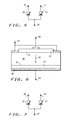
- FIG. 6 is an alternate embodiment of a light emitting diode 41 and a detector diode 42 integrated on a semiconductor substrate 40 in accordance with the present invention.
- an epitaxial layer 43 is formed on a planar side of semiconductor substrate 40.
- Epitaxial layer 43 forms an anode of light emitting diode 41.
- a terminal 48 couples to epitaxial layer 43.
- Semiconductor substrate 40 forms a cathode of light emitting diode 41.
- an epitaxial layer 44 is formed on semiconductor substrate 40.
- Epitaxial layer 44 forms an anode of detector diode 42.
- Semiconductor substrate 43 forms a cathode of detector diode 42.
- a metal layer 46 provides an electrical connection point to epitaxial layer 44.
- a terminal 49 couples to metal layer 46.
- a terminal 47 couples to semiconductor substrate 40 providing an electrical connection point..
- Light emitting diode 41 is normally operated in a forward biased mode and detector diode 42 is normally operated in a reverse biased or photovoltaic mode.
- Light is emitted from light emitting diode 41 when it is forward biased. A portion of the emitted light transmits through semiconductor substrate 40, as illustrated by arrow 45.
- Forming light emitting diode 41 and detector diode 42 on opposite sides of semiconductor substrate 40 aligns them to one another so that detector diode 42 receives light transmitted through semiconductor substrate 40 directly.
- the light received by detector diode 42 generates a current that is a function of the light received when biased in a photovoltaic or reverse biased mode. Direct reception of light by detector diode 42 provides a stable and constant light flux coupling necessary for linear op- tocouplers.
- FIG. 7 is a schematic representation of light emitting diode 41 and detector diode 42 illustrated in FIG. 6.
- Terminal 47 couples to the common cathodes of light emitting diode 41 and detector diode 42.
- Terminal 48 couples to the anode of light emitting diode 41 and terminal 49 couples to the anode of detector diode 42.
- FIG. 8 is an illustration of a photo detector diode 61 and an integrated light emitting diode 62 and detector diode 63 mounted on a lead frame 51 to form a linear optocoupler.
- Lead frame packages are well known in the art for their simple manufacture, low cost, and reliability.
- Lead frame 51 includes leads 52-57, a mounting area 58, and a mounting area 59. Mounting areas 58 and 59 are co-planar. Leads 52-57 provide electrical interconnect to photo detector diode 61, light emitting diode 62, and detector diode 63.
- Photo detector diode 61 is similar to photo detector diode 17 shown in FIG. 1. It is a discrete component that is used to isolate one circuit from another (see FIG. 1), photo detector diode 61 is optically coupled to light emitting diode 62. Photo detector diode 61 has an anode and a cathode respectively coupled to leads 54 and 53. In the preferred embodiment, attaching or mounting photo detector diode 61 to mounting area 58 also electrically couples the cathode to lead 53. A bond wire 64 couples the anode of photo detector diode 61 to lead 54. Lead 52 is unused.
- Light emitting diode 62 and detector diode 63 are formed similar to that shown in FIG. 3.
- a side not shown is metallized with a light reflective material that is electrically conductive.
- the light reflective material couples the semiconductor substrate corresponding to the common cathodes of light emitting diode 62 and detector diode 63 to lead 56.
- An anode of light emitting diode 62 is coupled to lead 55 by a bond wire 66.
- An anode of detector diode 63 is coupled to lead 57 by a bond wire 67.
- FIG. 9 is a cross-sectional view of a package 71 housing a linear optocoupler.
- FIG. 9 illustrates an optical coupling between a photo detector diode 73 and a light emitting diode 74.
- Light emitting diode 74 is integrated on a semiconductor substrate with a detector diode 75.
- a lead frame 72 has photo detector diode 73, light emitting diode 74, and detector diode 75 mounted similarly to that described in FIG. 8.
- Photo detector diode 73 and light emitting diode 74 are physically separated from one another and mounted co-planar on lead frame 72.
- Optical coupling between photo detector diode 73 and light emitting diode 74 is enhanced by a light flux coupling media 76 which channels and reflects light emitted by light emitting diode 74 to photo detector diode 73.
- light flux coupling media 76 is silicone gel.
- a protective enclosure 77 is formed around a portion of lead frame 72, light flux coupling media 76, photo detector diode 73, light emitting diode 74, and detector diode 75.
- Protective enclosure 77 is typically formed from plastic or epoxy and protects the linear optocoupler from an external environment.
- a linear optocoupler having many advantages has been described above.
- a key factor in the increased efficiency of the linear optocoupler is the integration of a light emitting diode and a detector diode on a semiconductor substrate. Integration is achieved by forming a light emitting diode that emits light at a frequency transmissive to the semiconductor substrate on which the light emitting diode is formed. Light from the light emitting diode transmits through the semiconductor substrate to be directly received by the detector diode or reflected back through the semiconductor substrate to be received by the detector diode.
- Integration of the light emitting diode and the detector diode provides many benefits to forming the linear optocoupler. Placing the detector diode in close proximity to the light emitting diode provides constant and repeatable flux coupling between the light emitting diode and the detector diode. This increases linearity that is difficult to achieve in a linear optocoupler application or increases accuracy when monitoring light output. Device sizes can also be reduced due to the close proximity of the components. Integration also reduces component count in a linear optocoupler reducing cost and manufacturing complexity.
- a linear optocoupler using discrete components has a complex and expensive package to manufacture due to the alignment of the light emitting diode to both the photo detector diode and the detector diode. Integration of the light emitting diode and the detector diode eliminates the need for external alignment between the two. Only the photo detector diode need be aligned for receiving light emitted by the light emitting diode. This alignment is made non-critical by the use of a light flux coupling media such as silicone gel described above.
- a linear optocoupler has been provided having a light emitting diode and a detector diode integrated on a common substrate that reduces size, increases accuracy, lowers cost, and decreases manufacturing complexity.
Abstract
Description
- This invention relates, in general to op- tocouplers, and more particularly to an integrated circuit combining a light emitting diode and a detector diode on a common substrate for a linear optocoupler.
- Standard transistor optocoupler circuits are generally built and assembled from discrete components. For example, a common linear optocoupler comprises a light emitting diode (LED), a detector diode (or servo detector diode), and a photo detector diode. Typically, the light emitting diode and the servo detector diode are gallium arsenide diodes. The photo detector diode is normally a silicon photo diode. Each component is a discrete device that is mounted and aligned within a complex package such that the detector diode and photo detector diode each receives light emitted from the light emitting diode. The components are placed in close proximity to one another to maximize light transmission and reception (within the constraints of the package) Silicone gel is sometimes used as a light flux coupling media between the light emitting diode and the servo and photo detector diodes.
- There are several problems that can be traced to the use of discrete components. First, a fairly complex package must be designed to hold each component in a very exacting relationship to one another. For example, a non-planar lead frame package having two opposed surfaces is well known in the optocoupler art. A light emitting diode and a servo detector diode are placed on one surface. A photo detector diode is placed on the other surface across from the LED. The photo detector diode is aligned to maximize light reception from the LED. This type of packaging is difficult to manufacture and expensive.
- Second, alignment is critical. For example, the LED flux coupling factor between the LED and the detector diode depends on the placement accuracy of the detector diode with respect to the LED. This problem can be reduced by the use of light flux coupling media as described above.
- Third, using discrete components decreases linearity of a linear optocoupler due to manufacturing tolerances. Also, temperature and aging affects are magnified due to the different manufacture of each component.
- Finally, using individual components requires more part testing, more handling, and increased potential for yield losses or field failures. It would be of great benefit if a linear optocoupler could be formed which increases linearity, simplifies manufacture, and reduces cost.
- Briefly stated, there is provided a linear optocoupler having a light emitting diode and a detector diode integrated on a common semiconductor substrate. The semiconductor substrate is transmissive to light emitted by the light emitting diode and forms a cathode for both the light emitting diode and the detector diode. An anode of the light emitting diode and an anode of the detector diode is formed on the substrate. The detector diode receives light transmitted through the semiconductor substrate.
- A method is provided for coupling light emitted from a light emitting diode to a detector diode formed on a common semiconductor substrate. A light emitting diode and detector diode is formed on the semiconductor substrate. Light emitted by the light emitting diode is transmissive to the semiconductor substrate. A portion of the light emitted by the light emitting diode is transmitted through the semiconductor substrate to be received by the detector diode.
-
- FIG. 1 is an illustration of a common usage of a linear optocoupler;
- FIG. 2 is a cross-sectional view of an epitaxial layer formed on a semiconductor substrate in accordance with the present invention;
- FIG. 3 is a cross-sectional view of an embodiment of a light emitting diode and a detector diode integrated on a semiconductor substrate in accordance with the present invention;
- FIG. 4 is a top view of the light emitting diode and the detector diode illustrated in FIG. 3 showing isolated epitaxial regions;
- FIG. 5 is a schematic diagram of the light emitting diode and the detector diode of FIG. 3 in accordance with the present invention;
- FIG. 6 is a cross-sectional view of an alternate embodiment of a light emitting diode and a detector diode integrated on a semiconductor substrate in accordance with the present invention;
- FIG. 7 is a schematic diagram of the light emitting diode and the detector diode of FIG. 6 in accordance with the present invention;
- FIG. 8 is a top view of a lead frame having a photo detector diode and an integrated light emitting diode and a detector diode mounted thereon in accordance with the present invention; and
- FIG. 9 is a cross-sectional view of a package illustrating an optical coupling between a photo detector diode and a light emitting diode in accordance with the present invention.
- FIG. 1 is an illustration of a common usage of a
linear optocoupler 12. - It is well known in the art that linear op- tocouplers provide non-electrical coupling between circuits. Some common applications for op- tocouplers are power supply feedback (volt- age/current), medical sensor isolation, audio signal interfacing, and isolation of process control transducers to name only a few. A light emitting diode (LED) and photo detector diode are used to create the isolation between circuits. The light emitting diode of a first circuit emits light that is received by the photo detector diode of a second circuit and converted to a voltage or current signal. The problem with using only a light emitting diode and a photo detector diode is that the LED and photodetector diode produce non-linear results. A linear input signal biasing the LED will produce non-linear results at the photo detector diode.
- For linear applications a detector diode is added to an optocoupler. The detector diode which is also known as a servo feedback diode, senses light transmitted by the light emitting diode and generates a current proportional to the light received from the LED. It is well known by those skilled in the art that the detector diode can be configured in either a reverse biased mode or in a photovoltaic mode to sense light emitted by the LED. A signal current/voltage generated by the detector diode is used as a control signal to servo the current driving the LED to linearize the input to output relationship. Other factors that also affect linearity are temperature, aging, and variations in light reception of the detector diode. It is essential that the detector diode receives a constant and repeatable light flux coupling to the light emitting diode. Using a discrete light emitting diode and a discrete detector diode pose multiple problems in placement, aging characteristics, and increased manufacturing costs. All of these problems can be eliminated by integrating the light emitting diode and the detector diode on a common substrate.
- A schematic of a well known optically
isolated circuit 11, using alinear optocoupler 12, and more particularly, adetector diode 18 to linearizecircuit 11 response is illustrated in FIG. 1.Linear optocoupler 12 includes alight emitting diode 13,detector diode 18, and aphoto detector diode 17.Light emitting diode 13 is forward biased to emit light. Light emitted by light emitteddiode 13 is illustrated byarrows Detector diode 18 is configured in a photovoltaic mode andphoto detector diode 17 is reverse biased. The current generated bydetector diode 18 andphoto detector diode 17 varies with light intensity emitted bylight emitting diode 13. - An input circuit comprises an
amplifier 19, aresistor 22, light emitting diode (LED) 13, anddetector diode 18. Avoltage source 21 supplies an input signal to amplifier 19. - An output circuit, optically isolated from the input circuit comprises
photo detector diode 17,resistor 24 andbuffer amplifier 23. - Linearity is achieved through the use of feedback.
Detector diode 18 is in the feedback path ofamplifier 19.Detector diode 18 is coupled in the photovoltaic mode incircuit 11.Coupling detector diode 18 in the photovoltaic mode generates no current when LED 13 is off. Usingdetector diode 18 in the photovoltaic mode requires extremely good light flux coupling withLED 13 which is difficult to achieve with discrete components. A portion of the emitted light fromlight emitting diode 13 is received bydetector diode 18 and converted to a current/voltage which is applied to a negative input ofamplifier 19. Calculating the overall gain (positive input ofamplifier 19 to anoutput 26 ofcircuit 11 yields a transfer function that is independent of light emittingdiode 13 bias current. The use of feedback to improve linearity is well known in the art. The ability ofdetector diode 18 to accurately receive light emitted by light emittingdiode 13 under all operating conditions is critical tocircuit 11 linearity. - FIG. 2 is a cross-sectional view of
epitaxial layer 27 formed on asemiconductor substrate 33. In the preferred embodiment,semiconductor substrate 33 is gallium arsenide. Gallium Arsenide has two properties which make it suitable for a linear optocoupler application. First, light emitting diodes that emit light in the infra-red range are easily formed on gallium arsenide. Second, gallium arsenide is transmissive to infrared signals. Similarly, other semiconductor materials such as silicon can equally be used as the semiconductor substrate as long as the emitted light from the light emitting diode formed on the semiconductor substrate is transmissive to the semiconductor substrate. -
Epitaxial layer 27 is formed on one planar side ofsemiconductor substrate 33.Epitaxial layer 27 andsemiconductor substrate 33 form a diode.Epitaxial layer 27 corresponds to an anode of the diode.Semiconductor substrate 33 corresponds to a cathode of the diode. - FIG. 3 is a cross-sectional view of a
light emitting diode 28 and adetector diode 29 integrated on asemiconductor substrate 33 in accordance with the present invention. FIG. 3 corresponds to FIG. 2, illustrating further process steps needed to form light emittingdiode 28 anddetector diode 29. - Two isolated epitaxial regions are formed on
semiconductor substrate 33 by etchingchannels 39 through epitaxial layer 27 (of FIG. 2) tosemiconductor substrate 33. Anepitaxial region 31 forms an anode oflight emitting diode 28. Anepitaxial region 32 forms an anode ofdetector diode 29.Semiconductor substrate 33 forms a cathode for bothlight emitting diode 28 anddetector diode 29. A terminal 36 couples toepitaxial region 31 and a terminal 37 couples toepitaxial region 32 providing electrical connection points. - A layer of light
reflective material 34 is formed on a second planar side ofsemiconductor substrate 33 opposite from which the two isolated epitaxial regions are formed. In the preferred embodiment, lightreflective material 34 is electrically conductive and is chosen from a group of materials comprising gold, silver, and aluminum to name only a few. Lightreflective material 34 electrically couples tosemiconductor substrate 33. A terminal 38 couples tosemiconductor substrate 33 for providing an electrical connection point. -
Light emitting diode 28 is normally operated in a forward biased mode anddetector diode 29 is normally operated in either a reverse biased or a photovoltaic mode. Light is emitted, from light emittingdiode 28 when it is forward biased. A portion of the emitted light transmits throughsemiconductor substrate 33, as illustrated byarrow 30, to be reflected off lightreflective material 34. The light (illustrated by arrow 30) transmits back throughsemiconductor substrate 33 as shown byarrow 35 to be received bydetector diode 29.Detector diode 29 generates a current that is a function of the reflected light received when coupled in the reverse biased or photovoltaic modes. - It is well known in the processing arts that
semiconductor substrate 33 has a conductivity type opposite from that ofepitaxial region 31 andregion 32 to form light emittingdiode 28 anddetector diode 29. The characteristics ofsemiconductor substrate 33 andepitaxial regions diode 28 or breakdown voltages, these factors are tailored for the specific linear optocoupler application. - FIG. 4 is a top view of
light emitting diode 28 anddetector diode 29 corresponding to FIG. 3 and illustratingisolated epitaxial region 31 andregion 32. In the preferred embodiment, etchedchannels 39surround epitaxial region 31 andregion 32, infact, any arrangement will suffice which electrically isolatesepitaxial region 31 andregion 32. Electrical contact tosemiconductor substrate 33 is achieved through light reflective material 34 (not shown). - FIG. 5 is a schematic representation of
light emitting diode 28 anddetector diode 29 illustrated in FIG. 3.Terminal 38 couples to the common cathodes oflight emitting diode 28 anddetector diode 29.Terminal 36 couples to the anode oflight emitting diode 28 and terminal 37 couples to the anode ofdetector diode 29. - FIG. 6 is an alternate embodiment of a
light emitting diode 41 and adetector diode 42 integrated on asemiconductor substrate 40 in accordance with the present invention. - In the embodiment of FIG. 6 an
epitaxial layer 43 is formed on a planar side ofsemiconductor substrate 40.Epitaxial layer 43 forms an anode oflight emitting diode 41. A terminal 48 couples toepitaxial layer 43.Semiconductor substrate 40 forms a cathode oflight emitting diode 41. On a planar side opposite from whichepitaxial layer 43 is formed, anepitaxial layer 44 is formed onsemiconductor substrate 40.Epitaxial layer 44 forms an anode ofdetector diode 42.Semiconductor substrate 43 forms a cathode ofdetector diode 42. Ametal layer 46 provides an electrical connection point toepitaxial layer 44. A terminal 49 couples tometal layer 46. A terminal 47 couples tosemiconductor substrate 40 providing an electrical connection point.. -
Light emitting diode 41 is normally operated in a forward biased mode anddetector diode 42 is normally operated in a reverse biased or photovoltaic mode. Light is emitted from light emittingdiode 41 when it is forward biased. A portion of the emitted light transmits throughsemiconductor substrate 40, as illustrated byarrow 45. Forminglight emitting diode 41 anddetector diode 42 on opposite sides ofsemiconductor substrate 40 aligns them to one another so thatdetector diode 42 receives light transmitted throughsemiconductor substrate 40 directly. The light received bydetector diode 42 generates a current that is a function of the light received when biased in a photovoltaic or reverse biased mode. Direct reception of light bydetector diode 42 provides a stable and constant light flux coupling necessary for linear op- tocouplers. - FIG. 7 is a schematic representation of
light emitting diode 41 anddetector diode 42 illustrated in FIG. 6.Terminal 47 couples to the common cathodes oflight emitting diode 41 anddetector diode 42.Terminal 48 couples to the anode oflight emitting diode 41 and terminal 49 couples to the anode ofdetector diode 42. - FIG. 8 is an illustration of a
photo detector diode 61 and an integratedlight emitting diode 62 anddetector diode 63 mounted on alead frame 51 to form a linear optocoupler. - Lead frame packages are well known in the art for their simple manufacture, low cost, and reliability.
Lead frame 51 includes leads 52-57, a mountingarea 58, and a mountingarea 59. Mountingareas photo detector diode 61,light emitting diode 62, anddetector diode 63. -
Photo detector diode 61 is similar tophoto detector diode 17 shown in FIG. 1. It is a discrete component that is used to isolate one circuit from another (see FIG. 1),photo detector diode 61 is optically coupled to light emittingdiode 62.Photo detector diode 61 has an anode and a cathode respectively coupled to leads 54 and 53. In the preferred embodiment, attaching or mountingphoto detector diode 61 to mountingarea 58 also electrically couples the cathode to lead 53. Abond wire 64 couples the anode ofphoto detector diode 61 to lead 54.Lead 52 is unused. -
Light emitting diode 62 anddetector diode 63 are formed similar to that shown in FIG. 3. A side not shown is metallized with a light reflective material that is electrically conductive. When attached to mountingarea 59 the light reflective material couples the semiconductor substrate corresponding to the common cathodes oflight emitting diode 62 anddetector diode 63 to lead 56. An anode oflight emitting diode 62 is coupled to lead 55 by abond wire 66. An anode ofdetector diode 63 is coupled to lead 57 by abond wire 67. This arrangement provides a simple and cost effective means for building a linear optocoupler. - FIG. 9 is a cross-sectional view of a
package 71 housing a linear optocoupler. FIG. 9 illustrates an optical coupling between aphoto detector diode 73 and a light emitting diode 74. Light emitting diode 74 is integrated on a semiconductor substrate with a detector diode 75. - A
lead frame 72 hasphoto detector diode 73, light emitting diode 74, and detector diode 75 mounted similarly to that described in FIG. 8.Photo detector diode 73 and light emitting diode 74 are physically separated from one another and mounted co-planar onlead frame 72. Optical coupling betweenphoto detector diode 73 and light emitting diode 74 is enhanced by a lightflux coupling media 76 which channels and reflects light emitted by light emitting diode 74 tophoto detector diode 73. In the preferred embodiment, lightflux coupling media 76 is silicone gel. Aprotective enclosure 77 is formed around a portion oflead frame 72, lightflux coupling media 76,photo detector diode 73, light emitting diode 74, and detector diode 75.Protective enclosure 77 is typically formed from plastic or epoxy and protects the linear optocoupler from an external environment. - A linear optocoupler having many advantages has been described above. A key factor in the increased efficiency of the linear optocoupler is the integration of a light emitting diode and a detector diode on a semiconductor substrate. Integration is achieved by forming a light emitting diode that emits light at a frequency transmissive to the semiconductor substrate on which the light emitting diode is formed. Light from the light emitting diode transmits through the semiconductor substrate to be directly received by the detector diode or reflected back through the semiconductor substrate to be received by the detector diode.
- Integration of the light emitting diode and the detector diode provides many benefits to forming the linear optocoupler. Placing the detector diode in close proximity to the light emitting diode provides constant and repeatable flux coupling between the light emitting diode and the detector diode. This increases linearity that is difficult to achieve in a linear optocoupler application or increases accuracy when monitoring light output. Device sizes can also be reduced due to the close proximity of the components. Integration also reduces component count in a linear optocoupler reducing cost and manufacturing complexity. For example, a linear optocoupler using discrete components (light emitting diode, detector diode, and photo detector diode are each a discrete component) has a complex and expensive package to manufacture due to the alignment of the light emitting diode to both the photo detector diode and the detector diode. Integration of the light emitting diode and the detector diode eliminates the need for external alignment between the two. Only the photo detector diode need be aligned for receiving light emitted by the light emitting diode. This alignment is made non-critical by the use of a light flux coupling media such as silicone gel described above. By now it should be appreciated that a linear optocoupler has been provided having a light emitting diode and a detector diode integrated on a common substrate that reduces size, increases accuracy, lowers cost, and decreases manufacturing complexity.
Claims (10)
Applications Claiming Priority (2)
| Application Number | Priority Date | Filing Date | Title |
|---|---|---|---|
| US7201693A | 1993-06-07 | 1993-06-07 | |
| US72016 | 1993-06-07 |
Publications (3)
| Publication Number | Publication Date |
|---|---|
| EP0632509A2 true EP0632509A2 (en) | 1995-01-04 |
| EP0632509A3 EP0632509A3 (en) | 1995-02-15 |
| EP0632509B1 EP0632509B1 (en) | 1997-09-24 |
Family
ID=22105038
Family Applications (1)
| Application Number | Title | Priority Date | Filing Date |
|---|---|---|---|
| EP94108642A Expired - Lifetime EP0632509B1 (en) | 1993-06-07 | 1994-06-06 | A linear integrated optocoupler and method for forming the same |
Country Status (4)
| Country | Link |
|---|---|
| US (1) | US6031251A (en) |
| EP (1) | EP0632509B1 (en) |
| JP (1) | JPH0715030A (en) |
| DE (1) | DE69405818T2 (en) |
Cited By (2)
| Publication number | Priority date | Publication date | Assignee | Title |
|---|---|---|---|---|
| WO1997002610A1 (en) * | 1995-06-30 | 1997-01-23 | Siemens Components, Inc. | Monolithic linear optocoupler |
| EP1020933A1 (en) * | 1999-01-13 | 2000-07-19 | Sharp Kabushiki Kaisha | Photocoupler device, method for fabricating the same, and lead frame for photocoupler device |
Families Citing this family (18)
| Publication number | Priority date | Publication date | Assignee | Title |
|---|---|---|---|---|
| EP1364414B1 (en) * | 2001-01-30 | 2008-12-10 | Infineon Technologies AG | A lead frame for an opto-coupler |
| ITRM20010222A1 (en) * | 2001-04-24 | 2002-10-24 | Paolo Agostinelli | SOLAR CELL POWER SUPPLY, WORKING WITH ARTIFICIAL LIGHT SOURCES, FOR ELECTRONIC EQUIPMENT. |
| US7748912B2 (en) * | 2002-10-29 | 2010-07-06 | Avago Technologies Ecbu Ip (Singapore) Pte. Ltd. | Double mold optocouplers |
| US7021839B2 (en) * | 2002-10-29 | 2006-04-04 | Dominique Ho | Low profile optocouplers |
| JP4282392B2 (en) * | 2003-07-11 | 2009-06-17 | 株式会社東芝 | Optical semiconductor device and manufacturing method thereof |
| US8395324B2 (en) * | 2009-04-20 | 2013-03-12 | Sensor Electronic Technology, Inc. | Light emitting system with dual use light element |
| JP2011181647A (en) * | 2010-03-01 | 2011-09-15 | Omron Corp | Optical coupler and producing method thereof |
| DE102010034665A1 (en) * | 2010-08-18 | 2012-02-23 | Osram Opto Semiconductors Gmbh | Optoelectronic semiconductor chip and method for producing optoelectronic semiconductor chips |
| US8587501B2 (en) * | 2011-02-17 | 2013-11-19 | Global Oled Technology Llc | Electroluminescent display device with optically communicating chiplets |
| EP2515453B1 (en) * | 2011-04-19 | 2015-08-05 | ABB Research Ltd. | Communication system for power electronic converters |
| CN102914832A (en) * | 2011-08-05 | 2013-02-06 | 快捷半导体(苏州)有限公司 | Wafer-level molded optical coupler |
| US11211305B2 (en) | 2016-04-01 | 2021-12-28 | Texas Instruments Incorporated | Apparatus and method to support thermal management of semiconductor-based components |
| US10861796B2 (en) | 2016-05-10 | 2020-12-08 | Texas Instruments Incorporated | Floating die package |
| US10179730B2 (en) | 2016-12-08 | 2019-01-15 | Texas Instruments Incorporated | Electronic sensors with sensor die in package structure cavity |
| US10074639B2 (en) | 2016-12-30 | 2018-09-11 | Texas Instruments Incorporated | Isolator integrated circuits with package structure cavity and fabrication methods |
| US10411150B2 (en) * | 2016-12-30 | 2019-09-10 | Texas Instruments Incorporated | Optical isolation systems and circuits and photon detectors with extended lateral P-N junctions |
| US9929110B1 (en) | 2016-12-30 | 2018-03-27 | Texas Instruments Incorporated | Integrated circuit wave device and method |
| US10121847B2 (en) | 2017-03-17 | 2018-11-06 | Texas Instruments Incorporated | Galvanic isolation device |
Citations (6)
| Publication number | Priority date | Publication date | Assignee | Title |
|---|---|---|---|---|
| US3229104A (en) * | 1962-12-24 | 1966-01-11 | Ibm | Four terminal electro-optical semiconductor device using light coupling |
| US3881113A (en) * | 1973-12-26 | 1975-04-29 | Ibm | Integrated optically coupled light emitter and sensor |
| US4297653A (en) * | 1979-04-30 | 1981-10-27 | Xerox Corporation | Hybrid semiconductor laser/detectors |
| EP0084621A2 (en) * | 1982-01-22 | 1983-08-03 | International Business Machines Corporation | Semiconductor signal conversion device using photon coupling |
| JPS6136981A (en) * | 1984-07-30 | 1986-02-21 | Toshiba Corp | Linear photocoupler |
| EP0318883A1 (en) * | 1987-12-02 | 1989-06-07 | Asea Brown Boveri Ab | Monolithic optocoupler |
Family Cites Families (6)
| Publication number | Priority date | Publication date | Assignee | Title |
|---|---|---|---|---|
| US3560750A (en) * | 1966-10-31 | 1971-02-02 | Hitachi Ltd | Optoelectronic amplifier |
| JPS57139976A (en) * | 1981-02-23 | 1982-08-30 | Omron Tateisi Electronics Co | Light emitting/receiving device |
| JPS5848481A (en) * | 1981-09-17 | 1983-03-22 | Nec Corp | Surface emitting type light emitting diode built in monitoring light detector |
| US4675518A (en) * | 1982-03-05 | 1987-06-23 | Omron Tateisi Electronics Co. | Optical bistable device |
| JPS59222973A (en) * | 1983-06-01 | 1984-12-14 | Nec Corp | Semiconductor optical coupling device |
| JPH0797656B2 (en) * | 1986-06-05 | 1995-10-18 | 京セラ株式会社 | Photo coupler |
-
1994
- 1994-06-01 JP JP14072194A patent/JPH0715030A/en active Pending
- 1994-06-06 DE DE69405818T patent/DE69405818T2/en not_active Expired - Fee Related
- 1994-06-06 EP EP94108642A patent/EP0632509B1/en not_active Expired - Lifetime
- 1994-11-28 US US08/345,917 patent/US6031251A/en not_active Expired - Fee Related
Patent Citations (6)
| Publication number | Priority date | Publication date | Assignee | Title |
|---|---|---|---|---|
| US3229104A (en) * | 1962-12-24 | 1966-01-11 | Ibm | Four terminal electro-optical semiconductor device using light coupling |
| US3881113A (en) * | 1973-12-26 | 1975-04-29 | Ibm | Integrated optically coupled light emitter and sensor |
| US4297653A (en) * | 1979-04-30 | 1981-10-27 | Xerox Corporation | Hybrid semiconductor laser/detectors |
| EP0084621A2 (en) * | 1982-01-22 | 1983-08-03 | International Business Machines Corporation | Semiconductor signal conversion device using photon coupling |
| JPS6136981A (en) * | 1984-07-30 | 1986-02-21 | Toshiba Corp | Linear photocoupler |
| EP0318883A1 (en) * | 1987-12-02 | 1989-06-07 | Asea Brown Boveri Ab | Monolithic optocoupler |
Non-Patent Citations (1)
| Title |
|---|
| PATENT ABSTRACTS OF JAPAN vol. 10, no. 192 (E-417) 5 July 1986 & JP-A-61 036 981 (TOSHIBA CORP) * |
Cited By (5)
| Publication number | Priority date | Publication date | Assignee | Title |
|---|---|---|---|---|
| WO1997002610A1 (en) * | 1995-06-30 | 1997-01-23 | Siemens Components, Inc. | Monolithic linear optocoupler |
| US5903016A (en) * | 1995-06-30 | 1999-05-11 | Siemens Components, Inc. | Monolithic linear optocoupler |
| CN1099137C (en) * | 1995-06-30 | 2003-01-15 | 西门子微电子公司 | Monolithic linear optocoupler |
| EP1020933A1 (en) * | 1999-01-13 | 2000-07-19 | Sharp Kabushiki Kaisha | Photocoupler device, method for fabricating the same, and lead frame for photocoupler device |
| US6507035B1 (en) | 1999-01-13 | 2003-01-14 | Sharp Kabushiki Kaisha | Photocoupler device, method for fabricating the same, and lead frame for photocoupler device |
Also Published As
| Publication number | Publication date |
|---|---|
| US6031251A (en) | 2000-02-29 |
| DE69405818T2 (en) | 1998-04-02 |
| JPH0715030A (en) | 1995-01-17 |
| EP0632509A3 (en) | 1995-02-15 |
| EP0632509B1 (en) | 1997-09-24 |
| DE69405818D1 (en) | 1997-10-30 |
Similar Documents
| Publication | Publication Date | Title |
|---|---|---|
| US6031251A (en) | Linear integrated optocoupler and method for forming the same | |
| US5753928A (en) | Monolithic optical emitter-detector | |
| US6976795B2 (en) | Optical device and optical module | |
| US4268113A (en) | Signal coupling element for substrate-mounted optical transducers | |
| US4604753A (en) | Semiconductor laser module having an improved temperature control arrangement | |
| US6987312B2 (en) | Semiconductor device with sensor and/or actuator surface and method for producing it | |
| US4124860A (en) | Optical coupler | |
| JP2002261265A (en) | Optical communication device | |
| JP2005183882A (en) | Optocoupler and electronic equipment using it | |
| JP5068443B2 (en) | Optical coupling device | |
| KR100957338B1 (en) | Passively aligned fiber optical engine for parallel optics interconnect devices | |
| JP2002076376A (en) | Optical receiving device and optical transmitting device | |
| JP2006351610A (en) | Optical module | |
| US6894314B2 (en) | Optical power monitoring for a semiconductor laser device | |
| US6606174B1 (en) | Optical semiconductor device | |
| US7067854B2 (en) | Optical receiver | |
| EP1811579A1 (en) | Galvanic optocoupler structure and corresponding hybrid integration process | |
| US11545487B2 (en) | Three-dimensional optoelectronic device package and method for manufacturing the same | |
| US7206518B2 (en) | High speed optoelectronic subassembly and package for optical devices | |
| JPH0459791B2 (en) | ||
| JPH02137275A (en) | Photo coupler | |
| CN113394208B (en) | Photoelectric detector | |
| JP3420452B2 (en) | Optical coupling device | |
| JPH05226688A (en) | Photocoupler | |
| JP2605582B2 (en) | Microwave equipment |
Legal Events
| Date | Code | Title | Description |
|---|---|---|---|
| PUAI | Public reference made under article 153(3) epc to a published international application that has entered the european phase |
Free format text: ORIGINAL CODE: 0009012 |
|
| PUAL | Search report despatched |
Free format text: ORIGINAL CODE: 0009013 |
|
| AK | Designated contracting states |
Kind code of ref document: A2 Designated state(s): DE FR GB |
|
| AK | Designated contracting states |
Kind code of ref document: A3 Designated state(s): DE FR GB |
|
| 17P | Request for examination filed |
Effective date: 19950816 |
|
| 17Q | First examination report despatched |
Effective date: 19960216 |
|
| GRAG | Despatch of communication of intention to grant |
Free format text: ORIGINAL CODE: EPIDOS AGRA |
|
| GRAH | Despatch of communication of intention to grant a patent |
Free format text: ORIGINAL CODE: EPIDOS IGRA |
|
| GRAH | Despatch of communication of intention to grant a patent |
Free format text: ORIGINAL CODE: EPIDOS IGRA |
|
| GRAA | (expected) grant |
Free format text: ORIGINAL CODE: 0009210 |
|
| AK | Designated contracting states |
Kind code of ref document: B1 Designated state(s): DE FR GB |
|
| REF | Corresponds to: |
Ref document number: 69405818 Country of ref document: DE Date of ref document: 19971030 |
|
| ET | Fr: translation filed | ||
| PLBE | No opposition filed within time limit |
Free format text: ORIGINAL CODE: 0009261 |
|
| STAA | Information on the status of an ep patent application or granted ep patent |
Free format text: STATUS: NO OPPOSITION FILED WITHIN TIME LIMIT |
|
| 26N | No opposition filed | ||
| REG | Reference to a national code |
Ref country code: GB Ref legal event code: 746 Effective date: 19990325 |
|
| PGFP | Annual fee paid to national office [announced via postgrant information from national office to epo] |
Ref country code: GB Payment date: 20000502 Year of fee payment: 7 |
|
| PG25 | Lapsed in a contracting state [announced via postgrant information from national office to epo] |
Ref country code: GB Free format text: LAPSE BECAUSE OF NON-PAYMENT OF DUE FEES Effective date: 20010606 |
|
| REG | Reference to a national code |
Ref country code: FR Ref legal event code: D6 |
|
| GBPC | Gb: european patent ceased through non-payment of renewal fee |
Effective date: 20010606 |
|
| PGFP | Annual fee paid to national office [announced via postgrant information from national office to epo] |
Ref country code: FR Payment date: 20060605 Year of fee payment: 13 |
|
| PGFP | Annual fee paid to national office [announced via postgrant information from national office to epo] |
Ref country code: DE Payment date: 20060630 Year of fee payment: 13 |
|
| REG | Reference to a national code |
Ref country code: FR Ref legal event code: ST Effective date: 20080229 |
|
| PG25 | Lapsed in a contracting state [announced via postgrant information from national office to epo] |
Ref country code: DE Free format text: LAPSE BECAUSE OF NON-PAYMENT OF DUE FEES Effective date: 20080101 |
|
| PG25 | Lapsed in a contracting state [announced via postgrant information from national office to epo] |
Ref country code: FR Free format text: LAPSE BECAUSE OF NON-PAYMENT OF DUE FEES Effective date: 20070702 |