EP0631301A1 - Method for fabrication of semiconductor power device for high commutation steepness - Google Patents
Method for fabrication of semiconductor power device for high commutation steepness Download PDFInfo
- Publication number
- EP0631301A1 EP0631301A1 EP94109103A EP94109103A EP0631301A1 EP 0631301 A1 EP0631301 A1 EP 0631301A1 EP 94109103 A EP94109103 A EP 94109103A EP 94109103 A EP94109103 A EP 94109103A EP 0631301 A1 EP0631301 A1 EP 0631301A1
- Authority
- EP
- European Patent Office
- Prior art keywords
- zone
- polished
- semiconductor body
- conductivity type
- doped
- Prior art date
- Legal status (The legal status is an assumption and is not a legal conclusion. Google has not performed a legal analysis and makes no representation as to the accuracy of the status listed.)
- Ceased
Links
- 239000004065 semiconductor Substances 0.000 title claims abstract description 28
- 238000000034 method Methods 0.000 title claims description 12
- 238000004519 manufacturing process Methods 0.000 title claims description 4
- 238000009792 diffusion process Methods 0.000 claims 2
- 230000000903 blocking effect Effects 0.000 abstract 1
- 230000001066 destructive effect Effects 0.000 abstract 1
- 230000007704 transition Effects 0.000 description 8
- 239000000463 material Substances 0.000 description 4
- 238000011161 development Methods 0.000 description 2
- 230000018109 developmental process Effects 0.000 description 2
- 238000005530 etching Methods 0.000 description 2
- 230000001939 inductive effect Effects 0.000 description 2
- ZOXJGFHDIHLPTG-UHFFFAOYSA-N Boron Chemical compound [B] ZOXJGFHDIHLPTG-UHFFFAOYSA-N 0.000 description 1
- 229910052796 boron Inorganic materials 0.000 description 1
- 239000013078 crystal Substances 0.000 description 1
- 230000006378 damage Effects 0.000 description 1
- 230000001419 dependent effect Effects 0.000 description 1
- 239000002019 doping agent Substances 0.000 description 1
- 238000005498 polishing Methods 0.000 description 1
- 238000003672 processing method Methods 0.000 description 1
- 238000000926 separation method Methods 0.000 description 1
- 239000000126 substance Substances 0.000 description 1
- 235000012431 wafers Nutrition 0.000 description 1
Images

Classifications
-
- H—ELECTRICITY
- H01—ELECTRIC ELEMENTS
- H01L—SEMICONDUCTOR DEVICES NOT COVERED BY CLASS H10
- H01L29/00—Semiconductor devices adapted for rectifying, amplifying, oscillating or switching, or capacitors or resistors with at least one potential-jump barrier or surface barrier, e.g. PN junction depletion layer or carrier concentration layer; Details of semiconductor bodies or of electrodes thereof ; Multistep manufacturing processes therefor
- H01L29/66—Types of semiconductor device ; Multistep manufacturing processes therefor
- H01L29/66007—Multistep manufacturing processes
- H01L29/66075—Multistep manufacturing processes of devices having semiconductor bodies comprising group 14 or group 13/15 materials
- H01L29/66083—Multistep manufacturing processes of devices having semiconductor bodies comprising group 14 or group 13/15 materials the devices being controllable only by variation of the electric current supplied or the electric potential applied, to one or more of the electrodes carrying the current to be rectified, amplified, oscillated or switched, e.g. two-terminal devices
- H01L29/6609—Diodes
- H01L29/66121—Multilayer diodes, e.g. PNPN diodes
-
- Y—GENERAL TAGGING OF NEW TECHNOLOGICAL DEVELOPMENTS; GENERAL TAGGING OF CROSS-SECTIONAL TECHNOLOGIES SPANNING OVER SEVERAL SECTIONS OF THE IPC; TECHNICAL SUBJECTS COVERED BY FORMER USPC CROSS-REFERENCE ART COLLECTIONS [XRACs] AND DIGESTS
- Y10—TECHNICAL SUBJECTS COVERED BY FORMER USPC
- Y10S—TECHNICAL SUBJECTS COVERED BY FORMER USPC CROSS-REFERENCE ART COLLECTIONS [XRACs] AND DIGESTS
- Y10S148/00—Metal treatment
- Y10S148/126—Power FETs
-
- Y—GENERAL TAGGING OF NEW TECHNOLOGICAL DEVELOPMENTS; GENERAL TAGGING OF CROSS-SECTIONAL TECHNOLOGIES SPANNING OVER SEVERAL SECTIONS OF THE IPC; TECHNICAL SUBJECTS COVERED BY FORMER USPC CROSS-REFERENCE ART COLLECTIONS [XRACs] AND DIGESTS
- Y10—TECHNICAL SUBJECTS COVERED BY FORMER USPC
- Y10S—TECHNICAL SUBJECTS COVERED BY FORMER USPC CROSS-REFERENCE ART COLLECTIONS [XRACs] AND DIGESTS
- Y10S438/00—Semiconductor device manufacturing: process
- Y10S438/974—Substrate surface preparation
Definitions
- the invention relates to a method for producing a power semiconductor component with at least one flat surface and with a semiconductor body with at least two zones of the first or second power type.
- Such power semiconductor devices can e.g. Diodes or thyristors.
- Diodes are not only used as uncontrolled rectifiers, but are increasingly used as free-wheeling or circuit diodes in converter circuits. In such circuits, they absorb the current imposed by an inductive load in the switch-off phase. Since this current is to be quickly commutated in the interest of a high switching speed, a high voltage arises at the inductive load, which is also present at the diode. Since a high current flows here at the same time, there are high losses in the diode, which can destroy it.
- the invention is based on the object of developing a power semiconductor component of the type mentioned in such a way that the loads mentioned can be increased without the semiconductor component being destroyed.
- This object is achieved in that a semiconductor body of the first conductivity type is polished on at least one of its flat surfaces and in that the zone of the second Line type is generated from this surface.
- the invention is based on the finding that crystal disturbances are generated in these surfaces by the usual processing methods for the surface of power semiconductor components, such as grinding or lapping. If dopants are diffused into the semiconductor body starting from such a disturbed surface, an inhomogeneous pn junction is produced. These inhomogeneities are the cause of the diode overloads and failures mentioned above. It is also conceivable that they can be used in a similar manner for the destruction of thyristors with a short dimension, e.g. asymmetrical thyristors, are responsible.
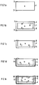
- An n-doped semiconductor body is designated by 1 in FIG. 1a. It has an upper surface 2 and a lower surface 3.
- the surface 2 is processed as usual, eg lapped and etched.
- the surface 3, however, is polished. This polishing is known from the manufacture of semiconductor wafers for integrated semiconductors. It leads to a reflective surface with an average deviation of less than 0.1 ⁇ m.
- a p-doping substance for example boron, is diffused into the semiconductor body 1 on all sides. This creates a p-doped zone 4, an n-doped zone 5 remains.
- the part of the p-doped zone 4 adjacent to the surface 2 is removed, for example by grinding, lapping or etching. This creates a surface 7.
- N-doping material is now diffused into the surface 7 after the remaining surface of the semiconductor body 1 has been provided with an oxide mask 8 (FIG. 1d).
- the edge region of the p-doped zone 4 is removed mechanically and chemically along the dashed lines 10. This creates a mesa structure. Since the heavily n-doped zone 9 was generated from the relatively strongly disturbed surface 7, the nn+ transition lying between the zones 5 and 9 is relatively inhomogeneous.
- the surface 7 can be polished like the surface 3 after grinding and etching. Then the nn+ transition between zones 5 and 9 becomes homogeneous and essentially trouble-free.
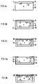
- the n-doped semiconductor body is again designated by 1.
- the upper surface 2 and the lower surface 3 are polished.
- a heavily n-doped epitaxial layer 14 is then produced on the surface 2.
- p-doping material is diffused into the semiconductor body including zone 14 on all sides. This creates a p-doped zone 16 and also zone 14 diffuses somewhat into zone 15 and p-doped layer 16.
- the part of the p-zone 16 on the side of the epitaxial layer 14 is removed. This creates a surface 17.
- the edge region of the p-doped zone 16 is removed along the dashed lines 18, so that again a mesa structure with the zone sequence n+np is created (FIG. 2c).
- the step according to FIG. 2c can be followed by two further steps instead of the separation along the dashed line 18, which are shown in FIGS. 3a and 3b.
- n-doping material can be diffused into the surface 17, so that a heavily n-doped zone 19 is formed, which adjoins the n-doped layer 14.
- the semiconductor body is provided with an oxide mask 21 on both sides and on the underside.
- the semiconductor body 1 can then be converted into a mesa structure by vertical cuts along the dashed lines 20.
- a p-doped epitaxial layer 22 (FIG. 4a) can also be produced on the polished surface 2.
- the surface 2 forms a pn junction 23 between the epitaxial zone 22 and the unchanged zone 21 of the semiconductor body 1.
- heavily n-doping material is diffused into the surface 3.
- the edge region and the top of the semiconductor body are protected by an oxide mask 24.
- the surface 3 can either be polished or lapped and etched, so that either a homogeneous, essentially undisturbed transition between zones 21 and 25 is produced or a more inhomogeneous transition.
- An inhomogeneous nn+ transition is sufficient for some applications. However, it is advantageous to create both transitions starting from a polished surface.
- diodes with a diameter of 23 mm and a reverse voltage V RM of 1700 V were commutated with a slope of 1200 A / ⁇ s. This commutation survived 90% of the diodes non-destructively.
Abstract
Description
Die Erfindung betrifft ein Verfahren zum Herstellen eines Leistungshalbleiterbauelements mit mindestens einer ebenen Oberfläche und mit einem Halbleiterkörper mit mindestens zwei Zonen vom ersten bzw. zweiten Leistungstyp.The invention relates to a method for producing a power semiconductor component with at least one flat surface and with a semiconductor body with at least two zones of the first or second power type.
Solche Leistungshalbleiterbauelement können z.B. Dioden oder auch Thyristoren sein. Dioden werden nicht nur als ungesteuerte Gleichrichter verwendet, sondern in zunehmendem Maß als Freilauf- oder Beschaltungsdioden in Stromrichterschaltungen eingesetzt. In solchen Schaltungen übernebmen sie in der Abschaltphase den von einer induktiven Last aufgezwungenen Strom. Da dieser Strom im Interesse einer hohen Schaltgeschwindigkeit schnell abkommutiert werden soll, entsteht an der induktiven Last eine hohe Spannung, die auch an der Diode anliegt. Da hier gleichzeitig ein hoher Strom fließt, kommt es zu hohen Verlusten in der Diode, wodurch diese zerstört werden kann.Such power semiconductor devices can e.g. Diodes or thyristors. Diodes are not only used as uncontrolled rectifiers, but are increasingly used as free-wheeling or circuit diodes in converter circuits. In such circuits, they absorb the current imposed by an inductive load in the switch-off phase. Since this current is to be quickly commutated in the interest of a high switching speed, a high voltage arises at the inductive load, which is also present at the diode. Since a high current flows here at the same time, there are high losses in the diode, which can destroy it.
Der Erfindung liegt die Aufgabe zugrunde, ein Leistungshalbleiterbauelement der genannten Art derart weiterzubilden, daß die genannten Belastungen erhöht werden können, ohne daß das Halbleiterbauelement zerstört wird.The invention is based on the object of developing a power semiconductor component of the type mentioned in such a way that the loads mentioned can be increased without the semiconductor component being destroyed.
Diese Aufgabe wird dadurch gelöst, daß ein Halbleiterkörper des ersten Leitungstyps mindestens auf einer seiner ebenen Oberflächen poliert wird und daß die Zone des zweiten Leitungstyps ausgehend von dieser Oberfläche erzeugt wird.This object is achieved in that a semiconductor body of the first conductivity type is polished on at least one of its flat surfaces and in that the zone of the second Line type is generated from this surface.
Weiterbildungen der Erfindung sind Gegenstand der Unteransprüche.Developments of the invention are the subject of the dependent claims.
Die Erfindung geht von der Erkenntnis aus, daß durch die üblichen Bearbeitungsverfahren der Oberfläche von Leistungshalbleiterbauelementen wie Schleifen oder Läppen in diesen Oberflächen Kristallstörungen erzeugt werden. Werden ausgehend von einer solchen gestörten Oberfläche Dotierstoffe in den Halbleiterkörper diffundiert, so entsteht ein inhomogener pn-Übergang. Diese Inhomogenitäten sind die Ursache für die oben erwähnten Überlastungen und Ausfälle der Dioden. Es ist auch denkbar, daß sie in ähnlicher Weise für die Zerstörung von hinsichtlich der Dicke knapp dimensionierten Thyristoren wie z.B. asymmetrischen Thyristoren, verantwortlich sind.The invention is based on the finding that crystal disturbances are generated in these surfaces by the usual processing methods for the surface of power semiconductor components, such as grinding or lapping. If dopants are diffused into the semiconductor body starting from such a disturbed surface, an inhomogeneous pn junction is produced. These inhomogeneities are the cause of the diode overloads and failures mentioned above. It is also conceivable that they can be used in a similar manner for the destruction of thyristors with a short dimension, e.g. asymmetrical thyristors, are responsible.
Die Erfindung wird anhand einiger Ausführungsbeispiele in Verbindung mit den Figuren 1a bis 4b näher erläutert. Dabei zeigt
- Figur 1a bis 1e
- charakteristische Verfahrensschritte eines ersten Ausführungsbeispiels
- Figur 2a bis 2c
- charakteristische Verfahrensschritte eines zweiten Ausführungsbeispiels
- Figur 3a und 3b
- eine fakultative Weiterbildung der Schritte nach Figur 2a bis 2c und
- Figur 4a und 4b
- charakteristische Verfahrensschritte gemäß einem vierten Ausführungsbeispiel.
- Figure 1a to 1e
- characteristic method steps of a first embodiment
- Figure 2a to 2c
- characteristic method steps of a second embodiment
- Figure 3a and 3b
- an optional further development of the steps according to FIGS. 2a to 2c and
- Figure 4a and 4b
- characteristic method steps according to a fourth embodiment.
In Figur 1a ist ein n-dotierter Halbleiterkörper mit 1 bezeichnet. Er hat eine obere Oberfläche 2 und eine untere Oberfläche 3. Die Oberfläche 2 wird wie üblich bearbeitet, z.B. geläppt und geätzt. Die Oberfläche 3 hingegen wird poliert. Dieses Polieren ist aus der Herstellung von Halbleiterscheiben für integrierte Halbleiter bekannt. Es führt zu einer spiegelnden Oberfläche mit einer mittleren Abweichung von weniger als 0,1µm. Als nächster Schritt (Figur 1b) wird in den Halbleiterkörper 1 allseitig eine p-dotierende Substanz, beispielsweise Bor eindiffundiert. Dabei entsteht eine p-dotierte Zone 4, eine n-dotierte Zone 5 bleibt übrig. Zwischen beiden Zonen liegt ein pn-Übergang 6, der auf der der polierten Oberfläche 3 benachbarten Seite in hohem Maße homogen und im wesentlichen störungsfrei ist. Beim nächsten Schritt (Figur 1c) wird der auf der der Oberfläche 2 benachbarte Teil der p-dotierten Zone 4 z.B. durch Schleifen, Läppen oder Ätzen entfernt. Dabei entsteht eine Oberfläche 7. In die Oberfläche 7 wird nun n-dotierendes Material eindiffundiert, nachdem die restliche Oberfläche des Halbleiterkörpers 1 mit einer Oxidmaske 8 (Figur 1d) versehen wurde. Dabei entsteht eine stark n-dotierte Zone 9 (Figur 1e), die im wesentlichen der Kontaktierung dient. Als letzter Verfahrensschritt wird der Randbereich der p-dotierten Zone 4 mechanisch und chemisch entlang der gestrichelten Linien 10 entfernt. Damit entsteht eine Mesastruktur. Da die stark n-dotierte Zone 9 von der relativ stark gestörten Oberfläche 7 aus erzeugt wurde, ist der zwischen den Zonen 5 und 9 liegende nn⁺-Übergang relativ inhomogen.An n-doped semiconductor body is designated by 1 in FIG. 1a. It has an
Alternativ kann die Oberfläche 7 nach dem Schleifen und Ätzen wie die Oberfläche 3 poliert werden. Dann wird auch der nn⁺-Übergang zwischen den Zonen 5 und 9 homogen und im wesentlichen störungsfrei.Alternatively, the surface 7 can be polished like the
Im zweiten Ausführungsbeispiel (Figur 2a bis 2c) ist der n-dotierte Halbleiterkörper wieder mit 1 bezeichnet. Hier werden die obere Oberfläche 2 und die untere Oberfläche 3 poliert. Anschließend wird auf die Oberfläche 2 eine stark n-dotierte Epitaxieschicht 14 erzeugt. Beim nächsten Schritt (Figur 2b) wird in den Halbleiterkörper einschließlich der Zone 14 allseitig p-dotierendes Material eindiffundiert. Dabei entsteht eine p-dotierte Zone 16 und auch die Zone 14 diffundiert etwas in die Zone 15 und die p-dotierte Schicht 16 hinein. Als nächstes wird der auf der Seite der Epitaxieschicht 14 liegende Teil der p-Zone 16 entfernt. Dabei entsteht eine Oberfläche 17. Danach wird der Randbereich der p-dotierten Zone 16 entlang der gestrichelten Linien 18 entfernt, so daß wiederum eine Mesastruktur mit der Zonenfolge n⁺np entsteht (Figur 2c).In the second exemplary embodiment (FIGS. 2a to 2c), the n-doped semiconductor body is again designated by 1. Here the
Fakultativ können sich an den Schritt gemäß Figur 2c anstelle der Abtrennung entlang der gestrichelten Linie 18 zwei weitere Schritte anschließen, die in Figur 3a und 3b dargestellt sind. So kann in die Oberfläche 17 n-dotierendes Material eindiffundiert werden, so daß eine stark n-dotierte Zone 19 entsteht, die sich an die n-dotierte Schicht 14 anschließt. Dazu wird der Halbleiterkörper an den beiden Seiten und an der Unterseite mit einer Oxidmaske 21 versehen. Anschließend kann der Halbleiterkörper 1 durch senkrechte Schnitte entlang der gestrichelten Linien 20 in eine Mesastruktur umgewandelt werden.Optionally, the step according to FIG. 2c can be followed by two further steps instead of the separation along the dashed
Bei den Ausführungsformen nach Figur 2 und 3 entsteht sowohl ein sehr homogener pn-Übergang als auch ein sehr homogener nn⁺-Übergang.In the embodiments according to FIGS. 2 and 3, both a very homogeneous pn transition and a very homogeneous nn⁺ transition arise.
Anstelle der n-dotierten Epitaxieschicht kann auch auf der polierten Oberfläche 2 eine p-dotierte Epitaxieschicht 22 (Figur 4a) erzeugt werden. Dabei bildet die Oberfläche 2 einen pn-Übergang 23 zwischen der Epitaxiezone 22 und der unverändert gebliebenen Zone 21 des Halbleiterkörpers 1. Anschließend wird in die Oberfläche 3 stark n-dotierendes Material eindiffundiert. Der Randbereich und die Oberseite des Halbleiterkörpers werden dabei durch eine Oxidmaske 24 geschützt. Die Oberfläche 3 kann hierbei entweder poliert oder geläppt und geätzt sein, so daß entweder ein homogener, im wesentlichen ungestörter Übergang zwischen den Zonen 21 und 25 erzeugt wird oder ein mehr inhomogener Übergang. Für manche Anwendungszwecke reicht ein imhomogener nn⁺-Übergang aus. Vorteilhaft ist es jedoch, beide Übergänge ausgehend von einer polierten Oberfläche zu erzeugen.Instead of the n-doped epitaxial layer, a p-doped epitaxial layer 22 (FIG. 4a) can also be produced on the
Ausführungsbeispiel: Dioden mit einem Durchmesser von 23mm und einer Sperrspannung VRM von 1700 V wurden mit einer Steilheit von 1200 A/µs abkommutiert. Dieses Abkommutieren überstanden 90 % der Dioden zerstörungsfrei.Exemplary embodiment: diodes with a diameter of 23 mm and a reverse voltage V RM of 1700 V were commutated with a slope of 1200 A / µs. This commutation survived 90% of the diodes non-destructively.
Claims (8)
dadurch gekennzeichnet, daß ein Halbleiterkörper (1) des ersten Leitungstyps mindestens auf einer seiner ebenen Oberflächen (2, 3) poliert wird und daß die Zone (4, 14) des zweiten Leitungstyps ausgehend von dieser Oberfläche erzeugt wird.Method for producing a power semiconductor component with a semiconductor body with at least one flat surface and with at least two zones of the first or second conductivity type,
characterized in that a semiconductor body (1) of the first conductivity type is polished on at least one of its flat surfaces (2, 3) and in that the zone (4, 14) of the second conductivity type is produced starting from this surface.
dadurch gekennzeichnet, daß die Zone (14) des zweiten Leitungstyps durch epitaktisches Aufwachsen auf der polierten Oberfläche (12) erzeugt wird.Method according to claim 1,
characterized in that the zone (14) of the second conductivity type is created by epitaxial growth on the polished surface (12).
dadurch gekennzeichnet, daß die Zone (4) des zweiten Leitungstyps durch Eindiffusion ausgehend von der polierten Oberfläche (2) erzeugt wird.Method according to claim 1,
characterized in that the zone (4) of the second conductivity type is created by diffusion starting from the polished surface (2).
dadurch gekennzeichnet, daß auch die andere Oberfläche (3) des Halbleiterkörpers poliert wird und daß ausgehend von der anderen polierten Oberfläche eine dritte Zone durch epitaktisches Aufwachsen erzeugt wird.Method according to one of claims 1 to 3,
characterized in that the other surface (3) of the semiconductor body is also polished and that, starting from the other polished surface, a third zone is produced by epitaxial growth.
dadurch gekennzeichnet, daß auch die andere Oberfläche (3) des Halbleiterkörpers poliert wird und daß ausgehend von der anderen polierten Oberfläche durch Eindiffusion eine dritte Zone erzeugt wird.Method according to one of claims 1 to 3,
characterized in that the other surface (3) of the semiconductor body is also polished and in that a third zone is created starting from the other polished surface by diffusion.
dadurch gekennzeichnet, daß die dritte Zone vom ersten Leitungstyp und höher dotiert ist als der ursprüngliche Halbleiterkörper.Method according to claim 4 or 5,
characterized in that the third zone is doped of the first conductivity type and higher than the original semiconductor body.
dadurch gekennzeichnet, daß die dritte Zone vom zweiten Leitungstyp ist.Method according to claim 4 or 5,
characterized in that the third zone is of the second conduction type.
dadurch gekennzeichnet, daß die ebene Oberfläche spieglend poliert wird mit einer mittleren Abweichung von weniger al 0,1 µm.Method according to one of claims 1 to 7,
characterized in that the flat surface is mirror-polished with an average deviation of less than 0.1 µm.
Applications Claiming Priority (2)
| Application Number | Priority Date | Filing Date | Title |
|---|---|---|---|
| DE4320560 | 1993-06-21 | ||
| DE4320560 | 1993-06-21 |
Publications (1)
| Publication Number | Publication Date |
|---|---|
| EP0631301A1 true EP0631301A1 (en) | 1994-12-28 |
Family
ID=6490849
Family Applications (1)
| Application Number | Title | Priority Date | Filing Date |
|---|---|---|---|
| EP94109103A Ceased EP0631301A1 (en) | 1993-06-21 | 1994-06-14 | Method for fabrication of semiconductor power device for high commutation steepness |
Country Status (3)
| Country | Link |
|---|---|
| US (1) | US5472908A (en) |
| EP (1) | EP0631301A1 (en) |
| JP (1) | JPH0799173A (en) |
Citations (4)
| Publication number | Priority date | Publication date | Assignee | Title |
|---|---|---|---|---|
| DE2411517A1 (en) * | 1973-03-12 | 1974-09-26 | Hitachi Ltd | METHOD FOR PRODUCING A LIGHT SENSITIVE HETEROGENIC DIODE |
| FR2317768A1 (en) * | 1975-07-10 | 1977-02-04 | Silec Semi Conducteurs | Rapid diode with rigid junction and thin I:zone, mfr. - by reinforcing wafer with polysilicon layers |
| EP0190935A2 (en) * | 1985-02-08 | 1986-08-13 | Kabushiki Kaisha Toshiba | Method of manufacturing semiconductor devices using a bonding process |
| EP0190508A2 (en) * | 1985-02-08 | 1986-08-13 | Kabushiki Kaisha Toshiba | Method of manufacturing compound semiconductor apparatus |
Family Cites Families (7)
| Publication number | Priority date | Publication date | Assignee | Title |
|---|---|---|---|---|
| BE536122A (en) * | 1954-03-05 | |||
| NL135876C (en) * | 1963-06-11 | |||
| US3954534A (en) * | 1974-10-29 | 1976-05-04 | Xerox Corporation | Method of forming light emitting diode array with dome geometry |
| EP0161740B1 (en) * | 1984-05-09 | 1991-06-12 | Kabushiki Kaisha Toshiba | Method of manufacturing semiconductor substrate |
| DE3815615A1 (en) * | 1988-05-07 | 1989-11-16 | Bosch Gmbh Robert | METHOD FOR PRODUCING A HIGH-BLOCKING PERFORMANCE DIODE |
| JPH0691263B2 (en) * | 1988-10-19 | 1994-11-14 | 株式会社東芝 | Method for manufacturing semiconductor device |
| DE4133820A1 (en) * | 1991-10-12 | 1993-04-15 | Bosch Gmbh Robert | METHOD FOR PRODUCING SEMICONDUCTOR ELEMENTS |
-
1994
- 1994-06-14 EP EP94109103A patent/EP0631301A1/en not_active Ceased
- 1994-06-15 JP JP6156536A patent/JPH0799173A/en active Pending
- 1994-06-21 US US08/263,376 patent/US5472908A/en not_active Expired - Lifetime
Patent Citations (4)
| Publication number | Priority date | Publication date | Assignee | Title |
|---|---|---|---|---|
| DE2411517A1 (en) * | 1973-03-12 | 1974-09-26 | Hitachi Ltd | METHOD FOR PRODUCING A LIGHT SENSITIVE HETEROGENIC DIODE |
| FR2317768A1 (en) * | 1975-07-10 | 1977-02-04 | Silec Semi Conducteurs | Rapid diode with rigid junction and thin I:zone, mfr. - by reinforcing wafer with polysilicon layers |
| EP0190935A2 (en) * | 1985-02-08 | 1986-08-13 | Kabushiki Kaisha Toshiba | Method of manufacturing semiconductor devices using a bonding process |
| EP0190508A2 (en) * | 1985-02-08 | 1986-08-13 | Kabushiki Kaisha Toshiba | Method of manufacturing compound semiconductor apparatus |
Non-Patent Citations (1)
| Title |
|---|
| E.V. ASTROVA ET AL., ICED '88 PROCEEDINGS OF THE INTERNATIONAL CONFERENCE ON ELECTRICAL DRIVES, vol. 1, 20 September 1988 (1988-09-20), pages A1.2.1 - A1.2.4 * |
Also Published As
| Publication number | Publication date |
|---|---|
| JPH0799173A (en) | 1995-04-11 |
| US5472908A (en) | 1995-12-05 |
Similar Documents
| Publication | Publication Date | Title |
|---|---|---|
| DE69631664T2 (en) | SiC SEMICONDUCTOR ARRANGEMENT WITH A PN TRANSITION, WHICH INCLUDES AN EDGE FOR ABSORPTION OF THE VOLTAGE | |
| DE112011103230B4 (en) | Non-punch-through bipolar power semiconductor component and a method for producing such a semiconductor component | |
| DE2845062C2 (en) | Semiconductor device and method for its manufacture | |
| DE2214935A1 (en) | Integrated semiconductor circuit | |
| DE3806164C2 (en) | ||
| DE2040911A1 (en) | Method for manufacturing a semiconductor component | |
| DE2021691A1 (en) | Semiconductor component | |
| EP0071916A2 (en) | Power MOS field effect transistor and method of producing the same | |
| DE3823795C2 (en) | ||
| EP0144876A2 (en) | Semiconductor device | |
| DE3328521C2 (en) | Rectifier diode for high reverse voltage | |
| DE2951733A1 (en) | METHOD FOR PRODUCING A SEMICONDUCTOR COMPONENT | |
| EP1003218A1 (en) | Semiconductor devices comprising a Schottky diode and a diode having a highly doped region and corresponding manufacturing methods | |
| EP0710988A2 (en) | Manufacturing method for semiconductor devices controlled by field effect | |
| DE2535864A1 (en) | SEMICONDUCTOR COMPONENTS | |
| DE3010986A1 (en) | INTEGRATED SEMICONDUCTOR CIRCUIT | |
| EP0631301A1 (en) | Method for fabrication of semiconductor power device for high commutation steepness | |
| DE3005367C2 (en) | ||
| DE19938209B4 (en) | Semiconductor device and method of manufacture | |
| EP1320897B1 (en) | Method for producing a semiconductor device consisting of semiconductor material having a reduced mean free path length and semiconductor device fabricated thereby | |
| EP0283788A1 (en) | Turn off semiconductor power device | |
| DE2316599A1 (en) | HIGH VOLTAGE SEMI-CONDUCTOR ARRANGEMENT | |
| DE1934208U (en) | SEMICONDUCTOR COMPONENT. | |
| DE2718185A1 (en) | SEMICONDUCTOR COMPOSITE ARRANGEMENT FOR HIGH VOLTAGES | |
| EP1245051B1 (en) | Dmos transistor protected against polarity reversal |
Legal Events
| Date | Code | Title | Description |
|---|---|---|---|
| PUAI | Public reference made under article 153(3) epc to a published international application that has entered the european phase |
Free format text: ORIGINAL CODE: 0009012 |
|
| AK | Designated contracting states |
Kind code of ref document: A1 Designated state(s): CH DE GB LI |
|
| 17P | Request for examination filed |
Effective date: 19950404 |
|
| 17Q | First examination report despatched |
Effective date: 19950508 |
|
| APAB | Appeal dossier modified |
Free format text: ORIGINAL CODE: EPIDOS NOAPE |
|
| APAD | Appeal reference recorded |
Free format text: ORIGINAL CODE: EPIDOS REFNE |
|
| APAD | Appeal reference recorded |
Free format text: ORIGINAL CODE: EPIDOS REFNE |
|
| STAA | Information on the status of an ep patent application or granted ep patent |
Free format text: STATUS: THE APPLICATION HAS BEEN REFUSED |
|
| 18R | Application refused |
Effective date: 20020820 |
|
| APAF | Appeal reference modified |
Free format text: ORIGINAL CODE: EPIDOSCREFNE |