EP0628832A2 - Integrated circuit with register stages - Google Patents
Integrated circuit with register stages Download PDFInfo
- Publication number
- EP0628832A2 EP0628832A2 EP94201561A EP94201561A EP0628832A2 EP 0628832 A2 EP0628832 A2 EP 0628832A2 EP 94201561 A EP94201561 A EP 94201561A EP 94201561 A EP94201561 A EP 94201561A EP 0628832 A2 EP0628832 A2 EP 0628832A2
- Authority
- EP
- European Patent Office
- Prior art keywords
- clock
- input
- signal
- output
- data
- Prior art date
- Legal status (The legal status is an assumption and is not a legal conclusion. Google has not performed a legal analysis and makes no representation as to the accuracy of the status listed.)
- Granted
Links
Images
Classifications
-
- G—PHYSICS
- G01—MEASURING; TESTING
- G01R—MEASURING ELECTRIC VARIABLES; MEASURING MAGNETIC VARIABLES
- G01R31/00—Arrangements for testing electric properties; Arrangements for locating electric faults; Arrangements for electrical testing characterised by what is being tested not provided for elsewhere
- G01R31/28—Testing of electronic circuits, e.g. by signal tracer
- G01R31/317—Testing of digital circuits
- G01R31/3181—Functional testing
- G01R31/3185—Reconfiguring for testing, e.g. LSSD, partitioning
- G01R31/318533—Reconfiguring for testing, e.g. LSSD, partitioning using scanning techniques, e.g. LSSD, Boundary Scan, JTAG
- G01R31/318541—Scan latches or cell details
-
- G—PHYSICS
- G01—MEASURING; TESTING
- G01R—MEASURING ELECTRIC VARIABLES; MEASURING MAGNETIC VARIABLES
- G01R31/00—Arrangements for testing electric properties; Arrangements for locating electric faults; Arrangements for electrical testing characterised by what is being tested not provided for elsewhere
- G01R31/28—Testing of electronic circuits, e.g. by signal tracer
- G01R31/317—Testing of digital circuits
- G01R31/3181—Functional testing
- G01R31/3185—Reconfiguring for testing, e.g. LSSD, partitioning
- G01R31/318533—Reconfiguring for testing, e.g. LSSD, partitioning using scanning techniques, e.g. LSSD, Boundary Scan, JTAG
- G01R31/318577—AC testing, e.g. current testing, burn-in
- G01R31/31858—Delay testing
Definitions
- the invention relates to an integrated circuit with a plurality of clock-controlled register stages, each of which has at least one clock input, a data input and an output and in which a flank from the clock input pulses stores a signal supplied to the data input and outputs it at the output.
- Integrated circuits must be checked for their functionality after manufacture. This is not too difficult with purely combinatorial circuits, even if they are extensive, since the number of possible signal combinations is limited even with a large number of inputs. However, this no longer applies to sequential circuits, since these contain storage elements and the signals at the outputs therefore depend not only on the test pattern currently applied to the inputs, but also on previous states. As a result, the number of signal combinations in the test patterns is so large that a complete test of the integrated circuit takes so much time that it is no longer economically possible. For this reason, various test methods have been developed in the past in order to be able to test sequential logic circuits as largely or completely as possible.
- boundary scan methods which are based on the fact that all storing elements such as register stages can be set to a special test state in which these stages are all connected in series in the form of a shift register. This allows serial test patterns to be written into the register stages, which can be read out again directly to the Check the function of the register stages themselves, and on the other hand, test patterns can be written into the register stages with which the combinatorial parts of the entire integrated circuit connected to the register stages are controlled, and the signal results supplied by these combinatorial circuit parts are taken over again by register stages, so that they can then be used for example, can be output serially.
- the object of the invention is to provide an integrated circuit with clock-edge-controlled register stages of the type mentioned at the beginning, in which the individual register stages are of simple construction and work quickly and in which a simple and reliable test operation is nevertheless possible.
- each register stage contains a series circuit of a clock-edge-controlled memory stage and a clock-level-controlled memory stage, each with at least one clock input, one data input and one output, and that the data input of the first memory stage of the series circuit includes a first multiplexer with a selection input, at least two data inputs and one data output is connected upstream, the clock-edge-controlled ones being tested during the testing of the integrated circuit
- Memory stages of the register stages at the clock input receive the same first clock signal and the clock level-controlled memory stages of the register stages receive the same second clock signal, both clock signals not having overlapping pulses, and for writing and reading out test signal patterns
- the first multiplexer at the selection input receives a first selection signal in order to provide a data input for test signals to connect its data output, and in normal operation the clock input of the clock level-controlled memory stage of the register stages is constantly supplied with a first signal value which switches this memory stage transparently.
- the edge-controlled memory stage which is used for normal operation, is simply connected in series with a simple clock-level-controlled memory stage, which is simply switched transparently in normal operation by a corresponding signal at the clock input and is therefore practically no longer effective, except that this results in the total delay is slightly increased in the register level.
- a complex logic circuit is designed with CAE tools, whereby initially only edge-controlled memory stages are used, the expansion of such a design for test purposes is easily possible.
- each register stage contains two clock-level-controlled memory stages connected in series, each with at least one clock input, one data input and one output, that the data input of the first memory stage of the series circuit has a first multiplexer with a selection input, at least two Data inputs and a data output is connected upstream and that the clock input of the second memory stage has a second multiplexer is connected upstream with a selection input, at least two clock inputs and a clock output, the first memory stages of the register stages at the clock input receiving the same first clock signal and the second multiplexers of the register stages receiving the same second clock signal at a first clock input during testing of the integrated circuit, the two clock signals not overlapping Have pulses, and for writing and reading out test signal patterns, the first multiplexer at the selection input receives a first selection signal to connect a data input for test signals to its data output, and the second multiplexer at the selection input receives a second selection signal to connect the first clock input with its clock output connect, and wherein in normal operation
- two clock level-controlled memory stages are used, which are controlled in normal operation with clock signals that are inverse to one another and thus react like an edge-controlled register stage.
- the two memory stages are controlled with two separate clock signals that do not have overlapping pulses. Due to the second multiplexer in front of the clock input of the second memory stage, this has a different delay time for the clock signal than the first memory stage, but this difference is not detrimental if the circuit is carefully dimensioned and manufactured.
- each register stage has two clock-level-controlled memory stages connected in series with at least one clock input, one data input and one output each contains a third memory stage of this type, the data input of which is connected upstream of a first multiplexer with a selection input, at least two data inputs and a data output, of which a first data input is connected to the data input of the first memory stage and that a second multiplexer is provided which has a selection input, two data inputs connected to the output of the first and third memory stages and a data output connected to the data input of the second memory stage, the second memory stages being tested during the integrated circuit test the register stages at the clock input receive the same first clock signal and the third memory stages of the register stages at the clock input receive the same second clock signal, both clock signals not having overlapping pulses, and for writing and reading out test signal patterns the first and the third multiplexer at the selection input preferably receive an identical first selection signal in order to couple a data input for test signals with the data input of the third memory stage or
- each clock level-controlled memory stage contains the series connection of a fourth multiplexer, a first and a second inverter, the fourth multiplexer having two inputs, one of which has an input with the output of the second inverter and the other input is connected to a data input, has a control input which is connected to a clock input, and an output which is connected to the input of the first inverter.
- a memory stage constructed in this way also has only one low delay, for example if it is constantly switched transparent by a corresponding clock signal.
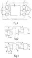
- FIG. 1 an integrated circuit 6 is shown schematically, which contains a sequential logic circuit.
- the storing elements of this circuit are indicated as register stages 1, which are connected in series as shift registers for test operation.
- a serial test pattern is fed via an input 4, which is pushed through the register stages 1 with the aid of a clock signal (not shown) and reappears at an output connection 5.
- the combinatorial parts of the logic circuit connected to the register stages are shown here in simplified form as a block 2, which is connected here to outputs or inputs of the register stages 1. For normal operation, inputs and outputs of register stages 1 are also connected to the outside via connections 3.
- test mode a test pattern is first entered via the input connection 4 and pushed through all register stages 1 until the test pattern appears completely again at the output connection 5 in order to check whether the register stages 1 all work correctly.
- a test pattern is written in such a way that all register stages 1 have a desired signal state, which of course can be different for the individual register stages, and then the output signals of the combinatorial parts 2 of the logic circuit in register stages 1 are taken over by a corresponding controller, and this The result is then pushed through the register stages 1 and removed at the output connection 5 and compared with a predetermined result.
- additional, different test patterns must then be written into the register stages 1 and the results read out again.
- Register stages 1 are often designed as clock-edge-controlled register stages, which, with a certain edge of a clock pulse, for example with the positive edge, take over a signal present at a data input when this clock edge occurs and switch it through to the output. Changes to the signal at the data input before and after this clock edge have no effect. In the system shown in Fig. 1, however, result Difficulties when the same register signal is not supplied directly to the individual register stages, but when, in particular, different clock systems are used in normal operation and these have to be interconnected in test mode via additional logic circuits.
- a register stage which feeds a combinatorial part of the logic circuit receives a result signal from this or another combinatorial circuit part and thereby changes its signal state and thus now feeds another signal into the corresponding combinatorial circuit part. If this part has an influence on the input signal of another register stage and this receives the clock signal with a delay due to logic logic elements in the clock line, this other register stage can then adopt an incorrect result.
- the register stages are therefore subject to special requirements, in particular with regard to the switchover between test operation and normal operation.
- FIG. 2 A register stage suitable for this is shown in FIG. 2.
- This consists of a clock edge-controlled memory stage 10, which can be constructed in the usual way, for example like integrated flip-flop circuits with the designation 74HC74.
- Such a memory stage has a data input that is connected to a line 13, a clock input that is connected to a clock line 16, and at least one output that is connected to a line 11. Complementary outputs are often also brought out from such memory stages.
- the clock edge-controlled memory stage 10 is preceded by a clock level-controlled memory stage 12, which also has a data input connected to a line 15 is connected, a clock input which is connected to a line 18 and has an output connected to the line 13.
- a memory stage has the property that at a value of the clock signal on line 18, for example at a high signal value, the data signal of line 15 is passed directly to output 13, this output following every change in the data signal at the data input.
- Such a storage level is therefore also referred to as a "transparent latch".
- the memory stage 12 is also preceded by a multiplexer 14 which, depending on the signal at a selection input, which is supplied via a line 26, switches the signal through at one of two data inputs 17 and 19 to the output 15.
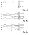
- FIG. 6a The operation of such a register stage is explained in more detail using the diagram in FIG. 6a.
- Three different sections of the operation are specified therein, the three signal profiles being designated by the numbers of the associated line in FIG. 2.
- line 26 receives a high signal as a selection signal for multiplexer 14, as a result of which data input 19 is connected to output 15. This data input 19 is connected to the output of the previous register stage or, in the first register stage of the chain, to connection 4 in FIG. 1.
- the first bit is written into memory stage 12 and there stored before the first pulse appears on the clock line 16, with the leading edge of which the data signal on line 13 is transferred to the memory stage 10 and appears at the output 11. Changes in the signal on the data line 19 or the line 15 coupled to it cannot affect between the end of the pulse on line 18 and the leading edge of the pulse on line 16, so that different delays in the clock signal on line 16 between different register stages are completely harmless. Since the two clock signals on lines 16 and 18 are supplied from outside the integrated circuit, the spacing of the pulses can be adjusted as required.
- the second section in FIG. 6a shows the processes involved in adopting a test result from a combinatorial part of the logic circuit connected to the register stage.
- the line 26 receives a low signal, as a result of which the multiplexer 14 couples the data input 17, which is connected to the output of the combinatorial subcircuit, to the line 15 and thus to the data input of the memory stage 12.
- the output signal of the combinatorial subcircuit is transferred to memory stage 12 and appears on line 13.
- the leading edge of the next pulse on line 16 which appears on line 18 a period after the end of the pulse.
- the result previously generated by the combinatorial subcircuit and temporarily stored in the memory stage 12 is transferred to the memory stage 12 and appears at the output 11. This result can be shifted to the output 5 in FIG. by on the Signal sequence in the first section in Fig. 6a is switched again.
- the signal state is shown in normal operation, so where the signal on line 18 is always high, so that the memory stage 12 is always switched to transparent, and the signal on line 26 is always low, so that the normal data input 17 is coupled to line 13 via multiplexer 14 and memory stage 12.
- the signal on the data line 17 is taken directly into the memory stage 10 and appears immediately at the output 11, i.e.
- the register stage works as desired in normal operation as a simple clock edge-controlled memory stage.
- memory stage 12 maintains the last state on data line 17, and memory stage 10 then maintains this state and no longer responds to signal changes on data line 17. This may be for one Low-power idle state can be important, since then no more signal changes occur in the register stage, so that this practically no longer consumes power.
- the register stage shown in FIG. 3 has a structure similar to that in FIG. 2. The difference essentially consists in the interchanging of the two memory stages, ie a clock level-controlled memory stage 22 is connected downstream of a clock-edge-controlled memory stage 20.
- the structure of the two memory stages and the multiplexer 24, which is the data input 25 here Storage stage 20 is connected upstream, can correspond to the structure of the corresponding stages in Fig. 2.
- the memory stage 22 is again switched permanently transparent by a high signal on the clock line 18, so that a data signal taken over by the memory stage 20 is not only on the line 21 but also after a slight delay due to the now transparently switched memory stage 22 also appears at the output 23.
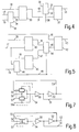
- the register stage shown in FIG. 4 contains only two clock level-controlled memory stages 30 and 32, which are connected in series with respect to the data signal.
- the data input of the first memory stage 30 is again preceded by a multiplexer 34 which, via a selection signal on line 26, couples a first data input 17 or a second data input 19 to a line 35 which leads to the data input of memory stage 30.
- a clock signal is fed to the clock input of this memory stage via line 16.
- the output of the memory stage 30 is connected via line 31 to the data input of the memory stage 32.
- the action input of the memory stage 32 is connected via a line 37 to the output of a second multiplexer 36 which, depending on a selection signal on a line 38 at the selection input, couples a clock input connected to a clock line 18 or a clock input connected to a line 39 to line 37 .
- line 38 receives a signal such that multiplexer 36 couples clock line 18 to the clock input of memory stage 32.
- line 26 receives a high signal, as shown in the first section in FIG. 6b, so that line 19 is coupled to the data input of memory stage 30.
- the memory stage 30 is switched transparent, and the data signal on the line 19 now appears on the line 31.
- the state of the memory stage 30 is recorded, and then with The memory stage 32 is switched transparent to the pulse on line 18, so that the received data signal now appears at output 33. Any changes to the data signal on line 19 can no longer have an effect once the pulse on clock line 16 ends. This enables reliable shift register operation.
- line 26 supplies a low signal to the selection input of multiplexer 34, so that data line 17 is now coupled via line 35 to the data input of memory stage 30.
- the signal on the data line 17 is transferred to the memory stage 30, while the signal state remains unchanged at the output 33 of the memory stage 32.
- Only after the end of the pulse on the clock line 16 is a pulse supplied via the clock line 18, which switches the memory stage 32 transparently, so that the signal taken over by the data line 17 now appears at the output 33.
- changes in the data signal on line 17 after the end of the pulse on clock line 16 no longer have an effect, so that no runtime problems can occur when the test results are transferred to the register stages.
- the multiplexer 36 receives a signal via the line 38 at the selection input that the clock input 39 is coupled to the line 37.
- the Clock line 39 receives the inversion of the clock pulses on clock line 16.
- a data signal is transferred to memory stage 30 with a pulse on clock line 16, while with the trailing edge of a pulse this state of memory stage 30 is recorded and at the same time memory stage 32 is switched transparently, so that the recorded state of the memory stage 30 appears at the output 33. 4 behaves like a clock edge-controlled memory stage, in which, however, the falling edges of the pulses on the clock line 16 are effective.
- this is a largely arbitrary assignment since the pulses on the clock lines 16 and 39 are inverse to one another and can also be generated, for example, by an inverter stage (not shown) within the register stage.
- the signal state on the clock line 18 in normal operation is not important in the register stage according to FIG. 4, since this clock line is then not coupled to an output line by the multiplexer.
- the multiplexer 36 is switched by a corresponding selection signal on the line 38 in such a way that the clock line 18 is coupled to the line 37 and this clock line simultaneously carries a low signal at the same time, the state of the register stage at the output 33 remains unchanged of signal changes on data lines. This is useful in order to set a temporary idle state with reduced power loss of the integrated circuit.
- both clock lines 16 and 18 have a high signal, all the memory stages 30 and 32 and thus all the register stages are switched transparently, so that in this way very much A uniform initial state of all register levels can be set quickly.
- the register stage shown in FIG. 5 uses three clock level-controlled memory stages 40, 42 and 46 and a further data multiplexer 48 between the memory stages 40 and 46 and 42, but no clock multiplexer in one of the clock lines.
- the further multiplexer 48 connects either the output of the memory stage 40 or the output of the memory stage 46 via line 45 to the data input of the memory stage 42.
- a first multiplexer 44 which is connected via the selection signal on line 49 test data to be passed on or data to be transferred from a combinatorial subcircuit is connected upstream of the data input of the memory stage 46.
- the first section again refers to the pushing through of a test pattern.
- Line 49 receives a high signal, so that the data signal of line 19 is fed to the data input of memory stage 46.
- the output of this memory stage 46 is coupled to the data input of the memory stage 42 via the multiplexer 48.
- the data signal on the data line 19 is transferred to the memory stage 46 and is then via the line 47, the multiplexer 48 and the line 45 at the data input of the memory stage 42, which is characterized by the low signal on the clock line 16 is in the memory state and therefore does not react to signals at the data input.
- the line 49 To write the test result of a combinatorial subcircuit connected to the data line 17, the line 49 first receives a low signal, as a result of which the data line 17 is coupled to the data input of the memory stage 46. It is not important that in this state the output 41 of the memory stage 40 is coupled to the data input of the memory stage 42 at the same time, since during this time the low level on the clock line 16 means that the memory stage 42 does not react to signals at the data input. With the next pulse on line 18, the data signal on line 17 is written into the memory stage 46 and permanently stored at the end of this pulse.
- Line 49 now receives a high signal again, so that the output of memory stage 46 is coupled via multiplexer 48 to the data input of memory stage 42, and then a pulse appears on clock line 16, so that memory stage 42 receives the data line 17 emits the signal received at output 43. It is therefore necessary to change the signal on line 49 between the two pulses on clock lines 18 and 16, which could only be avoided if the two multiplexers 44 and 48 were controlled with separate selection signals. However, this requires an additional line in the integrated circuit, which represents a considerable outlay.
- the line 49 constantly receives a low signal, so that the output of the memory stage is constantly on 40 is connected via line 41, multiplexer 48 and line 45 to the data input of memory stage 42.
- the memory stage 40 receives the data signal of the line 17 at the data input, and the clock input is connected to the clock line 39, which leads a signal inverse to the line 16. 5 in normal operation in a manner corresponding to the register stage in FIG. 4. Even with the register stage in FIG. 5, low-loss operation can be set when line 49 receives a high signal and clock line 18 a single one Pulse with which the data signal on line 17 is taken into memory stage 46.
- register stage described All the designs of the register stage described have in common that they can be operated both as a clock-edge-controlled register stage and as a two-phase-controlled register stage, only one additional clock line being necessary.
- the clock line used in normal operation is also used as a second phase clock in test operation and is therefore also tested at the same time.
- the register stages are only edge-controlled, so that a high processing speed is possible, while the slower two-phase operation is only effective in the test case.
- the clock level-controlled memory stages used in the register stages can be constructed in various ways.
- a particularly simple structure is shown in FIG. 7, for example. This consists of two series-connected inverter stages 50 and 52 with a conventional structure and a multiplexer 54 with two data inputs 55 and 57 and two control inputs 59 and 59a, which receive signals that are complementary to one another.
- the control signals are formed by clock signals.
- Multiplexer 54 contains two branches, each with an N-channel transistor and a P-channel transistor, which is identified by a dot on its gate. In one position of the multiplexer 54, when there is a high signal at the control input 59 and a low signal at the control input 59a, the input 55 is connected to the output, which leads to the input of the inverter 50, so that a closed ring is formed which has storage properties. Lines 51 and 53 each deliver inverse output signals from the memory stage.
- inverters 50 and 52 are also designed using complementary MOS transistor technology, a certain power loss arises in the circuit according to FIG. 7 only when switching over, but not with constant signals.
- 8 shows an embodiment of a clock level-controlled memory stage with inverters 50 and 52, the for example, are only constructed with N-channel transistors and also carry a certain current in the idle state, but here the multiplexer 54 has a simpler structure and contains only one N-channel transistor in one branch and only one P-channel transistor in the other branch . As a result, only one control input 59 is necessary.
- the input 55 of the multiplexer 54 is coupled to the inverter 50, which restores the storage state, while with a low signal at the control input 59, the input 57 of the multiplexer 54 is coupled to the inverter 50, which means that the data signal at input 57 is accepted.
Landscapes
- Engineering & Computer Science (AREA)
- General Engineering & Computer Science (AREA)
- Physics & Mathematics (AREA)
- General Physics & Mathematics (AREA)
- Power Engineering (AREA)
- Tests Of Electronic Circuits (AREA)
- Testing Or Measuring Of Semiconductors Or The Like (AREA)
Abstract
Description
Die Erfindung betrifft eine integrierte Schaltung mit mehreren taktgesteuerten Registerstufen, von denen jede wenigstens einen Takteingang, einen Dateneingang und einen Ausgang aufweist und bei der einen Flanke von dem Takteingang zugeführten Impulsen ein dem Dateneingang zugeführtes Signal speichert und am Ausgang abgibt.The invention relates to an integrated circuit with a plurality of clock-controlled register stages, each of which has at least one clock input, a data input and an output and in which a flank from the clock input pulses stores a signal supplied to the data input and outputs it at the output.
Integrierte Schaltungen müssen nach der Herstellung auf ihre Funktionsfähigkeit geprüft werden. Dies ist bei rein kombinatorisch aufgebauten Schaltungen nicht allzu schwierig, selbst wenn diese umfangreich sind, da die Anzahl der möglichen Signalkombinationen auch bei einer Vielzahl von Eingängen begrenzt ist. Dies trifft bei sequentiellen Schaltungen jedoch nicht mehr zu, da diese speichernde Elemente enthalten und somit die Signale an den Ausgängen nicht nur von dem momentan an die Eingänge angelegten Testmuster, sondern auch von vorhergehenden Zuständen abhängen. Dadurch wird die Anzahl der Signalkombinationen in den Testmustern so groß, daß ein vollständiger Test der integrierten Schaltung derart viel Zeit in Anspruch nimmt, daß er nicht mehr wirtschaftlich möglich ist. Aus diesem Grunde sind in der Vergangenheit verschiedene Testverfahren entwickelt worden, um auch sequentielle logische Schaltungen möglichst weitgehend bzw. vollständig prüfen zu können. Die bekanntesten Verfahren sind die sogenannten Boundary Scan-Verfahren, die darauf beruhen, daß alle speichernden Elemente wie Registerstufen in einen besonderen Testzustand eingestellt werden können, in dem diese Stufen alle in Form eines Schieberegisters in Reihe geschaltet sind. Dadurch können seriell Testmuster in die Registerstufen eingeschrieben werden, die direkt wieder ausgelesen werden können, um die Funktion der Registerstufen selbst zu prüfen, und andererseits können Testmuster in die Registerstufen eingeschrieben werden, mit denen die an die Registerstufen angeschlossenen kombinatorischen Teile der gesamten integrierten Schaltung angesteuert werden, und die von diesen kombinatorischen Schaltungsteilen gelieferten Signalergebnisse werden wieder von Registerstufen übernommen, damit sie danach beispielsweise seriell ausgegeben werden können.Integrated circuits must be checked for their functionality after manufacture. This is not too difficult with purely combinatorial circuits, even if they are extensive, since the number of possible signal combinations is limited even with a large number of inputs. However, this no longer applies to sequential circuits, since these contain storage elements and the signals at the outputs therefore depend not only on the test pattern currently applied to the inputs, but also on previous states. As a result, the number of signal combinations in the test patterns is so large that a complete test of the integrated circuit takes so much time that it is no longer economically possible. For this reason, various test methods have been developed in the past in order to be able to test sequential logic circuits as largely or completely as possible. The best known methods are the so-called boundary scan methods, which are based on the fact that all storing elements such as register stages can be set to a special test state in which these stages are all connected in series in the form of a shift register. This allows serial test patterns to be written into the register stages, which can be read out again directly to the Check the function of the register stages themselves, and on the other hand, test patterns can be written into the register stages with which the combinatorial parts of the entire integrated circuit connected to the register stages are controlled, and the signal results supplied by these combinatorial circuit parts are taken over again by register stages, so that they can then be used for example, can be output serially.
Derartige Verfahren sind beispielsweise in der Zeitschrift "Elektronik" Nr. 21 vom 14.10.1988, Seiten 161 bis 166 beschrieben. Darin wird u.a. auch eine Version erläutert, bei der jedem Registerelement eine sogenannte Latch-Zelle nachgeschaltet ist, und es ist eine zusätzliche Steuerleitung vorgesehen, um die gesamte Schaltung zwischen Testbetrieb und Normalbetrieb umzuschalten.Such methods are described for example in the magazine "Electronics" No. 21 from October 14, 1988, pages 161 to 166. Among other things, a version is also explained in which a so-called latch cell is connected downstream of each register element, and an additional control line is provided in order to switch the entire circuit between test operation and normal operation.
Häufig sind in einer integrierten Schaltung zwei oder mehr Gruppen von Registern vorhanden, die über getrennte Taktleitungen betrieben werden, d.h. es gibt innerhalb der integrierten Schaltung mehrere Taktsysteme. Für den Testbetrieb werden jedoch alle Registerstufen in einer Kette zusammengeschaltet und mit dem gleichen Taktsignal betrieben. Dadurch kann der Fall auftreten, daß die wirksame Flanke eines Taktimpulses für zwei unmittelbar hintereinander geschaltete Registerstufen größere Unterschiede in der Verzögerung aufweist als die Datenverbindung der beiden Registerstufen, so daß ein einwandfreier Schieberegisterbetrieb zumindest nicht ohne weiteres möglich ist.Often there are two or more groups of registers in an integrated circuit that operate on separate clock lines, i.e. there are several clock systems within the integrated circuit. For the test mode, however, all register stages are interconnected in a chain and operated with the same clock signal. As a result, the case may arise that the effective edge of a clock pulse for two register stages connected in series has greater differences in the delay than the data connection of the two register stages, so that correct shift register operation is at least not easily possible.
Um diese Schwierigkeiten zu vermeiden, ist beispielsweise aus der genannten Druckschrift bekannt, die sogenannte LSSD-Methode oder pegelempfindliche Entwurfsmethode zu verwenden. Darin sind Registerstufen nicht mehr taktflankengesteuert, sondern es werden zwei Taktphasen mit nicht überlappenden Impulsen verwendet, und jede Registerstufe enthält dann zwei Abschnitte, die nacheinander wirksam werden. Dieses Prinzip hat jedoch den Nachteil, daß derartige Registerstufen im Normalbetrieb langsamer arbeiten als taktflankengesteuerte Registerstufen.In order to avoid these difficulties, the so-called LSSD method or level-sensitive design method is known from the document mentioned use. Register stages are no longer controlled by clock edges, but two clock phases with non-overlapping pulses are used, and each register stage then contains two sections which take effect one after the other. However, this principle has the disadvantage that such register stages operate more slowly in normal operation than clock-edge-controlled register stages.
In der US-PS 4,277,699 ist daher eine derartige taktphasengesteuerte Registerstufe beschrieben, die von einem Betrieb mit zwei Taktphasen für die Prüfung auf einen gewissen flankengesteuerten Betrieb im Normalfall umgeschaltet werden kann. Dabei werden jedoch insgesamt drei Taktsignale verwendet, und die Schaltung ist kompliziert aufgebaut und arbeitet nicht sehr schnell. Dies gilt auch für eine Weiterentwicklung einer derartigen Registerstufe, die in der US-PS 4,554,466 beschrieben ist.Such a clock phase-controlled register stage is therefore described in US Pat. No. 4,277,699, which can normally be switched over from operation with two clock phases for testing for a certain edge-controlled operation. However, a total of three clock signals are used, and the circuit is complicated and does not work very quickly. This also applies to a further development of such a register level, which is described in US Pat. No. 4,554,466.
Aufgabe der Erfindung ist es, eine integrierte Schaltung mit taktflankengesteuerten Registerstufen der eingangs genannten Art anzugeben, bei der die einzelnen Registerstufen einfach aufgebaut sind und schnell arbeiten und bei der dennoch ein einfacher und zuverlässiger Testbetrieb möglich ist.The object of the invention is to provide an integrated circuit with clock-edge-controlled register stages of the type mentioned at the beginning, in which the individual register stages are of simple construction and work quickly and in which a simple and reliable test operation is nevertheless possible.
Eine Lösung dieser Aufgabe ist erfindungsgemäß dadurch gekennzeichnet, daß jede Registerstufe eine Reihenschaltung einer taktflankengesteuerten Speicherstufe und einer taktpegelgesteuerten Speicherstufe mit je wenigstens einem Takteingang, einem Dateneingang und einem Ausgang enthält, und daß dem Dateneingang der ersten Speicherstufe der Reihenschaltung ein erster Multiplexer mit einem Auswahleingang, wenigstens zwei Dateneingängen und einem Datenausgang vorgeschaltet ist, wobei während des Testens der integrierten Schaltung die taktflankengesteuerten Speicherstufen der Registerstufen am Takteingang dasselbe erste Taktsignal und die taktpegelgesteuerten Speicherstufen der Registerstufen dasselbe zweite Taktsignal erhalten, wobei beide Taktsignale nicht überlappende Impulse aufweisen, und zum Einschreiben und Auslesen von Testsignalmustern der erste Multiplexer am Auswahleingang ein erstes Auswahlsignal erhält, um einen Dateneingang für Testsignale mit seinem Datenausgang zu verbinden, und wobei im normalen Betrieb dem Takteingang der taktpegelgesteuerten Speicherstufe der Registerstufen ständig ein erster Signalwert zugeführt wird, der diese Speicherstufe transparent schaltet.According to the invention, a solution to this problem is characterized in that each register stage contains a series circuit of a clock-edge-controlled memory stage and a clock-level-controlled memory stage, each with at least one clock input, one data input and one output, and that the data input of the first memory stage of the series circuit includes a first multiplexer with a selection input, at least two data inputs and one data output is connected upstream, the clock-edge-controlled ones being tested during the testing of the integrated circuit Memory stages of the register stages at the clock input receive the same first clock signal and the clock level-controlled memory stages of the register stages receive the same second clock signal, both clock signals not having overlapping pulses, and for writing and reading out test signal patterns the first multiplexer at the selection input receives a first selection signal in order to provide a data input for test signals to connect its data output, and in normal operation the clock input of the clock level-controlled memory stage of the register stages is constantly supplied with a first signal value which switches this memory stage transparently.
Bei dieser Lösung wird der flankengesteuerten Speicherstufe, die für den Normalbetrieb verwendet wird, lediglich eine einfache taktpegelgesteuerte Speicherstufe in Reihe geschaltet, die im Normalbetrieb durch ein entsprechendes Signal am Takteingang einfach transparent geschaltet wird und somit praktisch nicht mehr wirksam wird, außer daß dadurch die Gesamtverzögerung in der Registerstufe geringfügig erhöht wird. Insbesondere wenn eine komplexe logische Schaltung mit CAE-Hilfsmitteln entworfen wird, wobei zunächst nur flankengesteuerte Speicherstufen verwendet werden, ist die Erweiterung eines solchen Entwurfs für Testzwecke leicht möglich.In this solution, the edge-controlled memory stage, which is used for normal operation, is simply connected in series with a simple clock-level-controlled memory stage, which is simply switched transparently in normal operation by a corresponding signal at the clock input and is therefore practically no longer effective, except that this results in the total delay is slightly increased in the register level. In particular if a complex logic circuit is designed with CAE tools, whereby initially only edge-controlled memory stages are used, the expansion of such a design for test purposes is easily possible.
Eine andere Lösung der genannten Aufgabe ist erfindungsgemäß dadurch gekennzeichnet, daß jede Registerstufe zwei in Reihe geschaltete taktpegelgesteuerte Speicherstufen mit je wenigstens einem Takteingang, einem Dateneingang und einem Ausgang enthält, daß dem Dateneingang der ersten Speicherstufe der Reihenschaltung ein erster Multiplexer mit einem Auswahleingang, wenigstens zwei Dateneingängen und einem Datenausgang vorgeschaltet ist und daß dem Takteingang der zweiten Speicherstufe ein zweiter Multiplexer mit einem Auswahleingang, wenigstens zwei Takteingängen und einem Taktausgang vorgeschaltet ist, wobei während des Testens der integrierten Schaltung die ersten Speicherstufen der Registerstufen am Takteingang dasselbe erste Taktsignal und die zweiten Multiplexer der Registerstufen an einem ersten Takteingang dasselbe zweite Taktsignal erhalten, wobei beide Taktsignale nicht überlappende Impulse aufweisen, und zum Einschreiben und Auslesen von Testsignalmustern der erste Multiplexer am Auswahleingang ein erstes Auswahlsignal erhält, um einen Dateneingang für Testsignale mit seinem Datenausgang zu verbinden, und der zweite Multiplexer am Auswahleingang ein zweites Auswahlsignal erhält, um den ersten Takteingang mit seinem Taktausgang zu verbinden, und wobei im normalen Betrieb der zweite Multiplexer an einem zweiten Takteingang das inverse erste Taktsignal und am Auswahleingang das inverse zweite Auswahlsignal erhält, um den zweiten Takteingang mit seinem Taktausgang zu verbinden.Another solution to the above object is characterized in that each register stage contains two clock-level-controlled memory stages connected in series, each with at least one clock input, one data input and one output, that the data input of the first memory stage of the series circuit has a first multiplexer with a selection input, at least two Data inputs and a data output is connected upstream and that the clock input of the second memory stage has a second multiplexer is connected upstream with a selection input, at least two clock inputs and a clock output, the first memory stages of the register stages at the clock input receiving the same first clock signal and the second multiplexers of the register stages receiving the same second clock signal at a first clock input during testing of the integrated circuit, the two clock signals not overlapping Have pulses, and for writing and reading out test signal patterns, the first multiplexer at the selection input receives a first selection signal to connect a data input for test signals to its data output, and the second multiplexer at the selection input receives a second selection signal to connect the first clock input with its clock output connect, and wherein in normal operation the second multiplexer receives the inverse first clock signal at a second clock input and the inverse second selection signal at the selection input in order to connect the second clock input to its clock output .
Hier werden also zwei taktpegelgesteuerte Speicherstufen verwendet, die im Normalbetrieb mit zueinander inversen Taktsignalen angesteuert werden und damit wie eine flankengesteuerte Registerstufe reagieren. Im Testbetrieb werden die beiden Speicherstufen dagegen mit zwei getrennten Taktsignalen, die nicht überlappende Impulse aufweisen, gesteuert. Durch den zweiten Multiplexer vor dem Takteingang der zweiten Speicherstufe weist diese für das Taktsignal zwar eine andere Verzögerungszeit auf als die erste Speicherstufe, jedoch ist dieser Unterschied bei sorgfältiger Dimensionierung und Herstellung der Schaltung nicht schädlich.Here, two clock level-controlled memory stages are used, which are controlled in normal operation with clock signals that are inverse to one another and thus react like an edge-controlled register stage. In test mode, on the other hand, the two memory stages are controlled with two separate clock signals that do not have overlapping pulses. Due to the second multiplexer in front of the clock input of the second memory stage, this has a different delay time for the clock signal than the first memory stage, but this difference is not detrimental if the circuit is carefully dimensioned and manufactured.
Eine dritte Lösung der genannten Aufgabe ist erfindungsgemäß dadurch gekennzeichnet, daß jede Registerstufe zwei in Reihe geschaltete taktpegelgesteuerte Speicherstufen mit je wenigstens einem Takteingang, einem Dateneingang und einem Ausgang enthält, daß eine dritte derartige Speicherstufe vorgesehen ist, deren Dateneingang ein erster Multiplexer mit einem Auswahleingang, wenigstens zwei Dateneingängen und einem Datenausgang vorgeschaltet ist, von denen ein erster Dateneingang mit dem Dateneingang der ersten Speicherstufe verbunden ist, und daß ein zweiter Multiplexer vorgesehen ist, der einen Auswahleingang, zwei mit dem Ausgang der ersten bzw. der dritten Speicherstufe verbundene Dateneingänge und einen mit dem Dateneingang der zweiten Speicherstufe verbundenen Datenausgang aufweist, wobei während des Testens der integrierten Schaltung die zweiten Speicherstufen der Registerstufen am Takteingang dasselbe erste Taktsignal und die dritten speicherstufen der Registerstufen am Takteingang dasselbe zweite Taktsignal erhalten, wobei beide Taktsignale nicht überlappende Impulse aufweisen, und zum Einschreiben und Auslesen von Testsignalmustern der erste und der dritte Multiplexer am Auswahleingang vorzugsweise ein gleiches erstes Auswahlsignal erhalten, um einen Dateneingang für Testsignale mit dem Dateneingang der dritten Speicherstufe bzw. den Ausgang der dritten Speicherstufe mit dem Dateneingang der zweiten Speicherstufe zu koppeln, und für das Einschreiben von Testergebnissen das erste Auswahlsignal wenigstens während der Dauer des Impulses des zweiten Taktsignals invertiert und wenigstens während der Dauer des Impulses des ersten Taktsignals nicht invertiert wird, und wobei im normalen Betrieb die erste Speicherstufe am Takteingang das inverse erste Taktsignal und der zweite Multiplexer das inverse Auswahlsignal erhält, um den Ausgang der ersten Speicherstufe mit dem Dateneingang der zweiten Speicherstufe zu koppeln.A third solution to the above object is characterized in that each register stage has two clock-level-controlled memory stages connected in series with at least one clock input, one data input and one output each contains a third memory stage of this type, the data input of which is connected upstream of a first multiplexer with a selection input, at least two data inputs and a data output, of which a first data input is connected to the data input of the first memory stage and that a second multiplexer is provided which has a selection input, two data inputs connected to the output of the first and third memory stages and a data output connected to the data input of the second memory stage, the second memory stages being tested during the integrated circuit test the register stages at the clock input receive the same first clock signal and the third memory stages of the register stages at the clock input receive the same second clock signal, both clock signals not having overlapping pulses, and for writing and reading out test signal patterns the first and the third multiplexer at the selection input preferably receive an identical first selection signal in order to couple a data input for test signals with the data input of the third memory stage or the output of the third memory stage with the data input of the second memory stage, and for writing test results the first selection signal inverted at least during the duration of the pulse of the second clock signal and not inverted at least during the duration of the pulse of the first clock signal, and wherein in normal operation the first memory stage at the clock input receives the inverse first clock signal and the second multiplexer receives the inverse selection signal around the output to couple the first storage level to the data input of the second storage level.
Auch bei dieser Lösung werden zwei taktpegelgesteuerte speicherstufen verwendet, die im Normalbetrieb mit zueinander inversen Taktsignalen angesteuert werden und sich damit wie eine flankengesteuerte Registerstufe verhalten. Zusätzlich wird eine dritte Speicherstufe verwendet, die nur für den Testbetrieb wirksam ist, und die dritte und zweite Speicherstufe erhalten Taktsignale mit nicht überlappenden Impulsen. Bei dieser Lösung ist anstelle des Taktmultiplexers ein Datenmultiplexer zwischen der ersten bzw. dritten Speicherstufe und der zweiten Speicherstufe eingesetzt.With this solution, too, two clock level controlled memory stages are used, which are controlled in normal operation with mutually inverse clock signals and thus behave like an edge-controlled register stage. In addition, a third memory stage is used, which is only effective for the test mode, and the third and second memory stages receive clock signals with non-overlapping pulses. In this solution, a data multiplexer is used between the first and third memory stage and the second memory stage instead of the clock multiplexer.
Allen drei Lösungen ist jedoch gemeinsam, daß im Normalbetrieb die Registerstufen taktflankengesteuert arbeiten, während im Testbetrieb eine zuverlässige Zwei-Phasen-Steuerung erfolgt, wobei das im Normalbetrieb verwendete Taktsignal auch im Testbetrieb mit verwendet wird und damit auch mit geprüft wird. Durch die Zwei-Phasen-Steuerung im Testbetrieb ist eine zuverlässige Schieberegistersteuerung auch bei Verwendung mehrerer Taktsysteme im Normalbetrieb möglich, und es sind auch keine Laufzeitprobleme bei interner Rückkopplung von Registerstufen über kombinatorische Teile möglich.All three solutions have in common, however, that in normal operation the register stages operate under clock pulse control, while in test operation a reliable two-phase control takes place, the clock signal used in normal operation also being used in test operation and thus also being tested. The two-phase control in test mode enables reliable shift register control even when using multiple clock systems in normal operation, and there are also no runtime problems with internal feedback of register stages via combinatorial parts.
Ein besonders einfacher Aufbau der taktpegelgesteuerten Speicherstufen ist nach einer Ausgestaltung der Erfindung dadurch gekennzeichnet, daß jede taktpegelgesteuerte Speicherstufe die Reihenschaltung eines vierten Multiplexers, eines ersten und eines zweiten Inverters enthält, wobei der vierte Multiplexer zwei Eingänge, von denen der eine Eingang mit dem Ausgang des zweiten Inverters und der andere Eingang mit einem Dateneingang verbunden ist, einen Steuereingang, der mit einem Takteingang verbunden ist, und einen Ausgang aufweist, der mit dem Eingang des ersten Inverters verbunden ist. Eine derart aufgebaute Speicherstufe weist auch nur eine geringe Verzögerung auf, z.B. wenn diese durch ein entsprechendes Taktsignal ständig transparent geschaltet ist.A particularly simple structure of the clock level-controlled memory stages is characterized according to one embodiment of the invention in that each clock level-controlled memory stage contains the series connection of a fourth multiplexer, a first and a second inverter, the fourth multiplexer having two inputs, one of which has an input with the output of the second inverter and the other input is connected to a data input, has a control input which is connected to a clock input, and an output which is connected to the input of the first inverter. A memory stage constructed in this way also has only one low delay, for example if it is constantly switched transparent by a corresponding clock signal.
Ausführungsbeispiele der Erfindung werden nachstehend anhand der Zeichnung näher erläutert. Es zeigen
- Fig. 1 schematisch der Aufbau einer integrierten Schaltung mit sequentieller Logik im Testbetrieb,
- Fig. 2 und 3 zwei Möglichkeiten für die Reihenschaltung einer taktflankengesteuerten und einer taktpegelgesteuerten Speicherstufe,
- Fig. 4 eine Registerstufe aus zwei taktpegelgesteuerten Speicherstufen mit Taktmultiplexer,
- Fig. 5 eine Registerstufe mit drei taktpegelgesteuerten Speicherstufen und einem weiteren Datenmultiplexer,
- Fig. 6 einige Impulsdiagramme für den Betrieb der dargestellten Speicherstufen,
- Fig. 7 und 8 zwei Beispiele für den Aufbau einer taktpegelgesteuerten Speicherstufe.
- 1 schematically shows the structure of an integrated circuit with sequential logic in test mode,
- 2 and 3, two possibilities for the series connection of a clock edge-controlled and a clock level-controlled memory stage,
- 4 shows a register stage consisting of two clock level-controlled memory stages with a clock multiplexer,
- 5 shows a register stage with three clock level-controlled memory stages and a further data multiplexer,
- 6 shows some pulse diagrams for the operation of the memory stages shown,
- 7 and 8 two examples for the construction of a clock level-controlled memory stage.
In Fig. 1 ist schematisch eine integrierte Schaltung 6 dargestellt, die eine sequentielle Logikschaltung enthält. Die speichernden Elemente dieser Schaltung sind als Registerstufen 1 angedeutet, die für den Testbetrieb als Schieberegister in Reihe geschaltet sind. Über einen Eingang 4 wird ein serielles Testmuster zugeführt, das mit Hilfe eines nicht dargestellten Taktsignals durch die Registerstufen 1 geschoben wird und an einem Ausgangsanschluß 5 wieder erscheint. Die mit den Registerstufen verbundenen kombinatorischen Teile der Logikschaltung sind hier vereinfacht als ein Block 2 dargestellt, der hier mit Ausgängen bzw. Eingängen der Registerstufen 1 verbunden ist. Für den Normalbetrieb sind Eingänge und Ausgänge der Registerstufen 1 außerdem über Anschlüsse 3 nach außen verbunden.In Fig. 1, an
Im Testbetrieb wird zunächst ein Testmuster über den Eingangsanschluß 4 eingegeben und durch alle Registerstufen 1 geschoben, bis das Testmuster vollständig wieder am Ausgangsanschluß 5 erscheint, um zu prüfen, ob die Registerstufen 1 alle richtig arbeiten. Als nächstes wird ein Testmuster so eingeschrieben, daß alle Registerstufen 1 einen gewünschten Signalzustand aufweisen, der selbstverständlich für die einzelnen Registerstufen unterschiedlich sein kann, und danach werden die Ausgangssignale der kombinatorischen Teile 2 der Logikschaltung in die Registerstufen 1 durch eine entsprechende Steuerung übernommen, und dieses Ergebnis wird anschließend durch die Registerstufen 1 hindurchgeschoben und am Ausgangsanschluß 5 abgenommen und mit einem vorgegebenen Ergebnis verglichen. Für einen weitgehend vollständigen Test der integrierten Schaltung 6 müssen dann anschließend noch weitere, unterschiedliche Testmuster in die Registerstufen 1 eingeschrieben und die Ergebnisse jeweils wieder ausgelesen werden. Es ist jedoch auch möglich, zumindest einige der Ergebnis-Signalmuster als Testmuster für den nächsten Prüfschritt zu verwenden, um ein häufiges Durchschieben der Signalmuster durch die in Serie geschalteten Registerstufen 1 zu vermeiden. Auch andere Formen des Tests bzw. der Erzeugung und der Ausgabe der Testmuster, die jeweils die in Reihe als Schieberegister geschalteten Registerstufen verwenden, sind üblich.In test mode, a test pattern is first entered via the
Die Registerstufen 1 sind häufig als taktflankengesteuerte Registerstufen ausgeführt, die also mit einer bestimmten Flanke eines Taktimpulses, beispielsweise mit der positiven Flanke, ein beim Auftreten dieser Taktflanke an einem Dateneingang anliegendes Signal übernehmen und zum Ausgang durchschalten. Änderungen des Signals am Dateneingang vor und nach dieser Taktflanke bleiben ohne Einfluß. Bei dem in Fig. 1 dargestellten System ergeben sich jedoch Schwierigkeiten, wenn den einzelnen Registerstufen nicht dasselbe Taktsignal unmittelbar direkt zugeführt wird, sondern wenn im Normalbetrieb insbesondere verschiedene Taktsysteme verwendet werden und diese im Testbetrieb über zusätzliche Logikschaltungen zusammengeschaltet werden müssen. Ferner kann auch der Fall auftreten, daß eine Registerstufe, die einen kombinatorischen Teil der Logikschaltung speist, ein Ergebnissignal aus diesem oder einem anderen kombinatorischen Schaltungsteil aufnimmt und dabei ihren Signalzustand ändert und somit nun ein anderes Signal in den entsprechenden kombinatorischen Schaltungsteil einspeist. Wenn dieser Teil Einfluß auf das Eingangssignal einer anderen Registerstufe hat und diese durch logische Verknüpfungsglieder in der Taktleitung das Taktsignal verzögert erhält, kann diese andere Registerstufe dann ein falsches Ergebnis übernehmen. An die Registerstufen werden also insbesondere bezüglich der Umschaltung zwischen Testbetrieb und Normalbetrieb besondere Anforderungen gestellt.Register stages 1 are often designed as clock-edge-controlled register stages, which, with a certain edge of a clock pulse, for example with the positive edge, take over a signal present at a data input when this clock edge occurs and switch it through to the output. Changes to the signal at the data input before and after this clock edge have no effect. In the system shown in Fig. 1, however, result Difficulties when the same register signal is not supplied directly to the individual register stages, but when, in particular, different clock systems are used in normal operation and these have to be interconnected in test mode via additional logic circuits. Furthermore, the case may also arise that a register stage which feeds a combinatorial part of the logic circuit receives a result signal from this or another combinatorial circuit part and thereby changes its signal state and thus now feeds another signal into the corresponding combinatorial circuit part. If this part has an influence on the input signal of another register stage and this receives the clock signal with a delay due to logic logic elements in the clock line, this other register stage can then adopt an incorrect result. The register stages are therefore subject to special requirements, in particular with regard to the switchover between test operation and normal operation.
Eine hierfür geeignete Registerstufe ist in Fig. 2 dargestellt. Diese besteht aus einer taktflankengesteuerten Speicherstufe 10, die in üblicher Weise aufgebaut sein kann, beispielsweise wie integrierte Flipflop-Schaltungen mit der Bezeichnung 74HC74. Eine derartige Speicherstufe weist einen Dateneingang, der mit einer Leitung 13 verbunden ist, einen Takteingang, der mit einer Taktleitung 16 verbunden ist, und wenigstens einen Ausgang auf, der mit einer Leitung 11 verbunden ist. Häufig sind aus solchen Speicherstufen auch komplementäre Ausgänge herausgeführt.A register stage suitable for this is shown in FIG. 2. This consists of a clock edge-controlled
Der taktflankengesteuerten Speicherstufe 10 ist eine taktpegelgesteuerte Speicherstufe 12 vorgeschaltet, die ebenfalls einen Dateneingang, der mit einer Leitung 15 verbunden ist, einen Takteingang, der mit einer Leitung 18 verbunden ist, und einen mit der Leitung 13 verbundenen Ausgang aufweist. Eine solche Speicherstufe hat die Eigenschaft, daß beim einen Wert des Taktsignals auf der Leitung 18, beispielsweise beim hohen Signalwert, das Datensignal der Leitung 15 direkt zum Ausgang 13 hindurchgeleitet wird, wobei dieser Ausgang jeder Veränderung des Datensignals am Dateneingang folgt. Eine derartige Speicherstufe wird daher auch als "transparentes Latch" bezeichnet. Beim Übergang des Taktsignals auf den anderen Signalwert wird der momentan vorhandene Signalzustand festgehalten, und das Datensignal am Ausgang ist dann unabhängig von Signaländerungen am Dateneingang.The clock edge-controlled
Der Speicherstufe 12 ist ferner ein Multiplexer 14 vorgeschaltet, der abhängig vom Signal an einem Auswahleingang, das über eine Leitung 26 zugeführt wird, das Signal an einem von zwei Dateneingängen 17 und 19 zum Ausgang 15 durchschaltet.The
Der Betrieb einer solchen Registerstufe wird anhand des Diagramms in Fig. 6a näher erläutert. Darin sind drei verschiedene Abschnitte des Betriebs angegeben, wobei die drei Signalverläufe mit den Nummern der zugehörigen Leitung in Fig. 2 bezeichnet sind. Im ersten Abschnitt wird ein Testmuster in eine Kette von Registern, die in diesem Testbetrieb als Schieberegister in Reihe geschaltet sind, seriell eingeschrieben. Dazu erhält die Leitung 26 als Auswahlsignal für den Multiplexer 14 ein hohes Signal, wodurch der Dateneingang 19 mit dem Ausgang 15 verbunden ist. Dieser Dateneingang 19 ist mit dem Ausgang der vorhergehenden Registerstufe bzw. bei der ersten Registerstufe der Kette mit dem Anschluß 4 in Fig. 1 verbunden. Durch den ersten Impuls auf Taktleitung 18 wird das erste Bit in die Speicherstufe 12 eingeschrieben und dort gespeichert, bevor der erste Impuls auf der Taktleitung 16 erscheint, mit dessen Vorderflanke das Datensignal auf der Leitung 13 in die Speicherstufe 10 übernommen wird und am Ausgang 11 erscheint. Änderungen des Signals auf der Datenleitung 19 bzw. der damit gekoppelten Leitung 15 können sich zwischen dem Ende des Impulses auf der Leitung 18 und der Vorderflanke des Impulses auf der Leitung 16 nicht auswirken, so daß unterschiedliche Verzögerungen des Taktsignals auf der Leitung 16 zwischen verschiedenen Registerstufen völlig unschädlich sind. Da die beiden Taktsignale auf den Leitungen 16 und 18 von außerhalb der integrierten Schaltung zugeführt werden, kann der Abstand der Impulse nach Bedarf eingestellt werden.The operation of such a register stage is explained in more detail using the diagram in FIG. 6a. Three different sections of the operation are specified therein, the three signal profiles being designated by the numbers of the associated line in FIG. 2. In the first section, a test pattern is serially written into a chain of registers that are connected in series as shift registers in this test mode. For this purpose,
Im zweiten Abschnitt in Fig. 6a sind die Abläufe bei der Übernahme eines Testergebnisses aus einem mit der Registerstufe verbundenen kombinatorischen Teil der Logikschaltung dargestellt. Zunächst erhält die Leitung 26 ein niedriges Signal, wodurch der Multiplexer 14 den Dateneingang 17, der mit dem Ausgang der kombinatorischen Teilschaltung verbunden ist, mit der Leitung 15 und damit mit dem Dateneingang der Speicherstufe 12 gekoppelt wird. Mit dem Impuls auf der Leitung 18 wird das Ausgangssignal der kombinatorischen Teilschaltung in die Speicherstufe 12 übernommen und erscheint auf der Leitung 13. Mit der Vorderflanke des nächsten Impulses auf der Leitung 16, die eine Zeitspanne nach dem Ende des Impulses auf der Leitung 18 erscheint, um unterschiedliche Signalverzögerungen zu berücksichtigen, wird das vorher von der kombinatorischen Teilschaltung erzeugte und in der Speicherstufe 12 zwischengespeicherte Ergebnis in die Speicherstufe 12 übernommen und erscheint am Ausgang 11. Dieses Ergebnis kann durch die Kette der Registerstufen zum Ausgang 5 in Fig. 1 geschoben werden, indem auf die Signalfolge im ersten Abschnitt in Fig. 6a wieder umgeschaltet wird.The second section in FIG. 6a shows the processes involved in adopting a test result from a combinatorial part of the logic circuit connected to the register stage. First, the
Im letzten Abschnitt in Fig. 6a ist der Signalzustand im Normalbetrieb dargestellt, wo also das Signal auf der Leitung 18 ständig hoch ist, so daß die Speicherstufe 12 ständig transparent geschaltet ist, und das Signal auf der Leitung 26 ist ständig niedrig, so daß der normale Dateneingang 17 über den Multiplexer 14 und die Speicherstufe 12 mit der Leitung 13 gekoppelt ist.In the last section in Fig. 6a, the signal state is shown in normal operation, so where the signal on
Dadurch wird mit der Vorderflanke des Impulses auf der Taktleitung 16 direkt das Signal auf der Datenleitung 17 in die Speicherstufe 10 übernommen und erscheint sofort am Ausgang 11, d.h. die Registerstufe arbeitet wie gewünscht im Normalbetrieb als einfache taktflankengesteuerte speicherstufe.As a result, with the leading edge of the pulse on the
Wenn dagegen das Signal auf der Taktleitung 18 vorübergehend ständig niedrig gehalten wird, behält die Speicherstufe 12 den letzten Zustand auf der Datenleitung 17, und die Speicherstufe 10 hält diesen Zustand dann aufrecht und reagiert nicht mehr auf Signaländerungen auf der Datenleitung 17. Dies kann für einen leistungsarmen Ruhezustand von Bedeutung sein, da in der Registerstufe dann keine Signaländerungen mehr auftreten, so daß diese praktisch keine Leistung mehr verbraucht.Conversely, if the signal on
Die in Fig. 3 dargestellte Registerstufe weist einen ähnlichen Aufbau auf wie die in Fig. 2. Der Unterschied besteht im wesentlichen in der Vertauschung der beiden speicherstufen, d.h. eine taktpegelgesteuerte Speicherstufe 22 ist einer taktflankengesteuerten Speicherstufe 20 nachgeschaltet. Der Aufbau der beiden Speicherstufen und des Multiplexers 24, der hier dem Dateneingang 25 der Speicherstufe 20 vorgeschaltet ist, kann mit dem Aufbau der entsprechenden Stufen in Fig. 2 übereinstimmen.The register stage shown in FIG. 3 has a structure similar to that in FIG. 2. The difference essentially consists in the interchanging of the two memory stages, ie a clock level-controlled
Durch die Vertauschung der Reihenfolge der beiden Speicherstufen ergibt sich auch eine etwas andere Ansteuerung, die in Fig. 6b dargestellt ist. Im Testbetrieb im ersten Abschnitt wird nach dem Zuführen eines neuen Bits eines Testmusters zunächst ein Impuls auf der Taktleitung 16 erzeugt, womit dieses Bit in die Speicherstufe 20 übernommen wird und auf der Leitung 21 erscheint. Währenddessen bleibt der vorhergehende Signalzustand am Ausgang 23 der Speicherstufe 22 noch stabil, so daß auch bei unterschiedlichen Verzögerungszeiten des Taktsignals auf der Leitung 16 für verschiedene Registerstufen untereinander keine Probleme auftreten. Erst eine ausreichende, maximale Verzögerungszeiten berücksichtigende Zeitspanne nach dem Taktimpuls auf der Leitung 16 erscheint ein Taktimpuls auf der Leitung 18, mit dem der Signalzustand auf der Leitung 21 zum Ausgang 23 durchgeschaltet wird. Die nun möglicherweise auftretenden Änderungen des Datensignals können sich auf den Zustand der Speicherstufe 20 und damit auf den Ausgang 23 nicht auswirken.Exchanging the order of the two memory stages also results in a somewhat different control, which is shown in FIG. 6b. In test mode in the first section, after a new bit of a test pattern is supplied, a pulse is first generated on the
Bei der Übernahme eines Testergebnisses einer kombinatorischen Teilschaltung in eine Registerstufe treten die gleichen Vorgänge auf wie bei Fig. 2 erläutert, es muß lediglich nach dem Umschalten des Auswahlsignals auf der Leitung 26 für den Multiplexer 24 zunächst ein Impuls auf der Taktleitung 16 und dann erst ein Impuls auf der Taktleitung 18 auftreten.When adopting a test result of a combinatorial subcircuit in a register stage, the same processes occur as explained in FIG. 2, only after switching the selection signal on the
Im Normalbetrieb ist wieder die Speicherstufe 22 durch ein hohes Signal auf der Taktleitung 18 ständig transparent geschaltet, so daß ein von der Speicherstufe 20 übernommenes Datensignal nicht nur auf der Leitung 21, sondern nach einer geringen Verzögerung durch die nun transparent geschaltete Speicherstufe 22 auch am Ausgang 23 erscheint.In normal operation, the
Die in Fig. 4 dargestellte Registerstufe enthält lediglich zwei taktpegelgesteuerte speicherstufen 30 und 32, die bezüglich des Datensignals in Reihe geschaltet sind. Dem Dateneingang der ersten Speicherstufe 30 ist wieder ein Multiplexer 34 vorgeschaltet, der über ein Auswahlsignal auf der Leitung 26 einen ersten Dateneingang 17 oder einen zweiten Dateneingang 19 mit einer Leitung 35 koppelt, die auf den Dateneingang der Speicherstufe 30 führt. Dem Takteingang dieser Speicherstufe wird über die Leitung 16 ein Taktsignal zugeführt.The register stage shown in FIG. 4 contains only two clock level-controlled memory stages 30 and 32, which are connected in series with respect to the data signal. The data input of the
Der Ausgang der Speicherstufe 30 ist über die Leitung 31 mit dem Dateneingang der Speicherstufe 32 verbunden. Der Tatkeingang der Speicherstufe 32 ist über eine Leitung 37 mit dem Ausgang eines zweiten Multiplexers 36 verbunden, der abhängig von einer Auswahlsignal auf einer Leitung 38 am Auswahleingang einen mit einer Taktleitung 18 verbundenen Takteingang oder einen mit einer Leitung 39 verbundenen Takteingang mit der Leitung 37 koppelt.The output of the
Die Ansteuerung der Registerstufe in Fig. 4 erfolgt in gleicher Weise wie bei der Registerstufe nach Fig. 3, es muß lediglich über die Leitung 38 zusätzlich zwischen dem Testbetrieb und dem Normalbetrieb umgeschaltet werden.The control of the register stage in FIG. 4 takes place in the same way as for the register stage according to FIG. 3, it only has to be switched over between the test mode and the normal mode via the line 38.
Im Testbetrieb erhält die Leitung 38 ein derartiges Signal, daß der Multiplexer 36 die Taktleitung 18 mit dem Takteingang der Speicherstufe 32 koppelt. Zum Einschreiben eines Testmusters im schieberegisterbetrieb erhält, wie im ersten Abschnitt in Fig. 6b dargestellt ist, die Leitung 26 ein hohes Signal, so daß die Leitung 19 mit dem Dateneingang der Speicherstufe 30 gekoppelt ist. Sobald auf der Taktleitung 16 ein Impuls auftritt, wird die Speicherstufe 30 transparent geschaltet, und das Datensignal auf der Leitung 19 erscheint nun auf der Leitung 31. Mit dem Ende des Impulses auf der Taktleitung 16 wird der Zustand der Speicherstufe 30 festgehalten, und danach wird mit dem Impuls auf der Leitung 18 die Speicherstufe 32 transparent geschaltet, so daß das übernommene Datensignal nun am Ausgang 33 erscheint. Irgendwelche Änderungen des Datensignals auf der Leitung 19 können sich bereits mit dem Ende des Impulses auf der Taktleitung 16 nicht mehr auswirken. Dadurch ist ein zuverlässiger Schieberegisterbetrieb möglich.In test mode, line 38 receives a signal such that
Zum Einschreiben eines Testergebnisses in die Registerstufe führt die Leitung 26 dem Auswahleingang des Multiplexers 34 ein niedriges Signal zu, so daß nunmehr die Datenleitung 17 über die Leitung 35 mit dem Dateneingang der Speicherstufe 30 gekoppelt ist. Mit dem nächsten Impuls auf der Taktleitung 16 wird das Signal auf der Datenleitung 17 in die Speicherstufe 30 übernommen, während am Ausgang 33 der Speicherstufe 32 der Signalzustand unverändert bleibt. Erst nach dem Ende des Impulses auf der Taktleitung 16 wird über die Taktleitung 18 ein Impuls zugeführt, der die Speicherstufe 32 transparent schaltet, so daß nun das von der Datenleitung 17 übernommene Signal am Ausgang 33 erscheint. Auch hier wirken sich Änderungen des Datensignal auf der Leitung 17 nach dem Ende des Impulses auf der Taktleitung 16 nicht mehr aus, so daß keine Laufzeitprobleme bei der Übernahme der Testergebnisse in die Registerstufen auftreten können.To write a test result into the register stage,
Im Normalbetrieb erhält der Multiplexer 36 über die Leitung 38 am Auswahleingang ein derartiges Signal, daß der Takteingang 39 mit der Leitung 37 gekoppelt wird. Die Taktleitung 39 erhält die Invertierung der Taktimpulse auf der Taktleitung 16. Dadurch wird mit einem Impuls auf der Taktleitung 16 ein Datensignal in die Speicherstufe 30 übernommen, während mit der Rückflanke eines Impulses dieser Zustand der Speicherstufe 30 festgehalten und gleichzeitig die Speicherstufe 32 transparent geschaltet wird, so daß der festgehaltene Zustand der Speicherstufe 30 am Ausgang 33 erscheint. Damit verhält sich die Registerstufe nach Fig. 4 wie eine taktflankengesteuerte Speicherstufe, bei der allerdings die fallenden Flanken der Impulse auf der Taktleitung 16 wirksam sind. Dies ist jedoch eine weitgehend willkürliche Zuordnung, da die Impulse auf den Taktleitungen 16 und 39 invers zueinander sind und beispielsweise auch durch eine nicht dargestellte Inverterstufe innerhalb der Registerstufe erzeugt werden können.In normal operation, the
Im Gegensatz zu der Registerstufe nach Fig. 3 ist bei der Registerstufe nach Fig. 4 der Signalzustand auf der Taktleitung 18 im Normalbetrieb nicht von Bedeutung, da durch den Multiplexer dann diese Taktleitung nicht mit einer Ausgangsleitung gekoppelt wird. Wenn jedoch im Normalbetrieb der Multiplexer 36 durch ein entsprechendes Auswahlsignal auf der Leitung 38 so geschaltet wird, daß die Taktleitung 18 mit der Leitung 37 gekoppelt wird und diese Taktleitung gleichzeitig ständig ein niedriges Signal führt, bleibt der Zustand der Registerstufe am Ausgang 33 erhalten, unabhängig von Signaländerungen auf Datenleitungen. Dies ist zweckmäßig, um eine zeitweisen Ruhezustand mit verringerter Verlustleistung der integrierten Schaltung einzustellen. Wenn andererseits bei dieser Einstellung des Multiplexers 36 beide Taktleitungen 16 und 18 ein hohes Signal haben, sind alle Speicherstufen 30 und 32 und damit alle Registerstufen transparent geschaltet, so daß auf diese Weise sehr schnell ein einheitlicher Anfangszustand aller Registerstufen eingestellt werden kann.In contrast to the register stage according to FIG. 3, the signal state on the
Die in Fig. 5 dargestellte Registerstufe verwendet drei taktpegelgesteuerte Speicherstufen 40, 42 und 46 sowie einen weiteren Datenmultiplexer 48 zwischen den Speicherstufen 40 bzw. 46 und 42, jedoch keinen Taktmultiplexer in einer der Taktleitungen. Der weitere Multiplexer 48 verbindet abhängig von einem Auswahlsignal auf einer Leitung 49 entweder den Ausgang der Speicherstufe 40 oder den Ausgang der Speicherstufe 46 über die Leitung 45 mit dem Dateneingang der Speicherstufe 42. Ein erster Multiplexer 44, der über das Auswahlsignal auf der Leitung 49 zwischen weiterzuschiebenden Testdaten oder von einer kombinatorischen Teilschaltung zu übernehmende Daten umgeschaltet wird, ist dem Dateneingang der Speicherstufe 46 vorgeschaltet. Der Betrieb der Registerstufe nach Fig. 5 soll anhand des Diagramms in Fig. 6c näher erläutert werden. Darin bezieht sich der erste Abschnitt wieder auf das Durchschieben eines Testmusters. Die Leitung 49 erhält ein hohes Signal, damit wird dem Dateneingang der Speicherstufe 46 das Datensignal der Leitung 19 zugeführt. Außerdem wird über den Multiplexer 48 der Ausgang dieser Speicherstufe 46 mit dem Dateneingang der Speicherstufe 42 gekoppelt. Mit einem Impuls auf der Taktleitung 18 wird das Datensignal auf der Datenleitung 19 in die Speicherstufe 46 übernommen und liegt dann über die Leitung 47, den Multiplexer 48 und die Leitung 45 am Dateneingang der Speicherstufe 42, die sich durch das niedrige Signal auf der Taktleitung 16 im Speicherzustand befindet und somit nicht auf Signale am Dateneingang reagiert. Mit dem Ende des Impulses auf der Taktleitung 18 geht die Speicherstufe 46 in ihren speichernden Zustand, und danach erscheint auf der Taktleitung 16 ein Impuls, womit die Speicherstufe 42 das vorher übernommene Datensignal zum Ausgang 43 weiterleitet. Bei einem entsprechenden Abstand der Impulse auf beiden Taktleitungen 16 und 18 ist dieser Vorgang unempfindlich gegenüber unterschiedlichen Signallaufzeiten der Taktsignale für verschiedene Registerstufen.The register stage shown in FIG. 5 uses three clock level-controlled memory stages 40, 42 and 46 and a
Zum Einschreiben des Testergebnisses einer mit der Datenleitung 17 verbundenen kombinatorischen Teilschaltung erhält die Leitung 49 zunächst ein niedriges Signal, wodurch die Datenleitung 17 mit dem Dateneingang der Speicherstufe 46 gekoppelt wird. Daß in diesem Zustand auch gleichzeitig der Ausgang 41 der Speicherstufe 40 mit dem Dateneingang der Speicherstufe 42 gekoppelt ist, ist nicht von Bedeutung, da durch das niedrige Signal auf der Taktleitung 16 während dieser Zeit die Speicherstufe 42 nicht auf Signale am Dateneingang reagiert. Mit dem nächsten Impuls auf der Leitung 18 wird das Datensignal auf der Leitung 17 in die Speicherstufe 46 eingeschrieben und mit dem Ende dieses Impulses dauerhaft gespeichert. Nun erhält die Leitung 49 wieder ein hohes Signal, so daß der Ausgang der Speicherstufe 46 über den Multiplexer 48 mit dem Dateneingang der Speicherstufe 42 gekoppelt ist, und dann erscheint ein Impuls auf der Taktleitung 16, so daß die Speicherstufe 42 das von der Datenleitung 17 übernommene Signal am Ausgang 43 abgibt. Es ist also ein Wechsel des Signals auf der Leitung 49 zwischen den beiden Impulsen auf den Taktleitungen 18 und 16 notwendig, der sich nur vermeiden ließe, wenn die beiden Multiplexer 44 und 48 mit getrennten Auswahlsignalen angesteuert würden. Dies erfordert jedoch eine zusätzliche Leitung in der integrierten Schaltung, die einen merklichen Aufwand darstellt.To write the test result of a combinatorial subcircuit connected to the
Im Normalbetrieb erhält die Leitung 49 ständig ein niedriges Signal, so daß ständig der Ausgang der Speicherstufe 40 über die Leitung 41, den Multiplexer 48 und die Leitung 45 mit dem Dateneingang der Speicherstufe 42 verbunden ist. Die Speicherstufe 40 erhält am Dateneingang das Datensignal der Leitung 17, und der Takteingang ist mit der Taktleitung 39 verbunden, die ein zu der Leitung 16 inverses Signal führt. Damit arbeitet die Registerstufe nach Fig. 5 im Normalbetrieb in entsprechender Weise wie die Registerstufe nach Fig. 4. Auch mit der Registerstufe nach Fig. 5 läßt sich ein verlustleistungsarmer Betrieb einstellen, wenn die Leitung 49 ein hohes Signal erhält und die Taktleitung 18 einen einzelnen Impuls, mit dem das Datensignal auf der Leitung 17 in die Speicherstufe 46 übernommen wird. Wenn nun das Signal auf der Leitung 18 dauernd niedrig gehalten wird, reagieren die Speicherstufen 46 und 42 nicht mehr auf Signaländerungen auf der Datenleitung 17, so daß die Verlustleistung niedrig gehalten wird und der letzte bedeutsame Zustand der Datenleitung 17 am Ausgang 43 aufrechterhalten wird. Andererseits ist, wenn bei diesem hohen Signalpegel auf der Leitung 49 beide Taktleitungen 16 und 18 ein hohes Signal führen, eine sehr schnelle Einstellung aller in Reihe geschalteter Registerstufen auf einen einheitlichen wählbaren Signalzustand möglich.In normal operation, the
Allen beschriebenen Ausführungen der Registerstufe ist gemeinsam, daß diese sowohl als taktflankengesteuerte Registerstufe als auch als zweiphasengesteuerte Registerstufe betrieben werden kann, wobei nur eine zusätzliche Taktleitung notwendig ist. Die im normalen Betrieb verwendete Taktleitung wird auch als zweiter Phasentakt im Testbetrieb verwendet und wird damit auch gleichzeitig getestet. Im Normalbetrieb erfolgt der Betrieb der Registerstufen nur flankengesteuert, so daß eine hohe Verarbeitungsgeschwindigkeit möglich ist, während der langsamere Zweiphasenbetrieb nur im Testfall wirksam ist.All the designs of the register stage described have in common that they can be operated both as a clock-edge-controlled register stage and as a two-phase-controlled register stage, only one additional clock line being necessary. The clock line used in normal operation is also used as a second phase clock in test operation and is therefore also tested at the same time. In normal operation, the register stages are only edge-controlled, so that a high processing speed is possible, while the slower two-phase operation is only effective in the test case.
Die in den Registerstufen verwendeten taktpegelgesteuerten Speicherstufen können auf verschiedene Weise aufgebaut sein. Ein besonders einfacher Aufbau ist beispielsweise in Fig. 7 dargestellt. Dieser besteht aus zwei in Reihe geschalteten Inverterstufen 50 und 52 mit üblichem Aufbau sowie einem Multiplexer 54 mit zwei Dateneingängen 55 und 57 sowie zwei steuereingängen 59 und 59a, die zueinander komplementäre Signale erhalten. Im Betrieb als Speicherstufe werden die Steuersignale durch Taktsignale gebildet.The clock level-controlled memory stages used in the register stages can be constructed in various ways. A particularly simple structure is shown in FIG. 7, for example. This consists of two series-connected inverter stages 50 and 52 with a conventional structure and a
Der Multiplexer 54 enthält zwei Zweige mit je einem N-Kanal-Transistor und einem P-Kanal-Transistor, der durch einen Punkt an seinem Gate gekennzeichnet ist. In der einen Stellung des Multiplexers 54, wenn am Steuereingang 59 ein hohes Signal und am Steuereingang 59a ein niedriges Signal liegt, ist der Eingang 55 mit dem Ausgang verbunden, der auf den Eingang des Inverters 50 führt, so daß ein geschlossener Ring entsteht, der speichernde Eigenschaften hat. Die Leitungen 51 und 53 liefern je zueinander inverse Ausgangssignale der Speicherstufe.
In der anderen Stellung des Multiplexers 54, wenn die Leitung 59 ein niedriges Signal und die Leitung 59a ein hohes Signal empfängt, ist kein geschlossener Ring mehr vorhanden, sondern der Dateneingang 57 ist mit dem Eingang des Inverters 50 verbunden, so daß nunmehr die Signale auf den Leitungen 51 und 53 dem signalzustand am Eingang 57 folgen.In the other position of the
Wenn die Inverter 50 und 52 ebenfalls in komplementärer MOS-Transistor-Technik ausgeführt sind, entsteht in der Schaltung nach Fig. 7 nur beim Umschalten eine gewisse Verlustleistung, nicht jedoch bei konstanten Signalen. Die Fig. 8 zeigt dagegen eine Ausführung einer taktpegelgesteuerten Speicherstufe mit Invertern 50 und 52, die beispielsweise nur mit N-Kanal-Transistoren aufgebaut sind und auch im Ruhezustand einen gewissen Strom führen, jedoch ist hier der Multiplexer 54 einfacher aufgebaut und enthält im einen Zweig nur einen N-Kanal-Transistor und im anderen Zweig nur einen P-Kanal-Transistor. Dadurch ist nur ein Steuereingang 59 notwendig. Bei einem hohen Signal an diesem steuereingang ist der Eingang 55 des Multiplexers 54 mit dem Inverter 50 gekoppelt, womit wieder der Speicherzustand eingestellt ist, während bei einem niedrigen Signal am Steuereingang 59 der Eingang 57 des Multiplexers 54 mit dem Inverter 50 gekoppelt ist, wodurch also das Datensignal am Eingang 57 übernommen wird.If the
Claims (4)
dadurch gekennzeichnet, daß jede Registerstufe eine Reihenschaltung einer taktflankengesteuerten Speicherstufe (10, 20) und einer taktpegelgesteuerten Speicherstufe (12, 22) mit je wenigstens einem Takteingang, einem Dateneingang und einem Ausgang enthält, und daß dem Dateneingang der ersten Speicherstufe (12, 20) der Reihenschaltung ein erster Multiplexer (14, 24) mit einem Auswahleingang, wenigstens zwei Dateneingängen und einem Datenausgang vorgeschaltet ist, wobei während des Testens der integrierten Schaltung die taktflankengesteuerten speicherstufen (10, 20) der Registerstufen am Takteingang dasselbe erste Taktsignal und die taktpegelgesteuerten speicherstufen (12, 22) der Registerstufen dasselbe zweite Taktsignal erhalten, wobei beide Taktsignale nicht überlappende Impulse aufweisen, und zum Einschreiben und Auslesen von Testsignalmustern der erste Multiplexer (14, 24) am Auswahleingang ein erstes Auswahlsignal erhält, um einen Dateneingang für Testsignale mit seinem Datenausgang zu verbinden, und wobei im normalen Betrieb dem Takteingang der taktpegelgesteuerten Speicherstufe (12, 22) der Registerstufen ständig ein erster Signalwert zugeführt wird, der diese speicherstufe transparent schaltet.Integrated circuit with a plurality of clock-controlled register stages, each of which has at least one clock input, a data input and an output and in which one edge of pulses supplied by the clock input stores a signal supplied to the data input and outputs it at the output,
characterized in that each register stage contains a series connection of a clock-edge-controlled memory stage (10, 20) and a clock-level-controlled memory stage (12, 22) each with at least one clock input, one data input and one output, and that the data input of the first memory stage (12, 20) the series circuit is preceded by a first multiplexer (14, 24) with a selection input, at least two data inputs and a data output, the clock edge-controlled memory stages (10, 20) of the register stages at the clock input having the same first clock signal and the clock level-controlled memory stages () during testing of the integrated circuit 12, 22) of the register stages receive the same second clock signal, both clock signals having non-overlapping pulses, and for writing and reading out test signal patterns the first multiplexer (14, 24) receives a first selection signal at the selection input in order to provide a data input for test signals with its data to connect ten output, and in normal operation the clock input of the clock level-controlled memory stage (12, 22) of the register stages is continuously supplied with a first signal value which switches this memory stage transparently.
dadurch gekennzeichnet, daß jede Registerstufe zwei in Reihe geschaltete taktpegelgesteuerte Speicherstufen (30, 32) mit je wenigstens einem Takteingang, einem Dateneingang und einem Ausgang enthält, daß dem Dateneingang der ersten Speicherstufe (30) der Reihenschaltung ein erster Multiplexer (34) mit einem Auswahleingang, wenigstens zwei Dateneingängen und einem Datenausgang vorgeschaltet ist und daß dem Takteingang der zweiten Speicherstufe (32) ein zweiter Multiplexer (36) mit einem Auswahleingang, wenigstens zwei Takteingängen und einem Taktausgang vorgeschaltet ist, wobei während des Testens der integrierten Schaltung die ersten Speicherstufen der Registerstufen am Takteingang dasselbe erste Taktsignal und die zweiten Multiplexer der Registerstufen an einem ersten Takteingang dasselbe zweite Taktsignal erhalten, wobei beide Taktsignale nicht überlappende Impulse aufweisen, und zum Einschreiben und Auslesen von Testsignalmustern der erste Multiplexer (34) am Auswahleingang ein erstes Auswahlsignal erhält, um einen Dateneingang für Testsignale mit seinem Datenausgang zu verbinden, und der zweite Multiplexer am Auswahleingang ein zweites Auswahlsignal erhält, um den ersten Takteingang mit seinem Taktausgang zu verbinden, und wobei im normalen Betrieb der zweite Multiplexer an einem zweiten Takteingang das inverse erste Taktsignal und am Auswahleingang das inverse zweite Auswahlsignal erhält, um den zweiten Takteingang mit seinem Taktausgang zu verbinden.Integrated circuit with a plurality of clock-controlled register stages, each of which has at least one clock input, one data input and one output, and on the one edge of pulses supplied by the clock input, stores a signal supplied to the data input and outputs it at the output,
characterized in that each register stage contains two clock level-controlled memory stages (30, 32) connected in series, each with at least one clock input, one data input and one output, that the data input of the first memory stage (30) of the series circuit has a first multiplexer (34) with a selection input , at least two data inputs and one data output is connected upstream and that the clock input of the second memory stage (32) is preceded by a second multiplexer (36) with a selection input, at least two clock inputs and a clock output, the first memory stages of the register stages being tested during the testing of the integrated circuit receive the same first clock signal at the clock input and the second multiplexers of the register stages receive the same second clock signal at a first clock input, both clock signals not having overlapping pulses, and the first multiplexer (34) at the selection input for writing and reading out test signal patterns receives a first selection signal to connect a data input for test signals to its data output, and the second multiplexer at the selection input receives a second selection signal to connect the first clock input to its clock output, and in normal operation the second multiplexer at a second clock input receives the inverse first clock signal and the inverse second selection signal at the selection input in order to connect the second clock input to its clock output.
dadurch gekennzeichnet, daß jede Registerstufe zwei in Reihe geschaltete taktpegelgesteuerte Speicherstufen (40, 42) mit je wenigstens einem Takteingang, einem Dateneingang und einem Ausgang enthält, daß eine dritte derartige Speicherstufe (46) vorgesehen ist, deren Dateneingang ein erster Multiplexer (44) mit einem Auswahleingang, wenigstens zwei Dateneingängen und einem Datenausgang vorgeschaltet ist, von denen ein erster Dateneingang mit dem Dateneingang der ersten speicherstufe (40) verbunden ist, und daß ein zweiter Multiplexer (48) vorgesehen ist, der einen Auswahleingang, zwei mit dem Ausgang der ersten bzw. der dritten speicherstufe (40, 46) verbundene Dateneingänge und einen mit dem Dateneingang der zweiten Speicherstufe (42) verbundenen Datenausgang aufweist, wobei während des Testens der integrierten Schaltung die zweiten Speicherstufen (42) der Registerstufen am Takteingang dasselbe erste Taktsignal und die dritten Speicherstufen (46) der Registerstufen am Takteingang dasselbe zweite Taktsignal erhalten, wobei beide Taktsignale nicht überlappende Impulse aufweisen, und zum Einschreiben und Auslesen von Testsignalmustern der erste und der dritte Multiplexer (44, 48) am Auswahleingang vorzugsweise ein gleiches erstes Auswahlsignal erhalten, um einen Dateneingang für Testsignale mit dem Dateneingang der dritten Speicherstufe (46) bzw. den Ausgang der dritten Speicherstufe mit dem Dateneingang der zweiten Speicherstufe (42) zu koppeln, und für das Einschreiben von Testergebnissen das erste Auswahlsignal wenigstens während der Dauer des Impulses des zweiten Taktsignals invertiert und wenigstens während der Dauer des Impulses des ersten Taktsignals nicht invertiert wird, und wobei im normalen Betrieb die erste Speicherstufe (40) am Takteingang das inverse erste Taktsignal und der zweite Multiplexer (48) das inverse Auswahlsignal erhält, um den Ausgang der ersten Speicherstufe (40) mit dem Dateneingang der zweiten Speicherstufe (42) zu koppeln.Integrated circuit with several clock-controlled register stages, each of which has at least one clock input, one data input and one output, and one edge of which is supplied from the clock input Stores a signal fed to the data input and outputs it at the output,
characterized in that each register stage contains two clock-level-controlled memory stages (40, 42) connected in series, each with at least one clock input, one data input and one output, that a third memory stage (46) of this type is provided, the data input of which is provided by a first multiplexer (44) A selection input, at least two data inputs and a data output is connected upstream, a first data input of which is connected to the data input of the first memory stage (40), and that a second multiplexer (48) is provided which has a selection input, two with the output of the first or the third memory stage (40, 46) connected data inputs and a data output connected to the data input of the second memory stage (42), the second memory stages (42) of the register stages at the clock input having the same first clock signal and the third while testing the integrated circuit Memory stages (46) of the register stages on the clock input ng receive the same second clock signal, the two clock signals not having overlapping pulses, and for writing and reading out test signal patterns, the first and third multiplexers (44, 48) preferably receive an identical first selection signal at the selection input in order to provide a data input for test signals with the data input of the to couple the third memory stage (46) or the output of the third memory stage to the data input of the second memory stage (42), and for writing test results the first selection signal is inverted at least during the duration of the pulse of the second clock signal and at least during the duration of the pulse of the first clock signal is not inverted, and in normal operation the first memory stage (40) at the clock input the inverse first clock signal and the second multiplexer (48) receives the inverse selection signal in order to couple the output of the first storage stage (40) to the data input of the second storage stage (42).
dadurch gekennzeichnet, daß jede taktpegelgesteuerte Speicherstufe (12, 22, 30, 32, 40, 42, 46) die Reihenschaltung eines vierten Multiplexers (54), eines ersten und eines zweiten Inverters (50, 52) enthält, wobei der vierte Multiplexer (54) zwei Eingänge (55, 57), von denen der eine Eingang (55) mit dem Ausgang (53) des zweiten Inverters (52) und der andere Eingang (57) mit einem Dateneingang verbunden ist, einen Steuereingang (59, 59a), der mit einem Takteingang verbunden ist, und einen Ausgang aufweist, der mit dem Eingang des ersten Inverters (50) verbunden ist.Integrated circuit according to one of Claims 1 to 3,
characterized in that each clock level-controlled memory stage (12, 22, 30, 32, 40, 42, 46) contains the series connection of a fourth multiplexer (54), a first and a second inverter (50, 52), the fourth multiplexer (54 ) two inputs (55, 57), one input (55) of which is connected to the output (53) of the second inverter (52) and the other input (57) of which is connected to a data input, a control input (59, 59a), which is connected to a clock input and has an output which is connected to the input of the first inverter (50).
Applications Claiming Priority (2)
| Application Number | Priority Date | Filing Date | Title |
|---|---|---|---|
| DE4318422A DE4318422A1 (en) | 1993-06-03 | 1993-06-03 | Integrated circuit with register stages |
| DE4318422 | 1993-06-03 |
Publications (3)
| Publication Number | Publication Date |
|---|---|
| EP0628832A2 true EP0628832A2 (en) | 1994-12-14 |
| EP0628832A3 EP0628832A3 (en) | 1997-11-05 |
| EP0628832B1 EP0628832B1 (en) | 2001-12-05 |
Family
ID=6489525
Family Applications (1)
| Application Number | Title | Priority Date | Filing Date |
|---|---|---|---|
| EP94201561A Expired - Lifetime EP0628832B1 (en) | 1993-06-03 | 1994-06-01 | Integrated circuit with register stages |
Country Status (4)
| Country | Link |
|---|---|
| US (1) | US5491699A (en) |
| EP (1) | EP0628832B1 (en) |
| JP (1) | JP3461571B2 (en) |
| DE (2) | DE4318422A1 (en) |
Families Citing this family (15)
| Publication number | Priority date | Publication date | Assignee | Title |
|---|---|---|---|---|
| US5880595A (en) * | 1995-04-28 | 1999-03-09 | Texas Instruments Incorporated | IC having memoried terminals and zero-delay boundary scan |
| JPH09127199A (en) * | 1995-10-30 | 1997-05-16 | Toshiba Corp | Logic circuit and test method therefor |
| US5969538A (en) | 1996-10-31 | 1999-10-19 | Texas Instruments Incorporated | Semiconductor wafer with interconnect between dies for testing and a process of testing |
| US5867036A (en) * | 1996-05-29 | 1999-02-02 | Lsi Logic Corporation | Domino scan architecture and domino scan flip-flop for the testing of domino and hybrid CMOS circuits |
| US5907562A (en) * | 1996-07-31 | 1999-05-25 | Nokia Mobile Phones Limited | Testable integrated circuit with reduced power dissipation |
| US6260165B1 (en) | 1996-10-18 | 2001-07-10 | Texas Instruments Incorporated | Accelerating scan test by re-using response data as stimulus data |
| DE19724892C2 (en) * | 1997-06-12 | 1999-06-02 | Siemens Nixdorf Inf Syst | Test methods, test tools and automatic test equipment for the production test of a digital circuit arrangement as well as circuit arrangement suitable for this test |
| US5920575A (en) * | 1997-09-19 | 1999-07-06 | International Business Machines Corporation | VLSI test circuit apparatus and method |
| US6405335B1 (en) | 1998-02-25 | 2002-06-11 | Texas Instruments Incorporated | Position independent testing of circuits |
| US7058862B2 (en) * | 2000-05-26 | 2006-06-06 | Texas Instruments Incorporated | Selecting different 1149.1 TAP domains from update-IR state |
| US6456138B1 (en) | 1999-04-30 | 2002-09-24 | Bae Systems Information And Electronic Systems Integration, Inc. | Method and apparatus for a single upset (SEU) tolerant clock splitter |
| US6728915B2 (en) | 2000-01-10 | 2004-04-27 | Texas Instruments Incorporated | IC with shared scan cells selectively connected in scan path |
| US6769080B2 (en) | 2000-03-09 | 2004-07-27 | Texas Instruments Incorporated | Scan circuit low power adapter with counter |
| KR20090028013A (en) * | 2007-09-13 | 2009-03-18 | 삼성전자주식회사 | Driving ic for display device, display device and setting data programming method thereof |
| JP4626656B2 (en) * | 2008-01-28 | 2011-02-09 | 日本電気株式会社 | Pulse latch circuit |
Citations (3)
| Publication number | Priority date | Publication date | Assignee | Title |
|---|---|---|---|---|
| EP0136461A1 (en) * | 1983-08-29 | 1985-04-10 | International Business Machines Corporation | Level sensitive scan design testable latch circuit apparatus |
| GB2193330A (en) * | 1986-07-23 | 1988-02-03 | Hitachi Ltd | Testing logic circuits |
| EP0358376A2 (en) * | 1988-09-07 | 1990-03-14 | Texas Instruments Incorporated | Integrated test circuit |
Family Cites Families (14)
| Publication number | Priority date | Publication date | Assignee | Title |
|---|---|---|---|---|
| GB2030807B (en) * | 1978-10-02 | 1982-11-10 | Ibm | Latch circuit |
| US4441075A (en) * | 1981-07-02 | 1984-04-03 | International Business Machines Corporation | Circuit arrangement which permits the testing of each individual chip and interchip connection in a high density packaging structure having a plurality of interconnected chips, without any physical disconnection |
| US4554466A (en) * | 1982-12-01 | 1985-11-19 | International Business Machines Corp. | Edge-triggered latch circuit conforming to LSSD rules |
| US5032783A (en) * | 1985-10-23 | 1991-07-16 | Texas Instruments Incorporated | Test circuit and scan tested logic device with isolated data lines during testing |
| US4698588A (en) * | 1985-10-23 | 1987-10-06 | Texas Instruments Incorporated | Transparent shift register latch for isolating peripheral ports during scan testing of a logic circuit |
| US4701920A (en) * | 1985-11-08 | 1987-10-20 | Eta Systems, Inc. | Built-in self-test system for VLSI circuit chips |
| US4852061A (en) * | 1987-04-30 | 1989-07-25 | International Business Machines Corporation | High density, high performance register file having improved clocking means |
| US4945536A (en) * | 1988-09-09 | 1990-07-31 | Northern Telecom Limited | Method and apparatus for testing digital systems |
| US5150366A (en) * | 1990-08-01 | 1992-09-22 | International Business Machines Corp. | Reduced delay circuits for shift register latch scan strings |
| US5130568A (en) * | 1990-11-05 | 1992-07-14 | Vertex Semiconductor Corporation | Scannable latch system and method |
| US5349587A (en) * | 1992-03-26 | 1994-09-20 | Northern Telecom Limited | Multiple clock rate test apparatus for testing digital systems |
| US5390190A (en) * | 1992-05-29 | 1995-02-14 | Sun Microsystems, Inc. | Inter-domain latch for scan based design |
| EP0632384A1 (en) * | 1993-06-30 | 1995-01-04 | International Business Machines Corporation | High speed and programmable array clock generator circuit for abist semiconductor memory chips |
| US5381420A (en) * | 1993-12-22 | 1995-01-10 | Honeywell Inc. | Decoupled scan path interface |
-
1993
- 1993-06-03 DE DE4318422A patent/DE4318422A1/en not_active Withdrawn
-
1994
- 1994-06-01 DE DE59409987T patent/DE59409987D1/en not_active Expired - Fee Related
- 1994-06-01 EP EP94201561A patent/EP0628832B1/en not_active Expired - Lifetime
- 1994-06-02 US US08/253,040 patent/US5491699A/en not_active Expired - Fee Related
- 1994-06-03 JP JP12249394A patent/JP3461571B2/en not_active Expired - Fee Related
Patent Citations (3)
| Publication number | Priority date | Publication date | Assignee | Title |
|---|---|---|---|---|
| EP0136461A1 (en) * | 1983-08-29 | 1985-04-10 | International Business Machines Corporation | Level sensitive scan design testable latch circuit apparatus |
| GB2193330A (en) * | 1986-07-23 | 1988-02-03 | Hitachi Ltd | Testing logic circuits |
| EP0358376A2 (en) * | 1988-09-07 | 1990-03-14 | Texas Instruments Incorporated | Integrated test circuit |
Also Published As
| Publication number | Publication date |
|---|---|
| EP0628832B1 (en) | 2001-12-05 |
| US5491699A (en) | 1996-02-13 |
| JPH0772220A (en) | 1995-03-17 |
| DE59409987D1 (en) | 2002-01-17 |
| DE4318422A1 (en) | 1994-12-08 |
| JP3461571B2 (en) | 2003-10-27 |
| EP0628832A3 (en) | 1997-11-05 |
Similar Documents
| Publication | Publication Date | Title |
|---|---|---|
| DE3913219C3 (en) | Integrated semiconductor circuit with several circuits that are subjected to logic tests | |
| DE2349377C2 (en) | Switching mechanism for performing data processing operations | |
| DE60202749T2 (en) | INTERFACE FROM SYNCHRONOUS TO ASYNCHRONOUS TO SYNCHRONOUS | |
| DE3687407T2 (en) | Logical circuit with interconnected multi-port flip-flops. | |
| DE3832113C2 (en) | ||
| EP0628832B1 (en) | Integrated circuit with register stages | |
| DE3490015T1 (en) | Pollable CMOS switch | |
| DE3930932C2 (en) | ||
| EP0010173A1 (en) | Semiconductor chip with improved ability for testing the large scale integrated circuits | |
| DE3855410T2 (en) | Diagnostic device for a data processing system | |
| EP0046500B1 (en) | Shift register for checking and testing purposes | |
| DE2720863A1 (en) | LOGICAL SWITCHING NETWORK | |
| DE69032035T2 (en) | FIFO memory | |
| DE68916093T2 (en) | Integrated circuit. | |
| DE19741915A1 (en) | Buffer optimization in hardware logic emulation systems | |
| DE3838940C2 (en) | ||
| DE69128439T2 (en) | Flip-flop circuit | |
| DE19644443C2 (en) | Address transition detection circuit | |
| DE3639577A1 (en) | LOGIC BLOCK FOR GENERATING UNEQUALIZED RANDOM PATTERNS FOR INTEGRATED CIRCUITS | |
| DE3884460T2 (en) | Integrated semiconductor circuit. | |
| DE3819706A1 (en) | DEVICE FOR GENERATING A LINEAR MAXIMUM LENGTH CODE SEQUENCE | |
| DE68924876T2 (en) | Integrated semiconductor circuits. | |
| DE19651713C2 (en) | Component test device for testing electronic components | |
| DE1814496A1 (en) | Switching arrangement with main and slave switch | |
| DE19818430A1 (en) | Control method for bidirectional data input/output circuit for synchronous memory element |
Legal Events
| Date | Code | Title | Description |
|---|---|---|---|
| PUAI | Public reference made under article 153(3) epc to a published international application that has entered the european phase |
Free format text: ORIGINAL CODE: 0009012 |
|
| AK | Designated contracting states |
Kind code of ref document: A2 Designated state(s): DE FR GB IT |
|
| PUAL | Search report despatched |
Free format text: ORIGINAL CODE: 0009013 |
|
| AK | Designated contracting states |
Kind code of ref document: A3 Designated state(s): DE FR GB IT |
|
| 17P | Request for examination filed |
Effective date: 19980506 |
|
| 17Q | First examination report despatched |
Effective date: 19991122 |
|
| RAP3 | Party data changed (applicant data changed or rights of an application transferred) |
Owner name: KONINKLIJKE PHILIPS ELECTRONICS N.V. Owner name: PHILIPS CORPORATE INTELLECTUAL PROPERTY GMBH |
|
| GRAG | Despatch of communication of intention to grant |
Free format text: ORIGINAL CODE: EPIDOS AGRA |
|
| GRAG | Despatch of communication of intention to grant |
Free format text: ORIGINAL CODE: EPIDOS AGRA |
|
| GRAH | Despatch of communication of intention to grant a patent |
Free format text: ORIGINAL CODE: EPIDOS IGRA |
|
| GRAH | Despatch of communication of intention to grant a patent |
Free format text: ORIGINAL CODE: EPIDOS IGRA |
|
| GRAA | (expected) grant |
Free format text: ORIGINAL CODE: 0009210 |
|
| AK | Designated contracting states |
Kind code of ref document: B1 Designated state(s): DE FR GB IT |
|
| PG25 | Lapsed in a contracting state [announced via postgrant information from national office to epo] |
Ref country code: IT Free format text: LAPSE BECAUSE OF FAILURE TO SUBMIT A TRANSLATION OF THE DESCRIPTION OR TO PAY THE FEE WITHIN THE PRESCRIBED TIME-LIMIT;WARNING: LAPSES OF ITALIAN PATENTS WITH EFFECTIVE DATE BEFORE 2007 MAY HAVE OCCURRED AT ANY TIME BEFORE 2007. THE CORRECT EFFECTIVE DATE MAY BE DIFFERENT FROM THE ONE RECORDED. Effective date: 20011205 |
|
| REG | Reference to a national code |
Ref country code: GB Ref legal event code: IF02 |
|
| REF | Corresponds to: |
Ref document number: 59409987 Country of ref document: DE Date of ref document: 20020117 |
|
| GBT | Gb: translation of ep patent filed (gb section 77(6)(a)/1977) |
Effective date: 20020216 |
|
| ET | Fr: translation filed | ||
| PGFP | Annual fee paid to national office [announced via postgrant information from national office to epo] |
Ref country code: DE Payment date: 20020821 Year of fee payment: 9 |
|
| RAP2 | Party data changed (patent owner data changed or rights of a patent transferred) |
Owner name: KONINKLIJKE PHILIPS ELECTRONICS N.V. Owner name: PHILIPS CORPORATE INTELLECTUAL PROPERTY GMBH |
|
| PLBE | No opposition filed within time limit |
Free format text: ORIGINAL CODE: 0009261 |
|
| STAA | Information on the status of an ep patent application or granted ep patent |
Free format text: STATUS: NO OPPOSITION FILED WITHIN TIME LIMIT |
|
| 26N | No opposition filed |
Opponent name: KONINKLIJKE PHILIPS ELECTRONICS N.V. |
|
| PGFP | Annual fee paid to national office [announced via postgrant information from national office to epo] |
Ref country code: FR Payment date: 20030625 Year of fee payment: 10 |
|
| PGFP | Annual fee paid to national office [announced via postgrant information from national office to epo] |
Ref country code: GB Payment date: 20030627 Year of fee payment: 10 |
|
| PG25 | Lapsed in a contracting state [announced via postgrant information from national office to epo] |
Ref country code: DE Free format text: LAPSE BECAUSE OF NON-PAYMENT OF DUE FEES Effective date: 20040101 |
|
| PG25 | Lapsed in a contracting state [announced via postgrant information from national office to epo] |
Ref country code: GB Free format text: LAPSE BECAUSE OF NON-PAYMENT OF DUE FEES Effective date: 20040601 |
|
| GBPC | Gb: european patent ceased through non-payment of renewal fee | ||
| PG25 | Lapsed in a contracting state [announced via postgrant information from national office to epo] |
Ref country code: FR Free format text: LAPSE BECAUSE OF NON-PAYMENT OF DUE FEES Effective date: 20050228 |
|
| REG | Reference to a national code |
Ref country code: FR Ref legal event code: ST |