EP0624838A2 - Vorrichtung und Verfahren zur Entschachtelung - Google Patents
Vorrichtung und Verfahren zur Entschachtelung Download PDFInfo
- Publication number
- EP0624838A2 EP0624838A2 EP94302614A EP94302614A EP0624838A2 EP 0624838 A2 EP0624838 A2 EP 0624838A2 EP 94302614 A EP94302614 A EP 94302614A EP 94302614 A EP94302614 A EP 94302614A EP 0624838 A2 EP0624838 A2 EP 0624838A2
- Authority
- EP
- European Patent Office
- Prior art keywords
- data
- row
- memory
- ram
- column
- Prior art date
- Legal status (The legal status is an assumption and is not a legal conclusion. Google has not performed a legal analysis and makes no representation as to the accuracy of the status listed.)
- Granted
Links
Images


Classifications
-
- G—PHYSICS
- G06—COMPUTING OR CALCULATING; COUNTING
- G06F—ELECTRIC DIGITAL DATA PROCESSING
- G06F7/00—Methods or arrangements for processing data by operating upon the order or content of the data handled
- G06F7/76—Arrangements for rearranging, permuting or selecting data according to predetermined rules, independently of the content of the data
- G06F7/78—Arrangements for rearranging, permuting or selecting data according to predetermined rules, independently of the content of the data for changing the order of data flow, e.g. matrix transposition or LIFO buffers; Overflow or underflow handling therefor
Definitions
- the invention relates to an apparatus and method for deinterleaving, in particular for implementing deinterleaving in a paging system.
- interleaving It is common practice in communication systems for a transmitter to arrange the data bits to be transmitted into a different order prior to their transmission. This is known as interleaving.
- the advantage of such interleaving is that burst errors on the transmission channel can be spread throughout the data. For example, if the data consisted of a plurality of code words the interleaving would temporally disperse the data bits representing individual code words. Thus, only parts of a code word would be affected by burst errors and thus error correction of such burst errors is enhanced.
- Such interleaving has to be reversed or undone at the receiver, and this is known as de-interleaving.
- a typical known example of a system using interleaving involves the transmission of 30 bit code words. Groups of 9 code words are interleaved and this results in 270 bit deep interleaving. In this known example the most significant bit (MSB) of code word 0 is transmitted first, then the MSB of code word 1 etc. and continuing sequentially through to the least significant bit (LSB) of code word 8.
- MSB most significant bit
- LSB least significant bit
- the following array illustrates the form which the transmitted data takes. 80 70 60 50 40 30 20 10 00 . . . . . . . . . . . . . . . . . . . . . . . 828 728 628 528 428 328 228 128 028 829 729 629 529 429 329 229 129 029
- the bit array is formed by writing one code word at a time into a memory column by column, and reading the memory row by row, thus carrying out the interleaving.
- 428 stands for the 28th bit of the 4th code word.
- deinterleaving is generally performed using a random access memory (RAM) equipped with a serial bus, since the data is written into the RAM in one direction and read from it in another, relative to the columns and rows of the RAM.
- RAM random access memory
- the state-of-the-art method is very complicated and takes up a lot of the address space of the RAM.
- the present invention provides apparatus for deinterleaving comprising a memory means including memory elements arranged in an array of columns and rows, wherein the memory means has addressing means adapted to write data into the memory means row by row and to read data from the memory means column by column, and in a second aspect the invention provides a method for deinterleaving data utilising RAM, comprising sequentially selecting a row into which data is to be written, enabling clock inputs of memory elements comprising said row, clocking data into the memory elements of said row, selecting a next row into which next data is to be written and deselecting said row and continuing the above steps until the data has been loaded into the RAM, and sequentially selecting a column from which data is to be read, enabling clock inputs of memory elements comprising said column, clocking data from the memory elements of said column thereby forming a serial output, and selecting a next column from which data is to be read and deselecting said column and continuing the above steps until the data has been read from the RAM.
- An advantage of the present invention is that it reduces the amount of address space required by the RAM and thus reduces the overall space required by the RAM. This means that a higher degree of integration becomes possible which reduces cost, weight and volume constraints for products using the invention.
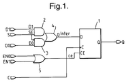
- Figure 1 shows the structure of a memory element used in an embodiment in accordance with the invention.
- the memory element is a D flip-flop 1 having a multiplexed input.
- the input has AND gates 2 and 3 and OR gates 4 and 5.
- Such multiplexing makes it possible to carry out the writing and the reading to the RAM in different directions, writing being done horizontally and reading vertically.
- D-type flip-flop 1 has a data input D, a clock input C, a clock enable input CE and an output Q.
- One, other or both inputs ENO and EN1 of OR gate 5 being HI results in a HI at input CE.
- Data on lines DO and D1 is input to D when line 5 is LO or HI respectively.
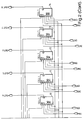
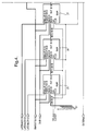
- FIG. 2 shows the structure of the memory, comprising memory elements utilising circuitry in accordance with the invention.
- Memory elements 6 - 14 are arranged so that there are 9 in each row. 30 such rows are placed vertically in succession, to form a RAM comprising 30 rows x 9 columns.
- One row at a time i.e. 9 bits at a time, is written into this memory. Since the data is transmitted to the receiver in serial form, it must be converted into parallel form prior to being input to the memory. Such a conversion is easy to implement using a simple well known transfer register.
- the writing into the memory is started from the bottom row, the address of which is 01 (HEX).
- Each memory element in a row has its DO data line connected to respective data lines 0 to 8 of data lines IN8(8:0), and its D1 data line connected to respective data lines 0 to 8 of data bus IN (0...8).
- Column enable lines EN0 to EN8 are input to respective EN1 inputs of memory elements (1) in each row and respective row enable lines ROW-ENAB are input to EN0 inputs of memory elements in respective rows.
- Clock and select signals are connected to the C and S inputs respectively of each memory element.
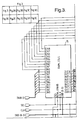
- FIG 3 shows an embodiment of the invention in which the RAM comprises 10 RAM cells 15...24 sequentially connected together via their output buses OUT(0...8) and input data buses IN(0...8).
- Each RAM cell 15...24 has input to its clock enable inputs EN(0...8) enable signals ENAOUT (8:0).
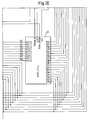
- Figure 4 shows three RAMS, 25, 26, 27 coupled together via their output and input buses OUT (8...0), IN (8...0) respectively.
- the output bus OUT (8...0) of RAM 27 is coupled via selecting logic 28...39 under control of respective enable lines ENAOUT (8:0) to D type flip flop 40 such that data stored in the RAMS 25, 26, 27 is output serially.
- the non-active LO state of the multiplexing selection line SEL is asserted.
- data lines DO are active for each memory element; i.e. data bus IN8 (8:0).
- Respective rows are then selected by known addressing methods. The addressing method activates the ROW-ENAB line of a first row, enabling the clock inputs of the memory elements of that row. Then the first 9 bits from the series to parallel converter are clocked in parallel into that row.
- Memory elements 15 - 24 are disposed such that the i th memory element 15 - 24 of each row, i.e. the write input of memory element 15 - 24, is wired to the i th bit of the series to parallel converter.
- the ROW-ENAB line of the row corresponding to this new address is activated and the ROW-ENAB line of the previous row is deactivated. Again, the arrival of 9 bits is waited for, whereafter this nine-bit word is clocked into the memory elements. This procedure is continued until all of the 30 rows have been loaded.
- each column of the RAM is addressed using enable signals ENAOUT (8:0) which are coupled to clock enabling lines ENO...EN8 of memory cells in respective columns 0 to 8.
- the addressing method activates the signal EN0 first, thus enabling the clock input of the memory elements of column 0. Thereafter the data in the column (30 bits) is sequentially read from the column.
- the memory elements are coupled vertically in series so that, in reading out, an entire 30 bit-word is obtained with 30 clock cycles from the RAM, with the MSB first.
- the entire 30-bit column is clocked out by using the CLK signal.
- a new address is selected, which activates a new ENO .. EN7 line, and the word corresponding to this address can be read out.
- Either one or more RAMs described above can be used for deinterleaving.
- the other one is being unloaded, i.e. it is being read from simultaneously. If only one RAM is used, the memory is read into in the normal manner until even the last row has been loaded. Thereafter, the memory is unloaded while the next 9 bits are being received. This, however, sets high speed requirements on the blocks subsequent to the deinterleaving.
- the generation of addresses is quite easy, since the rows and columns are loaded/unloaded in order.
- the address counters are set to zero.
- the desired next address is produced by clocking the address counters one step forward.
- the memory control is very easy, and it can be effected by using two address counters.
- a deinterleaving depth (30 x 9 bits) compatible with the ERMES system is discussed, but the same method can be used for implementing any depth of deinterleaving.
- the method according to the invention is very suitable for use in an ERMES paging system.
- deinterleaving can be implemented with very little address coding.
- the basic memory elements have multiplexed inputs. If these inputs are wired in the manner according to the invention, deinterleaving can be implemented in a simple manner.
- the invention is significant mainly when so high a speed is required in interleaving or deinterleaving that the processor in the device will not have time to carry out the operation through software.
- the method according to the invention speeds up the operation considerably.
Landscapes
- Physics & Mathematics (AREA)
- Engineering & Computer Science (AREA)
- Theoretical Computer Science (AREA)
- Mathematical Physics (AREA)
- General Engineering & Computer Science (AREA)
- General Physics & Mathematics (AREA)
- Error Detection And Correction (AREA)
Applications Claiming Priority (2)
| Application Number | Priority Date | Filing Date | Title |
|---|---|---|---|
| FI931648A FI93676C (fi) | 1993-04-13 | 1993-04-13 | Kytkentä deinterliivauksen toteuttamiseksi hakulaitejärjestelmässä |
| FI931648 | 1993-04-13 |
Publications (3)
| Publication Number | Publication Date |
|---|---|
| EP0624838A2 true EP0624838A2 (de) | 1994-11-17 |
| EP0624838A3 EP0624838A3 (de) | 1995-02-15 |
| EP0624838B1 EP0624838B1 (de) | 2001-10-17 |
Family
ID=8537727
Family Applications (1)
| Application Number | Title | Priority Date | Filing Date |
|---|---|---|---|
| EP94302614A Expired - Lifetime EP0624838B1 (de) | 1993-04-13 | 1994-04-13 | Vorrichtung und Verfahren zur Entschachtelung |
Country Status (4)
| Country | Link |
|---|---|
| EP (1) | EP0624838B1 (de) |
| DE (1) | DE69428624T2 (de) |
| FI (1) | FI93676C (de) |
| SG (1) | SG74545A1 (de) |
Family Cites Families (3)
| Publication number | Priority date | Publication date | Assignee | Title |
|---|---|---|---|---|
| GB2160685B (en) * | 1984-06-02 | 1987-09-03 | Int Computers Ltd | Data reorganisation apparatus |
| US5063533A (en) * | 1989-04-10 | 1991-11-05 | Motorola, Inc. | Reconfigurable deinterleaver/interleaver for block oriented data |
| FR2657739B1 (fr) * | 1990-01-26 | 1992-05-07 | Sgc Thomson Microelectronics Sa | Serialiseur/deserialiseur. |
-
1993
- 1993-04-13 FI FI931648A patent/FI93676C/fi not_active IP Right Cessation
-
1994
- 1994-04-13 EP EP94302614A patent/EP0624838B1/de not_active Expired - Lifetime
- 1994-04-13 SG SG1996001544A patent/SG74545A1/en unknown
- 1994-04-13 DE DE69428624T patent/DE69428624T2/de not_active Expired - Fee Related
Also Published As
| Publication number | Publication date |
|---|---|
| FI93676B (fi) | 1995-01-31 |
| DE69428624D1 (de) | 2001-11-22 |
| FI931648L (fi) | 1994-10-14 |
| DE69428624T2 (de) | 2002-06-20 |
| SG74545A1 (en) | 2000-08-22 |
| FI93676C (fi) | 1995-05-10 |
| HK1001035A1 (en) | 1998-05-15 |
| EP0624838B1 (de) | 2001-10-17 |
| EP0624838A3 (de) | 1995-02-15 |
| FI931648A0 (fi) | 1993-04-13 |
Similar Documents
| Publication | Publication Date | Title |
|---|---|---|
| US4069970A (en) | Data access circuit for a memory array | |
| EP0473275B1 (de) | Speichersteuerungseinheit und Speichereinheit | |
| US5010516A (en) | Content addressable memory | |
| US4899316A (en) | Semiconductor memory device having serial writing scheme | |
| US4183095A (en) | High density memory device | |
| JP3992757B2 (ja) | マイクロプロセッサと同期するメモリ、及びデータプロセッサ、同期メモリ、周辺装置とシステムクロックを含むシステム | |
| US4672614A (en) | Semiconductor memory device with parallel addressing and data-correcting functions | |
| JPH0524596B2 (de) | ||
| CA1258910A (en) | Page mode operation of main system memory in a medium scale computer | |
| EP0454836B1 (de) | System zur integrität der speicherdaten | |
| KR0158696B1 (ko) | 에러 검출 및 보정 방법 | |
| US4800535A (en) | Interleaved memory addressing system and method using a parity signal | |
| EP0290042A2 (de) | Speicherschaltung mit serieller Adressierung | |
| EP0096779A2 (de) | Mehrbit Fehlerstreuanordnung um einen fehlertoleranten Halbleiterspeicher zu beliefern | |
| US4852059A (en) | Content addressable memory | |
| EP0624838A2 (de) | Vorrichtung und Verfahren zur Entschachtelung | |
| HK1001035B (en) | Apparatus and method for deinterleaving | |
| EP0153015A2 (de) | Integrierte Wafer-Scale-Schaltungen | |
| EP0588129A2 (de) | Halbleiterspeicheranordnung | |
| EP0924707A2 (de) | Synchrone dynamische Direktzugriffspeicherachitektur für seriellen Burstmodus | |
| GB1197418A (en) | Data Storage Apparatus | |
| US5146456A (en) | Computer system with distributed content-addressable memory modules compatible with cito transmission | |
| EP0341887A2 (de) | Rasterpufferspeicher | |
| US5485597A (en) | A CCD array memory device achieving high speed accessing by writing and reading data through a cache memory | |
| US5373464A (en) | CCD array memory device having dual, independent clocks of differing speeds |
Legal Events
| Date | Code | Title | Description |
|---|---|---|---|
| PUAI | Public reference made under article 153(3) epc to a published international application that has entered the european phase |
Free format text: ORIGINAL CODE: 0009012 |
|
| AK | Designated contracting states |
Kind code of ref document: A2 Designated state(s): DE FR GB SE |
|
| PUAL | Search report despatched |
Free format text: ORIGINAL CODE: 0009013 |
|
| AK | Designated contracting states |
Kind code of ref document: A3 Designated state(s): DE FR GB SE |
|
| 17P | Request for examination filed |
Effective date: 19950816 |
|
| 17Q | First examination report despatched |
Effective date: 19981117 |
|
| GRAG | Despatch of communication of intention to grant |
Free format text: ORIGINAL CODE: EPIDOS AGRA |
|
| GRAG | Despatch of communication of intention to grant |
Free format text: ORIGINAL CODE: EPIDOS AGRA |
|
| GRAH | Despatch of communication of intention to grant a patent |
Free format text: ORIGINAL CODE: EPIDOS IGRA |
|
| GRAH | Despatch of communication of intention to grant a patent |
Free format text: ORIGINAL CODE: EPIDOS IGRA |
|
| GRAA | (expected) grant |
Free format text: ORIGINAL CODE: 0009210 |
|
| AK | Designated contracting states |
Kind code of ref document: B1 Designated state(s): DE FR GB SE |
|
| REF | Corresponds to: |
Ref document number: 69428624 Country of ref document: DE Date of ref document: 20011122 |
|
| ET | Fr: translation filed | ||
| REG | Reference to a national code |
Ref country code: GB Ref legal event code: IF02 |
|
| RAP2 | Party data changed (patent owner data changed or rights of a patent transferred) |
Owner name: NOKIA CORPORATION |
|
| REG | Reference to a national code |
Ref country code: GB Ref legal event code: 732E |
|
| PLBE | No opposition filed within time limit |
Free format text: ORIGINAL CODE: 0009261 |
|
| STAA | Information on the status of an ep patent application or granted ep patent |
Free format text: STATUS: NO OPPOSITION FILED WITHIN TIME LIMIT |
|
| 26N | No opposition filed | ||
| PGFP | Annual fee paid to national office [announced via postgrant information from national office to epo] |
Ref country code: DE Payment date: 20060406 Year of fee payment: 13 |
|
| PG25 | Lapsed in a contracting state [announced via postgrant information from national office to epo] |
Ref country code: DE Free format text: LAPSE BECAUSE OF NON-PAYMENT OF DUE FEES Effective date: 20071101 |
|
| PGFP | Annual fee paid to national office [announced via postgrant information from national office to epo] |
Ref country code: GB Payment date: 20100325 Year of fee payment: 17 |
|
| PGFP | Annual fee paid to national office [announced via postgrant information from national office to epo] |
Ref country code: FR Payment date: 20100521 Year of fee payment: 17 |
|
| PGFP | Annual fee paid to national office [announced via postgrant information from national office to epo] |
Ref country code: SE Payment date: 20100409 Year of fee payment: 17 |
|
| REG | Reference to a national code |
Ref country code: SE Ref legal event code: EUG |
|
| GBPC | Gb: european patent ceased through non-payment of renewal fee |
Effective date: 20110413 |
|
| REG | Reference to a national code |
Ref country code: FR Ref legal event code: ST Effective date: 20111230 |
|
| PG25 | Lapsed in a contracting state [announced via postgrant information from national office to epo] |
Ref country code: FR Free format text: LAPSE BECAUSE OF NON-PAYMENT OF DUE FEES Effective date: 20110502 |
|
| PG25 | Lapsed in a contracting state [announced via postgrant information from national office to epo] |
Ref country code: GB Free format text: LAPSE BECAUSE OF NON-PAYMENT OF DUE FEES Effective date: 20110413 |
|
| PG25 | Lapsed in a contracting state [announced via postgrant information from national office to epo] |
Ref country code: SE Free format text: LAPSE BECAUSE OF NON-PAYMENT OF DUE FEES Effective date: 20110414 |