EP0621961B1 - Optical modulation device - Google Patents
Optical modulation device Download PDFInfo
- Publication number
- EP0621961B1 EP0621961B1 EP93902391A EP93902391A EP0621961B1 EP 0621961 B1 EP0621961 B1 EP 0621961B1 EP 93902391 A EP93902391 A EP 93902391A EP 93902391 A EP93902391 A EP 93902391A EP 0621961 B1 EP0621961 B1 EP 0621961B1
- Authority
- EP
- European Patent Office
- Prior art keywords
- plates
- secured
- plate
- liquid crystal
- spacer members
- Prior art date
- Legal status (The legal status is an assumption and is not a legal conclusion. Google has not performed a legal analysis and makes no representation as to the accuracy of the status listed.)
- Expired - Lifetime
Links
- 230000003287 optical effect Effects 0.000 title claims abstract description 12
- 125000006850 spacer group Chemical group 0.000 claims abstract description 50
- 239000000463 material Substances 0.000 claims abstract description 42
- 239000004973 liquid crystal related substance Substances 0.000 claims abstract description 29
- 239000005262 ferroelectric liquid crystals (FLCs) Substances 0.000 claims abstract description 8
- 230000004888 barrier function Effects 0.000 claims description 11
- 238000000926 separation method Methods 0.000 abstract description 4
- 230000000712 assembly Effects 0.000 description 10
- 238000000429 assembly Methods 0.000 description 10
- 230000000694 effects Effects 0.000 description 5
- 230000035515 penetration Effects 0.000 description 4
- 238000004891 communication Methods 0.000 description 3
- 238000010276 construction Methods 0.000 description 3
- 238000005728 strengthening Methods 0.000 description 3
- 230000002939 deleterious effect Effects 0.000 description 2
- 239000007787 solid Substances 0.000 description 2
- 239000004593 Epoxy Substances 0.000 description 1
- 239000004642 Polyimide Substances 0.000 description 1
- 238000003491 array Methods 0.000 description 1
- 230000009286 beneficial effect Effects 0.000 description 1
- 230000005540 biological transmission Effects 0.000 description 1
- 238000010586 diagram Methods 0.000 description 1
- 230000002708 enhancing effect Effects 0.000 description 1
- 239000011521 glass Substances 0.000 description 1
- AMGQUBHHOARCQH-UHFFFAOYSA-N indium;oxotin Chemical compound [In].[Sn]=O AMGQUBHHOARCQH-UHFFFAOYSA-N 0.000 description 1
- 238000004519 manufacturing process Methods 0.000 description 1
- 238000000034 method Methods 0.000 description 1
- 230000004048 modification Effects 0.000 description 1
- 238000012986 modification Methods 0.000 description 1
- 230000000704 physical effect Effects 0.000 description 1
- 229920001721 polyimide Polymers 0.000 description 1
Images

Classifications
-
- G—PHYSICS
- G02—OPTICS
- G02F—OPTICAL DEVICES OR ARRANGEMENTS FOR THE CONTROL OF LIGHT BY MODIFICATION OF THE OPTICAL PROPERTIES OF THE MEDIA OF THE ELEMENTS INVOLVED THEREIN; NON-LINEAR OPTICS; FREQUENCY-CHANGING OF LIGHT; OPTICAL LOGIC ELEMENTS; OPTICAL ANALOGUE/DIGITAL CONVERTERS
- G02F1/00—Devices or arrangements for the control of the intensity, colour, phase, polarisation or direction of light arriving from an independent light source, e.g. switching, gating or modulating; Non-linear optics
- G02F1/01—Devices or arrangements for the control of the intensity, colour, phase, polarisation or direction of light arriving from an independent light source, e.g. switching, gating or modulating; Non-linear optics for the control of the intensity, phase, polarisation or colour
- G02F1/13—Devices or arrangements for the control of the intensity, colour, phase, polarisation or direction of light arriving from an independent light source, e.g. switching, gating or modulating; Non-linear optics for the control of the intensity, phase, polarisation or colour based on liquid crystals, e.g. single liquid crystal display cells
- G02F1/133—Constructional arrangements; Operation of liquid crystal cells; Circuit arrangements
- G02F1/1333—Constructional arrangements; Manufacturing methods
- G02F1/1339—Gaskets; Spacers; Sealing of cells
- G02F1/13394—Gaskets; Spacers; Sealing of cells spacers regularly patterned on the cell subtrate, e.g. walls, pillars
-
- G—PHYSICS
- G02—OPTICS
- G02F—OPTICAL DEVICES OR ARRANGEMENTS FOR THE CONTROL OF LIGHT BY MODIFICATION OF THE OPTICAL PROPERTIES OF THE MEDIA OF THE ELEMENTS INVOLVED THEREIN; NON-LINEAR OPTICS; FREQUENCY-CHANGING OF LIGHT; OPTICAL LOGIC ELEMENTS; OPTICAL ANALOGUE/DIGITAL CONVERTERS
- G02F1/00—Devices or arrangements for the control of the intensity, colour, phase, polarisation or direction of light arriving from an independent light source, e.g. switching, gating or modulating; Non-linear optics
- G02F1/01—Devices or arrangements for the control of the intensity, colour, phase, polarisation or direction of light arriving from an independent light source, e.g. switching, gating or modulating; Non-linear optics for the control of the intensity, phase, polarisation or colour
- G02F1/13—Devices or arrangements for the control of the intensity, colour, phase, polarisation or direction of light arriving from an independent light source, e.g. switching, gating or modulating; Non-linear optics for the control of the intensity, phase, polarisation or colour based on liquid crystals, e.g. single liquid crystal display cells
- G02F1/137—Devices or arrangements for the control of the intensity, colour, phase, polarisation or direction of light arriving from an independent light source, e.g. switching, gating or modulating; Non-linear optics for the control of the intensity, phase, polarisation or colour based on liquid crystals, e.g. single liquid crystal display cells characterised by the electro-optical or magneto-optical effect, e.g. field-induced phase transition, orientation effect, guest-host interaction or dynamic scattering
- G02F1/139—Devices or arrangements for the control of the intensity, colour, phase, polarisation or direction of light arriving from an independent light source, e.g. switching, gating or modulating; Non-linear optics for the control of the intensity, phase, polarisation or colour based on liquid crystals, e.g. single liquid crystal display cells characterised by the electro-optical or magneto-optical effect, e.g. field-induced phase transition, orientation effect, guest-host interaction or dynamic scattering based on orientation effects in which the liquid crystal remains transparent
- G02F1/141—Devices or arrangements for the control of the intensity, colour, phase, polarisation or direction of light arriving from an independent light source, e.g. switching, gating or modulating; Non-linear optics for the control of the intensity, phase, polarisation or colour based on liquid crystals, e.g. single liquid crystal display cells characterised by the electro-optical or magneto-optical effect, e.g. field-induced phase transition, orientation effect, guest-host interaction or dynamic scattering based on orientation effects in which the liquid crystal remains transparent using ferroelectric liquid crystals
Definitions
- This invention relates to an optical modulation device including first and second optically transmissive parallel plates having a ferroelectric liquid crystal material sandwiched therebetween, a plurality of spacer members, each secured to a said plate, being located between said plates for maintaining spacing between said plates at a predetermined value, said spacer members defining substantially parallel liquid crystal material-containing channels extending parallel to the plates.
- a device of the above general kind is known, for example, from GB-B-2157451 and US-A-4763995.
- the facing surfaces of the two plates are normally provided with respective arrays of optically transmissive electrodes, for example, mutually orthogonal grids of electrodes, by means of which portions of the liquid crystal material can be selectively addressed.
- Such addressing enables optical properties of selected portions of the material to be changed. If the assembly of the two plates is positioned between crossed polarisers, the said addressing can result in modification of the optical transmissivity of selected areas of the resulting device, thereby enabling it to be used, for example, as a television display device.
- the spacer members take the form of parallel solid walls all of which are secured to one plate and extend from one side of the plate to the other.
- the walls of the device disclosed therein serve the additional purpose of improving monodomain formability in the liquid crystal material, and to this end they are oriented parallel with or perpendicular to a monaxial orientation treatment (conventionally a rubbing treatment) which has been applied to the face of at least one of the two plates contacting the liquid crystal material.
- Devices of the general kind specified in the first paragraph can be subjected to substantial temperature variations. This can give rise to problems in some cases if spacer members of the kind disclosed in the above-identified patents are employed. In particular differences in the thermal expansion coefficients of the materials of the spacer members and the plate to which they are secured may give rise to disruption of the structural integrity of the device.
- Devices of the general kind specified in the first paragraph can, moreover, be subjected to mechanical deformation forces which cause parts of the liquid crystal material to move relative to other parts thereof. If the spacing between the plates is small and the liquid crystal material has a high viscosity this can result in changes in physical properties of parts of the material which have a deleterious effect on operation of the device and which can only be reversed with difficulty.
- the invention provides from one aspect an optical modulation device including first and second optically transmissive parallel plates which face and are spaced from each other, ferroelectric liquid crystal material sandwiched between said plates, and a plurality of spacer members, each secured to a said plate, located between said plates for maintaining the spacing between the plates at a predetermined value, said spacer members being arranged to form elongate barriers to flow of liquid crystal material, which barriers extend parallel to each other and to the plates, characterized in that the barriers are segmented with each segment consisting of one said spacer member, and the spaces between the spacer members forming the successive segments of each barrier are sufficiently small that liquid crystal material voids are present within them.
- the invention also provides, from a second aspect an optical modulation device including first and second optically transmissive parallel plates which face and are spaced from each other, ferroelectric liquid crystal material sandwiched between said plates, and a plurality of spacer members, each secured to a said plate, located between said plates for maintaining the spacing members forming elongate strips which extend parallel to each other and to the plates and constitute barriers to flow of liquid crystal material, characterized in that each strip has an auxiliary strip associated with it, which auxiliary strip is secured to a said plate, runs parallel to but spaced from the strip with which it is associated and on the same side of the strip with which it is associated, and is of insufficient height to contact the plate other than that to which it is secured, the resulting gap between each auxiliary strip and the plate other than that to which it is secured being sufficiently small that liquid crystal material voids are present between each auxiliary strip and the strip with which it is associated.
- Sets of the spacer members may be each configured as successive spaced segments of a respective wall which runs between a said channel and an adjacent said channel, spaces between the segments constituting the said cavities. If this is the case segmented versions of the solid walls of GB-B-2157451 can in effect be obtained. It has been found that such segmented versions can have an adequate spacing and strengthening effect without causing the device to suffer unduly from the effects of temperature changes. Moreover, if the members of a first subset of a said set are secured to the first plate and the members of a second subset of the said set are secured to the second plate these members can be arranged so that the members of the two subsets form an interdigitated structure.
- the resulting voids will be, in general, more compressible than the liquid crystal material. Presence of such voids can result in a reduction in bulk flow of the liquid crystal material should the device be subjected to mechanical deformation forces, and hence in a reduction in the deleterious effect of such forces on the operation of the device referred to hereinbefore. Such a beneficial effect can be obtained, for example, if the cavities are constituted by spaces between successive wall segments as set forth above, or otherwise.
- a preferred construction in this respect is one in which the spacer members are in the form of walls each of which runs between a said channel and an adjacent said channel, each said wall having an auxiliary wall associated therewith, which auxiliary wall is secured to a said plate, is spaced from the wall with which it is associated and runs between the said channel and adjacent channel, the space between the two walls forming a said cavity and being at least partly devoid of said ferroelectric liquid crystal material.
- each auxiliary wall is preferably of lesser height than the wall with which it is associated, so that a gap exists between its top and the said plate other than that to which it is secured.
- each auxiliary wall of lesser height than the wall with which it is associated can facilitate communication between the space containing the liquid crystal material and the space between the two walls, although in some circumstances useful communication might conceivably be obtained if the two walls are of the same height.
- Each auxiliary wall and the wall with which it is associated may be secured to the same said plate, although preferably each said auxiliary wall is secured to one said plate and the wall with which it is associated is secured to the other said plate.
- a plurality of further spacer members are located in said channels, said further spacer members adhering to both of said plates. Provision of such further spacer members can increase the mechanical strength of the device.
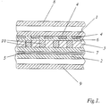
- an optical modulation device part of which is shown diagrammatically edge-on, comprises first and second optically transparent parallel plates 1 and 2, for example of glass, having a ferroelectric liquid crystal material 3 sandwiched between them. Selected portions of the liquid crystal material can be addressed in known manner by means of a grid of parallel transparent electrodes 4, for example of indium tin oxide, positioned on the inner surface of the plate 1, and a similar but orthogonal grid of parallel transparent electrodes 5 positioned on the inner surface of the plate 2.
- the electrodes 4 and 5 are separated from the material 3 in known manner by barrier-and-alignment layers 6 and 7 respectively.
- These spacer members form segments of parallel walls which extend perpendicular to the plane of the paper and thereby define parallel channels, also extending perpendicular to the plane of the paper (and parallel to the plate assemblies 1,4,6 and 2,5,7), containing the liquid crystal material 3.
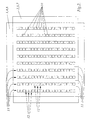
- spacer members 10 are shown diagrammatically in the plan view of Fig. 2, together with the channels 11 therebetween. As will be seen from Fig. 2 the spacer members 10 are substantially square. Spaces 12 between the successive spacer members 10 making up each wall 13 form cavities communicating with the channels 11. Preferably the spaces 12 are sufficiently small that surface forces prevent complete penetration thereof by the liquid crystal material 3.
- substantially equal numbers of the set of spacer members 10 which make up at least one and preferably each of the walls 13 are secured to the plate assembly 1,4,6 and to the plate assembly 2,5,7 respectively.
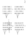
- This may be done, for example, by arranging that the spacer members 10 constituting the successive segments of each wall 13 are secured alternately to the plate assembly 1,4,6 and to the plate assembly 2,5,7, either as shown diagrammatically in Fig. 3 (a) or as shown diagrammatically in fig. 3b, in which Figures the shaded squares denote spacer members secured to one assembly and the open squares denote spacer members secured to the other assembly.
- pairs of adjacent spacer members constituting the successive segments of each wall may be secured alternately to the plate assembly 1,4,6 and to the plate assembly 2,5,7, either as shown diagrammatically in Fig. 3c or as shown diagrammatically in Fig. 3d.
- the segmented walls 13 formed by the spacers 10 are in all cases aligned with the gaps between successive electrodes 4. Although, as shown, respective walls are provided aligned with each successive such gap, this is not essential; respective walls may, for example, be provided aligned with only alternate ones of the successive such gaps.
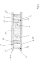
- Fig. 4 is a diagrammatic view, analogous to that of Fig. 1, of part of an alternative construction to those described so far with reference to Figs. 1 to 3.
- each spacer member 10 which is now in the form of a continuous wall extending perpendicular to the plane of the paper, has associated with it an auxiliary wall 14 which is also secured to one of the plate assemblies 1,4,6 and 2, 5, 7, preferably the other one of these assemblies to that to which the member 10 is secured, to facilitate manufacture.
- Each auxiliary wall 14 is spaced from, and is of lesser height than, the wall 10 with which it is associated so that a gap 15 exists between its top 16 and the other plate assembly (2,5,7) to that to which it is secured.
- This gap 15 forms a communication between the cavity 17 between the two walls and the adjacent liquid crystal material-containing channel 11.
- the gaps 15 are sufficiently small that surface forces and/or residual trapped gas prevent complete penetration of the liquid crystal material 3 into the cavities 15, 17.
- Fig. 5 is a diagrammatic plan view, analogous to those of Figs. 3a-3d, showing the members 10 of Fig. 4, together with their associated auxiliary walls 14, the shading of the walls 10 denoting that they are secured to one plate assembly 1,4,6 or 2,5,7, whereas the walls 14 are secured to the other.
- a further spacer member 18 is shown in dashed lines in Fig. 4, located in a channel 11.
- a plurality of such, substantially spherical, further spacer members may be provided in the various channels 11, if desired, this also being applicable to the embodiments described with reference to Figs. 1 to 3.
- the spacer member 18 is a so-called “sticky spacer” such as is available, for example, under the trade name "TORRAY”. These sticky spacers are initially in the form of partly cured epoxy spheres which are squashable.
- the spacer members 10, and the auxiliary walls 14 if present may conveniently be formed of polyimide which is spun on the appropriate surface of the relevant plate assembly 1,4,6 or 2,5,7 to provide a layer of appropriate thickness. Appropriate parts of this layer are then removed using a photoresist-employing process to leave the correctly-positioned spacer members 10, and/or auxiliary walls 14 if present.
- the two plate assemblies together with the secured spacer members 10, and auxiliary walls 14 if present, are then brought together, an edge seal is cured, and the resulting structure is vacuum back-filled with the liquid crystal material 3.
- the length direction of the walls 13 may take any desired angle with the rubbing direction(s) of the alignment layers 6 and 7 of Fig. 1.
- the spacing between the two plates 1,4,6 and 2,5,7 was 1.5 ⁇ m
- the widths of the channels 11 were 90 ⁇ m
- the widths of the walls 13 were 20 ⁇ m as were the lengths of the successive segments thereof
- the separations between the successive spacer members 10 constituting these segments were 5 ⁇ m.
- liquid crystal material used for example one of those obtainable from Messrs. Merck, had a viscosity of less than 10 -2 Nm -2 s at the filling temperature.
Landscapes
- Physics & Mathematics (AREA)
- Nonlinear Science (AREA)
- Mathematical Physics (AREA)
- Chemical & Material Sciences (AREA)
- Crystallography & Structural Chemistry (AREA)
- General Physics & Mathematics (AREA)
- Optics & Photonics (AREA)
- Liquid Crystal (AREA)
Abstract
Description
Claims (5)
- An optical modulation device including first (1) and second (2) optically transmissive parallel plates which face and are spaced from each other, ferroelectric liquid crystal material (3) sandwiched between said plates, and a plurality of spacer members (10), each secured to a said plate, located between said plates for maintaining the spacing between the plates at a predetermined value, said spacer members being arranged to form elongate barriers (13) to flow of liquid crystal material, which barriers extend parallel to each other and to the plates, characterized in that the barriers are segmented with each segment consisting of one said spacer member, and the spaces (12) between the spacer members forming the successive segments of each barrier are sufficiently small that liquid crystal material voids are present within them.
- A device as claimed in Claim 1, wherein the members of a first subset of a respective set of spacer members (10) forming the segments of each barrier are secured to the first plate (1) and the members of a second subset of said set are secured to the second plate (2) so that the two subsets form an interdigitated structure.
- An optical modulation device including first (1) and second (2) optically transmissive parallel plates which face and are spaced from each other, ferroelectric liquid crystal material (3) sandwiched between said plates, and a plurality of spacer members (10), each secured to a said plate, located between said plates for maintaining the spacing between the plates at a predetermined value, said spacer members forming elongate strips (10) which extend parallel to each other and to the plates and constitute barriers to flow of liquid crystal material, characterized in that each strip has an auxiliary strip (14) associated with it, which auxiliary strip is secured to a said plate, runs parallel to but spaced from the strip (10) with which it is associated and on the same side of the strip with which it is associated, and is of insufficient height to contact the plate other than that to which it is secured, the resulting gap (15) between each auxiliary strip (14) and the plate other than that to which it is secured being sufficiently small that liquid crystal material voids are present between each auxiliary strip and the strip with which it is associated.
- A device as claimed in Claim 3, wherein each auxiliary strip (14) is secured to one said plate and the strip (10) with which it is associated is secured to the other said plate.
- A device as claimed in any preceding claim, including a plurality of further spacer members (18) adhering to both of said plates (1, 2).
Applications Claiming Priority (3)
| Application Number | Priority Date | Filing Date | Title |
|---|---|---|---|
| GB929200839A GB9200839D0 (en) | 1992-01-15 | 1992-01-15 | Optical modulation device |
| GB9200839 | 1992-01-15 | ||
| PCT/GB1993/000091 WO1993014437A1 (en) | 1992-01-15 | 1993-01-15 | Optical modulation device |
Publications (2)
| Publication Number | Publication Date |
|---|---|
| EP0621961A1 EP0621961A1 (en) | 1994-11-02 |
| EP0621961B1 true EP0621961B1 (en) | 1998-04-15 |
Family
ID=10708649
Family Applications (1)
| Application Number | Title | Priority Date | Filing Date |
|---|---|---|---|
| EP93902391A Expired - Lifetime EP0621961B1 (en) | 1992-01-15 | 1993-01-15 | Optical modulation device |
Country Status (8)
| Country | Link |
|---|---|
| US (1) | US5459598A (en) |
| EP (1) | EP0621961B1 (en) |
| JP (1) | JP3333513B2 (en) |
| CA (1) | CA2127997C (en) |
| DE (1) | DE69318006T2 (en) |
| ES (1) | ES2114603T3 (en) |
| GB (1) | GB9200839D0 (en) |
| WO (1) | WO1993014437A1 (en) |
Families Citing this family (44)
| Publication number | Priority date | Publication date | Assignee | Title |
|---|---|---|---|---|
| KR0161387B1 (en) * | 1995-01-27 | 1999-01-15 | 윤종용 | Tft lcd and its fabrication method |
| US5838414A (en) * | 1995-12-30 | 1998-11-17 | Samsung Display Devices Co., Ltd. | LCD device with improved resilient adhesive spacers |
| US5871559A (en) * | 1996-12-10 | 1999-02-16 | Bloom; Cary | Arrangement for automated fabrication of fiber optic devices |
| US6000858A (en) * | 1996-07-12 | 1999-12-14 | Bloom; Cary | Apparatus for, and method of, forming a low stress tight fit of an optical fiber to an external element |
| US5971629A (en) * | 1996-07-12 | 1999-10-26 | Bloom; Cary | Apparatus and method bonding optical fiber and/or device to external element using compliant material interface |
| US5815619A (en) * | 1996-12-10 | 1998-09-29 | Bloom; Cary | Fiber optic connector hermetically terminated |
| US5805757A (en) * | 1996-12-10 | 1998-09-08 | Bloom; Cary | Apparatus and method for preserving optical characteristics of a fiber optic device |
| GB2347006B (en) * | 1996-07-26 | 2000-10-04 | Sharp Kk | Liquid crystal device |
| US5948134A (en) * | 1996-09-24 | 1999-09-07 | Bloom; Cary | Apparatus for forming a fiber optic coupler by dynamically adjusting pulling speed and heat intensity |
| US5764348A (en) * | 1996-10-01 | 1998-06-09 | Bloom; Cary | Optical switching assembly for testing fiber optic devices |
| US6177985B1 (en) | 1996-10-01 | 2001-01-23 | Cary Bloom | Apparatus and method for testing optical fiber system components |
| JPH10123534A (en) * | 1996-10-23 | 1998-05-15 | Toshiba Corp | Liquid crystal display device |
| US6003341A (en) * | 1996-12-10 | 1999-12-21 | Bloom; Cary | Device for making fiber couplers automatically |
| US6074101A (en) * | 1996-12-10 | 2000-06-13 | Bloom; Cary | Apparatus for, and method of, forming a low stress tight fit of an optical fiber to an external element |
| US5917975A (en) * | 1996-12-10 | 1999-06-29 | Bloom; Cary | Apparatus for, and method of, forming a low stress tight fit of an optical fiber to an external element |
| US5831710A (en) * | 1997-02-06 | 1998-11-03 | International Business Machines Corporation | Liquid crystal display |
| JP3903130B2 (en) * | 1997-03-11 | 2007-04-11 | フジコピアン株式会社 | Thermal transfer material for dot spacer formation |
| US6141072A (en) * | 1997-04-04 | 2000-10-31 | Georgia Tech Research Corporation | System and method for efficient manufacturing of liquid crystal displays |
| US5953087A (en) * | 1997-04-11 | 1999-09-14 | Cambridge Research & Instrumentation Inc. | Apparatus for stress relieving liquid crystal displays |
| US6465268B2 (en) | 1997-05-22 | 2002-10-15 | Semiconductor Energy Laboratory Co., Ltd. | Method of manufacturing an electro-optical device |
| US5766694A (en) * | 1997-05-29 | 1998-06-16 | Univ Kent State Ohio | Method for forming uniformly-spaced plastic substrate liquid crystal displays |
| US5929960A (en) * | 1997-10-17 | 1999-07-27 | Kent State University | Method for forming liquid crystal display cell walls using a patterned electric field |
| US6219126B1 (en) * | 1998-11-20 | 2001-04-17 | International Business Machines Corporation | Panel assembly for liquid crystal displays having a barrier fillet and an adhesive fillet in the periphery |
| US6348959B1 (en) * | 1998-12-21 | 2002-02-19 | Philips Electronics North America Corporation | Reflective LCD with dark borders |
| JP3098515B1 (en) * | 1999-08-13 | 2000-10-16 | インターナショナル・ビジネス・マシーンズ・コーポレ−ション | Liquid crystal display device, liquid crystal display device with narrow frame, and method of manufacturing liquid crystal display device |
| JP4132528B2 (en) * | 2000-01-14 | 2008-08-13 | シャープ株式会社 | Manufacturing method of liquid crystal display device |
| JP4118484B2 (en) | 2000-03-06 | 2008-07-16 | 株式会社半導体エネルギー研究所 | Method for manufacturing semiconductor device |
| JP2001257350A (en) | 2000-03-08 | 2001-09-21 | Semiconductor Energy Lab Co Ltd | Semiconductor device and manufacturing method thereof |
| JP4700160B2 (en) | 2000-03-13 | 2011-06-15 | 株式会社半導体エネルギー研究所 | Semiconductor device |
| JP4683688B2 (en) | 2000-03-16 | 2011-05-18 | 株式会社半導体エネルギー研究所 | Method for manufacturing liquid crystal display device |
| JP4393662B2 (en) | 2000-03-17 | 2010-01-06 | 株式会社半導体エネルギー研究所 | Method for manufacturing liquid crystal display device |
| JP4785229B2 (en) | 2000-05-09 | 2011-10-05 | 株式会社半導体エネルギー研究所 | Method for manufacturing semiconductor device |
| JP3992922B2 (en) * | 2000-11-27 | 2007-10-17 | シャープ株式会社 | LIQUID CRYSTAL DISPLAY SUBSTRATE, ITS MANUFACTURING METHOD, AND LIQUID CRYSTAL DISPLAY DEVICE EQUIPPED WITH THE SAME |
| JP3680730B2 (en) * | 2000-12-08 | 2005-08-10 | 株式会社日立製作所 | Liquid crystal display |
| TW554221B (en) * | 2001-01-09 | 2003-09-21 | Matsushita Electric Industrial Co Ltd | Liquid crystal display device and manufacturing method thereof |
| TWI285279B (en) * | 2001-06-14 | 2007-08-11 | Himax Tech Ltd | Liquid crystal display panel having sealant |
| JP3937304B2 (en) * | 2002-01-10 | 2007-06-27 | 鹿児島日本電気株式会社 | Manufacturing method of liquid crystal display panel |
| JP4159910B2 (en) * | 2003-03-20 | 2008-10-01 | シャープ株式会社 | Liquid crystal display |
| KR100672650B1 (en) * | 2004-02-25 | 2007-01-24 | 엘지.필립스 엘시디 주식회사 | Liquid crystal display and manufacturing method thereof |
| US20060017876A1 (en) * | 2004-07-23 | 2006-01-26 | Molecular Imprints, Inc. | Displays and method for fabricating displays |
| JP2006350211A (en) * | 2005-06-20 | 2006-12-28 | Toshiba Matsushita Display Technology Co Ltd | Liquid crystal display device |
| US8134679B2 (en) * | 2006-09-11 | 2012-03-13 | Sharp Kabushiki Kaisha | Liquid crystal display device |
| US8179514B2 (en) * | 2006-10-05 | 2012-05-15 | Sharp Kabushiki Kaisha | Liquid crystal display device with first and second protruding walls surrounding spherical spacers |
| JP2012198544A (en) * | 2012-04-16 | 2012-10-18 | Semiconductor Energy Lab Co Ltd | Display device |
Family Cites Families (6)
| Publication number | Priority date | Publication date | Assignee | Title |
|---|---|---|---|---|
| CH651691A5 (en) * | 1981-07-24 | 1985-09-30 | Bbc Brown Boveri & Cie | DISPLAY DEVICE WITH LIQUID CRYSTAL AND METHOD FOR THE PRODUCTION THEREOF. |
| US4763995A (en) * | 1983-04-28 | 1988-08-16 | Canon Kabushiki Kaisha | Spacers with alignment effect and substrates having a weak alignment effect |
| JPS60188925A (en) * | 1984-03-09 | 1985-09-26 | Canon Inc | Manufacturing method of optical modulation element |
| US4688899A (en) * | 1984-07-27 | 1987-08-25 | Casio Computer Co., Ltd. | Dual-frequency, dielectric anisotropy liquid crystal display |
| JPS62502147A (en) * | 1985-03-05 | 1987-08-20 | アメリカン テレフオン アンド テレグラフ カムパニ− | Thin and uniform electro-optic display device |
| US4775225A (en) * | 1985-05-16 | 1988-10-04 | Canon Kabushiki Kaisha | Liquid crystal device having pillar spacers with small base periphery width in direction perpendicular to orientation treatment |
-
1992
- 1992-01-15 GB GB929200839A patent/GB9200839D0/en active Pending
-
1993
- 1993-01-15 CA CA002127997A patent/CA2127997C/en not_active Expired - Fee Related
- 1993-01-15 WO PCT/GB1993/000091 patent/WO1993014437A1/en not_active Ceased
- 1993-01-15 EP EP93902391A patent/EP0621961B1/en not_active Expired - Lifetime
- 1993-01-15 ES ES93902391T patent/ES2114603T3/en not_active Expired - Lifetime
- 1993-01-15 US US08/256,545 patent/US5459598A/en not_active Expired - Lifetime
- 1993-01-15 DE DE69318006T patent/DE69318006T2/en not_active Expired - Lifetime
- 1993-01-15 JP JP51229193A patent/JP3333513B2/en not_active Expired - Fee Related
Also Published As
| Publication number | Publication date |
|---|---|
| ES2114603T3 (en) | 1998-06-01 |
| US5459598A (en) | 1995-10-17 |
| GB9200839D0 (en) | 1992-03-11 |
| WO1993014437A1 (en) | 1993-07-22 |
| JPH07502839A (en) | 1995-03-23 |
| CA2127997C (en) | 2002-08-13 |
| DE69318006T2 (en) | 1998-12-03 |
| EP0621961A1 (en) | 1994-11-02 |
| JP3333513B2 (en) | 2002-10-15 |
| DE69318006D1 (en) | 1998-05-20 |
| CA2127997A1 (en) | 1993-07-22 |
Similar Documents
| Publication | Publication Date | Title |
|---|---|---|
| US5459598A (en) | Optical modulation device with liquid crystal voids formed by the spacer arrangements | |
| US5838414A (en) | LCD device with improved resilient adhesive spacers | |
| US4728176A (en) | Ferroelectric liquid crystal device with metallic auxiliary electrodes provided adjacent to the transparent electrodes | |
| EP0525473B1 (en) | Liquid crystal cell | |
| US6118510A (en) | Liquid crystal device | |
| DE69230451T2 (en) | Ferroelectric liquid crystal panel and process for its manufacture | |
| DE2703177C2 (en) | Scoreboard | |
| US4924243A (en) | Method for manufacturing liquid crystal device with spacers formed by printing | |
| DE102019212536A1 (en) | Liquid crystal device and spacers for liquid crystal applications | |
| US5039205A (en) | Liquid crystal electro-optical device | |
| EP0536680A2 (en) | Liquid crystal device and liquid crystal injection method | |
| JP2002202512A (en) | Liquid crystal display device and manufacturing method thereof | |
| KR100575324B1 (en) | Liquid-crystal display device | |
| EP0623838B1 (en) | Plasma-addressed liquid crystal display device | |
| DE3224264A1 (en) | DISPLAY DEVICE WITH LIQUID CRYSTAL AND METHOD FOR THE PRODUCTION THEREOF | |
| KR20070050741A (en) | LCD and its manufacturing method | |
| JP2939836B2 (en) | Liquid crystal display device | |
| JP2000321588A (en) | Liquid crystal display | |
| US5513024A (en) | Liquid crystal display and method for making the same | |
| JP4414061B2 (en) | Liquid crystal display device and manufacturing method thereof | |
| KR101030536B1 (en) | Liquid crystal display mask and pattern spacer manufacturing method using same | |
| KR100672649B1 (en) | Liquid crystal display | |
| DE3343746A1 (en) | LIQUID CRYSTAL CELL AND METHOD FOR THE PRODUCTION THEREOF | |
| KR0144989B1 (en) | Stereoscopic Liquid Crystal Display Element | |
| WO1996014651A1 (en) | Plasma display panel |
Legal Events
| Date | Code | Title | Description |
|---|---|---|---|
| PUAI | Public reference made under article 153(3) epc to a published international application that has entered the european phase |
Free format text: ORIGINAL CODE: 0009012 |
|
| 17P | Request for examination filed |
Effective date: 19940725 |
|
| AK | Designated contracting states |
Kind code of ref document: A1 Designated state(s): DE ES FR GB IT NL |
|
| 17Q | First examination report despatched |
Effective date: 19951228 |
|
| RAP1 | Party data changed (applicant data changed or rights of an application transferred) |
Owner name: CENTRAL RESEARCH LABORATORIES LIMITED |
|
| GRAG | Despatch of communication of intention to grant |
Free format text: ORIGINAL CODE: EPIDOS AGRA |
|
| GRAG | Despatch of communication of intention to grant |
Free format text: ORIGINAL CODE: EPIDOS AGRA |
|
| GRAH | Despatch of communication of intention to grant a patent |
Free format text: ORIGINAL CODE: EPIDOS IGRA |
|
| GRAH | Despatch of communication of intention to grant a patent |
Free format text: ORIGINAL CODE: EPIDOS IGRA |
|
| GRAA | (expected) grant |
Free format text: ORIGINAL CODE: 0009210 |
|
| AK | Designated contracting states |
Kind code of ref document: B1 Designated state(s): DE ES FR GB IT NL |
|
| ITF | It: translation for a ep patent filed | ||
| REF | Corresponds to: |
Ref document number: 69318006 Country of ref document: DE Date of ref document: 19980520 |
|
| REG | Reference to a national code |
Ref country code: ES Ref legal event code: FG2A Ref document number: 2114603 Country of ref document: ES Kind code of ref document: T3 |
|
| ET | Fr: translation filed | ||
| PLBE | No opposition filed within time limit |
Free format text: ORIGINAL CODE: 0009261 |
|
| STAA | Information on the status of an ep patent application or granted ep patent |
Free format text: STATUS: NO OPPOSITION FILED WITHIN TIME LIMIT |
|
| 26N | No opposition filed | ||
| REG | Reference to a national code |
Ref country code: GB Ref legal event code: IF02 |
|
| PGFP | Annual fee paid to national office [announced via postgrant information from national office to epo] |
Ref country code: ES Payment date: 20040123 Year of fee payment: 12 |
|
| PG25 | Lapsed in a contracting state [announced via postgrant information from national office to epo] |
Ref country code: ES Free format text: LAPSE BECAUSE OF NON-PAYMENT OF DUE FEES Effective date: 20050117 |
|
| REG | Reference to a national code |
Ref country code: ES Ref legal event code: FD2A Effective date: 20050117 |
|
| PGFP | Annual fee paid to national office [announced via postgrant information from national office to epo] |
Ref country code: IT Payment date: 20070616 Year of fee payment: 15 |
|
| PG25 | Lapsed in a contracting state [announced via postgrant information from national office to epo] |
Ref country code: IT Free format text: LAPSE BECAUSE OF NON-PAYMENT OF DUE FEES Effective date: 20080115 |
|
| PGFP | Annual fee paid to national office [announced via postgrant information from national office to epo] |
Ref country code: FR Payment date: 20100223 Year of fee payment: 18 |
|
| PGFP | Annual fee paid to national office [announced via postgrant information from national office to epo] |
Ref country code: GB Payment date: 20100113 Year of fee payment: 18 Ref country code: DE Payment date: 20100121 Year of fee payment: 18 |
|
| PGFP | Annual fee paid to national office [announced via postgrant information from national office to epo] |
Ref country code: NL Payment date: 20100118 Year of fee payment: 18 |
|
| REG | Reference to a national code |
Ref country code: NL Ref legal event code: V1 Effective date: 20110801 |
|
| GBPC | Gb: european patent ceased through non-payment of renewal fee |
Effective date: 20110115 |
|
| REG | Reference to a national code |
Ref country code: FR Ref legal event code: ST Effective date: 20110930 |
|
| PG25 | Lapsed in a contracting state [announced via postgrant information from national office to epo] |
Ref country code: FR Free format text: LAPSE BECAUSE OF NON-PAYMENT OF DUE FEES Effective date: 20110131 |
|
| PG25 | Lapsed in a contracting state [announced via postgrant information from national office to epo] |
Ref country code: GB Free format text: LAPSE BECAUSE OF NON-PAYMENT OF DUE FEES Effective date: 20110115 |
|
| REG | Reference to a national code |
Ref country code: DE Ref legal event code: R119 Ref document number: 69318006 Country of ref document: DE Effective date: 20110802 |
|
| PG25 | Lapsed in a contracting state [announced via postgrant information from national office to epo] |
Ref country code: NL Free format text: LAPSE BECAUSE OF NON-PAYMENT OF DUE FEES Effective date: 20110801 |
|
| PG25 | Lapsed in a contracting state [announced via postgrant information from national office to epo] |
Ref country code: DE Free format text: LAPSE BECAUSE OF NON-PAYMENT OF DUE FEES Effective date: 20110802 |