EP0616468A2 - Video signal processing system - Google Patents
Video signal processing system Download PDFInfo
- Publication number
- EP0616468A2 EP0616468A2 EP94104233A EP94104233A EP0616468A2 EP 0616468 A2 EP0616468 A2 EP 0616468A2 EP 94104233 A EP94104233 A EP 94104233A EP 94104233 A EP94104233 A EP 94104233A EP 0616468 A2 EP0616468 A2 EP 0616468A2
- Authority
- EP
- European Patent Office
- Prior art keywords
- signal
- auxiliary
- circuit
- edtv
- video signal
- Prior art date
- Legal status (The legal status is an assumption and is not a legal conclusion. Google has not performed a legal analysis and makes no representation as to the accuracy of the status listed.)
- Withdrawn
Links
Images


Classifications
-
- H—ELECTRICITY
- H04—ELECTRIC COMMUNICATION TECHNIQUE
- H04N—PICTORIAL COMMUNICATION, e.g. TELEVISION
- H04N7/00—Television systems
- H04N7/007—Systems with supplementary picture signal insertion during a portion of the active part of a television signal, e.g. during top and bottom lines in a HDTV letter-box system
-
- H—ELECTRICITY
- H04—ELECTRIC COMMUNICATION TECHNIQUE
- H04N—PICTORIAL COMMUNICATION, e.g. TELEVISION
- H04N9/00—Details of colour television systems
- H04N9/79—Processing of colour television signals in connection with recording
- H04N9/80—Transformation of the television signal for recording, e.g. modulation, frequency changing; Inverse transformation for playback
- H04N9/82—Transformation of the television signal for recording, e.g. modulation, frequency changing; Inverse transformation for playback the individual colour picture signal components being recorded simultaneously only
- H04N9/83—Transformation of the television signal for recording, e.g. modulation, frequency changing; Inverse transformation for playback the individual colour picture signal components being recorded simultaneously only the recorded chrominance signal occupying a frequency band under the frequency band of the recorded brightness signal
- H04N9/832—Transformation of the television signal for recording, e.g. modulation, frequency changing; Inverse transformation for playback the individual colour picture signal components being recorded simultaneously only the recorded chrominance signal occupying a frequency band under the frequency band of the recorded brightness signal using an increased bandwidth for the luminance or the chrominance signal
Definitions
- the present invention relates to a video signal processing system.
- Fig. 4 which is useful to explain an image of a letter box system
- Fig. 5 which shows a signal format for the EDTV (Extended Definition Television) system.
- EDTV Extended Definition Television
- TV receiver television receiver
- One of such transmission systems is the so-called letter box system in which, when an image is displayed on a screen of a conventional TV receiver, black portions are displayed on an upper region and a lower region of the displayed picture and the image information is displayed on a vertical center with an aspect ratio of 16 : 9, as shown in Fig.
- auxiliary signals dd1 and dd2 corresponding to two vertical high frequency components or two horizontal high frequency components or a vertical high frequency component and a horizontal high frequency component are inserted into the black portions of the image.
- cc indicates a picture signal of image information.
- modulation scheme have been considered to be so-called the VSB-modulation (vestigial side band modulation) obtained by restricting its carrier or digital encoding.
- an EDTV identification signal bb is inserted into a predetermined scanning line within a vertical blanking period as shown in Fig. 5. And, when the auxiliary signals dd1 and dd2 are absent, a constant black level is present in the auxiliary signal periods dd11 and dd22.
- EDTV signal An example of such EDTV signal is the "PAL plus" system which is under consideration in Europe.
- VTR magnetic video signal recording and reproducing apparatus
- Japanese Patent Application 4-30146/1992 titled "Magnetic Video Signal Recording Apparatus" and assigned to the same assignee of the present application proposes a VTR for recording a video signal containing a time-division multiplexed picture signal representing an image information and an auxiliary signal related to the picture signal, which comprises a first filter for separating a luminance signal from the video signal, a demodulator for converting the auxiliary signal into a base-band frequency without passing the first filter, a luminance signal recording circuit which FM-modulates an output of the demodulator when at least the auxiliary signal is present, otherwise FM modulates the luminance signal, second filter for separating a color signal from the video signal and a color signal recording circuit including a conversion of the color signal into a frequency range lower than that of the luminance signal, whereby the output of the luminance signal recording circuit and the output of the color signal recording circuit are frequency-multiplexed and recorded on the tape.
- the reproduced video signal (reproduced as not a correct EDTV signal but a normal video signal), is displayable on a screen of a conventional TV receiver having a screen aspect ratio of 4 : 3 as such that the EDTV signal hh' shown in Fig. 2(A) presents its base band auxiliary signals as black portions corresponding to the upper and lower portions of the displayed picture.
- the base band auxiliary signal in the reproduced video signal has a large amplitude centered at a DC reference level which is higher than the level of the normally modulated auxiliary signals dd1 and dd2 centered at the black level.
- the luminance of the upper and lower portions of the displayed image, which correspond to the base band auxiliary signal do not become complete black but relatively bright gray and too conspicuous, thus the center portion of the image to be watched is not highlighted but relatively dim.
- Another and specific object of the invention is to provide a video signal processing system for processing various types of video signals including an EDTV signal containing a picture signal indicative of image information and an auxiliary signal related to the picture signal, the auxiliary signal being time-division multiplexed with the picture signal, the system comprises an auxiliary signal period detection means for outputting a detection signal by detecting a period of the auxiliary signal residing in a base-band frequency when the EDTV signal inputted to the system contains the auxiliary signal being in the base-band frequency and muting means for muting the EDTV signal in the period of the auxiliary signal in the base-band frequency in response to the detection signal.
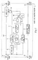
- FIG. 1 is a block diagram of an embodiment of a video signal processing system according to the present invention
- Fig. 2 is a waveform of EDTV signal and a related time charts showing an operation of the video signal processing system
- Fig. 3 is a schematic diagram showing an application of the video signal processing system according to the present invention.
- the video signal processing system is capable of outputting the EDTV signal of which a base band auxiliary signal (unmodulated or unencoded auxiliary signal) is substantially removed when an EDTV signal with auxiliary signal in the base band frequency is inputted thereto, thereby disturbance on the displayed picture on a screen of a connected conventional TV receiver due to the auxiliary signal is prevented from appearing.
- a base band auxiliary signal unmodulated or unencoded auxiliary signal
- the video signal processing system 1 processes a video signal including a picture signal indicative of an image information and an EDTV signal hh time-division multiplexed with auxiliary signals dd1 and dd2 related to the picture signal cc and an identification signal bb.
- a video signal processing system 1 comprises an auxiliary signal period detection circuit for outputting a detection signal "g" obtained by detecting auxiliary signal periods dd11 and dd22 of the base band auxiliary signals dd1' and dd2' which are obtained by converting frequencies of the auxiliary signals dd1 and dd2 into the base band frequency when the EDTV signal hh' including the base band auxiliary signals dd1' and dd2' are inputted, and a mute circuit 4 for substantially muting the EDTV signal hh' including the base band auxiliary signals ddl' and dd2' during the auxiliary signal periods dd11 and dd22 on the basis of the auxiliary signal detection signal "g".
- the video signal processing system 1 is constituted with the mute circuit 4, a synchronizing signal separating circuit 6, a timing pulse generator circuit 7, AND circuits 8 and 11, an identification signal (hereinafter referred to as "ID") gate circuit 9, an ID content identifying circuit 10, a DC reference level detector circuit 12, a base band auxiliary signal ID removing circuit 14 and a switch SW.
- ID identification signal
- Reference numerals 2 and 5 denote a video signal input terminal and a video signal output terminal respectively, and 13 and 15 denote base band auxiliary signal ID input and output terminals respectively.
- the auxiliary signal period detection circuit is constituted with the synchronizing signal separating circuit 6, the timing pulse generator circuit 7, the AND circuits 8 and 11, the identification signal gate circuit 9, the identification signal content discriminating circuit 10, the DC reference level detection circuit 12, the base band auxiliary signal ID removing circuit 14 and the switch SW.
- a luminance signal obtained by separating it from a color signal in frequency by passing a composite video signal through a band pass filter which is not shown or a luminance signal of a group of color and luminance signals (so-called the Y/C separated signals), one of which may be a part of the EDTV signal hh', is supplied to a video signal input terminal 2.
- the EDTV signal hh' in Fig. 2(A) is supplied to the video signal input terminal 2
- this input signal is supplied to the mute circuit 4, the synchronizing signal separating circuit 6, the identification signal gate circuit 9 and the DC reference level detection circuit 12.
- the synchronizing signal separating circuit 6 separates a horizontal and vertical synchronizing signals from the EDTV signal hh' and supplies them to the timing pulse generator circuit 7.
- the timing pulse generator circuit 7 produces, on the basis of the horizontal and vertical synchronizing signals from the synchronizing signal separating circuit 6, a pulse "b" (Fig. 2(B)) which is in “H” level only during the auxiliary signal periods dd11 and dd22 where the base band auxiliary signals dd1' and dd2' are present in a period of 1 field of the EDTV signal hh', and produces a pulse "c" (Fig. 2(C)) which is in "H” level only during a period in which a DC reference level aa is present in a period of 1 field of the EDTV signal hh', and produces a pulse dl as a logical sum of the pulses "b" and "c".
- a pulse “d” (Fig. 2(D)) which is a logical product of the pulse dl and a pulse being in "H” level in a period other than a horizontal retrace period.
- the pulse “d” indicates a mute period for muting the EDTV signal hh'.
- the timing pulse generator circuit 7 produces a pulse d2 which is in "H” level only for a period in which the identification signal bb is present n 1 field of the EDTV signal hh' and supplies it to the identification signal gate circuit 9 and supplies the pulse "c" to the DC reference level detection circuit 12.
- the identification signal gate circuit 9 extracts, in response to the pulse d2 supplied from the timing pulse generator circuit 7, the identification signal bb of the EDTV signal hh' supplied from the video signal input terminar 2, and supplies it to the identification signal content discrimination circuit 10.
- the identification signal content discrimination circuit 10 identifies an information content of the identification signal bb supplied from the identification signal gate circuit 9 and supplies a pulse "e" (Fig. 2(E)) which becomes in "H” level when it identifies a presence of the information related to the EDTV signal, to one of inputs of the AND circuit 11.
- the DC reference level detection circuit 12 makes a comparator (not shown) operable for a period in which the pulse "c" from the timing pulse generator circuit 7 is in “H” level and supplies a pulse "f" (Fig. 2(F)) to the other input of the AND circuit 11 when it detects a presence of the DC reference level aa of the EDTV signal hh' from the video signal input terminal 2 which is higher than a predetermined level (for example, the DC reference level).
- the AND circuit 11 supplies a pulse "h” which is a logical product of the pulse "e” from the identification signal content discrimination circuit 10 and the pulse “f” from the DC reference level detection circuit 12, to a contact A of the switch SW.
- the switch SW is a manual switch operable externally and includes three contacts A, B and C and a movable contact.
- the contact A is supplied with the pulse "h" from the AND circuit 11, the contact B is continuously grounded (“L” level) and the contact C is continuously supplied with a voltage Vcc ("H" level).
- the EDTV signal being muted in the auxiliary signal periods dd11 and dd22 of the EDTV signal hh' can be supplied to the video signal output terminal 5. Therefore, to obtain the same function, it is possible to substitute the switch SW having the three fixed contacts A, B and C with a switch SW having two fixed contacts B and C, by doing so, the identification signal gate circuit 9, the identification signal content discrimination circuit 10, the AND circuit 11 and the DC reference level detection circuit 12 can be omitted as a modifieation of the video signal processing system 1.
- a VTR20 (Fig. 3) records the auxiliary signal of the EDTV signal by converting its auxiliary signal into a base band frequency, and reproduces the recorded signal with an ID signal (the ID) for indicating the auxiliary signal being in the base band frequency and supplies the ID to a predetermined pin of a multi-pin connector, it is also necessary to remove the ID.
- the ID from the VTR 20 is supplied to the base band auxiliary signal ID input terminal 13 through the predetermined pin.
- the base band auxiliary signal ID removing circuit 14 supplies a signal of which the ID supplied to the base band auxiliary signal ID input terminal 13 is removed, to a TV receiver 30 (Fig. 3) through the terminal 15.
- the ID removing circuit 14 is provided with a low-pass filter (not shown) having a cut-off frequency low enough to suppress an AC component of the ID, or a comparator (not shown) which outputs the DC signal by comparing an intermediate level of the inputted ID, which is not subjected to the low level square wave.
- a low-pass filter not shown
- a comparator not shown
- the DC signal indicative of another identification content is outputted to the terminal 15.
- the ID removing circuit 14 is provided with a level converter circuit which converts the "H” level ID to an "L” level signal, so that the low level signal having no function as the base band auxiliary signal ID, is outputted to the terminal 15.
- the receiver 30 is the EDTV compatible receiver and is connected to the video signal processing system 1, it is possible to prevent an erroneous operation of the EDTV compatible receiver due to a supply of the ID with no base band auxiliary signal accompanied. Otherwise, the operation of the EDTV compatible receiver would be fooled under such circumstance.
- the mute circuit 4 mutes the auxiliary signal periods dd11 and dd22 of the EDTV signal hh'.
- auxiliary signal periods dd11 and dd22 it is possible to replace them with a constant level luminance signal, a signal indicative of a constant color, an image corresponding to the picture signal cc stored in a memory, etc., or a display of date (that is, substantially muting the base band auxiliary signal).
- a constant level luminance signal a signal indicative of a constant color
- a display of date that is, substantially muting the base band auxiliary signal.
- the video signal processing system resides in a video signal processing system for performing a signal processing a video signal including an EDTV signal which contains a picture signal indicative of image information and an auxiliary signal related to and time-division multiplexed with the picture signal, comprising the auxiliary signal period detection circuit for outputting an auxiliary signal period signal obtained by detecting an auxiliary signal period related to a base band auxiliary signal from an EDTV signal including the base band auxiliary signal obtained by converting a frequency of the auxiliary signal into base band frequency and the mute circuit for substantially muting the EDTV signal including the base band auxiliary signal during the auxiliary signal period on the basis of the auxiliary signal detection signal.
- an EDTV signal obtained by substantially removing the base band auxiliary signal when the EDTV signal containing the same is inputted so that, in displaying an image on a screen of a conventional TV receiver connected to the present processing system, the upper and lower portions of the screen which correspond to the base band auxiliary signal become complete black, high lighting the center portion of the displayed image which is to be watched.
Landscapes
- Engineering & Computer Science (AREA)
- Multimedia (AREA)
- Signal Processing (AREA)
- Television Systems (AREA)
Abstract
Description
- The present invention relates to a video signal processing system.
- Prior arts will be described with reference to Fig. 4 which is useful to explain an image of a letter box system and Fig. 5 which shows a signal format for the EDTV (Extended Definition Television) system.
- A transmission system for transmitting a high quality image having a display screen aspect ratio of 16 : 9, which is compatible with a conventional "television receiver" (hereinafter referred to as "TV receiver") having a screen aspect ratio of 4 : 3, has been studied. One of such transmission systems is the so-called letter box system in which, when an image is displayed on a screen of a conventional TV receiver, black portions are displayed on an upper region and a lower region of the displayed picture and the image information is displayed on a vertical center with an aspect ratio of 16 : 9, as shown in Fig. 5 and, when it is displayed on a screen of an EDTV receiver which is capable of reproducing an image having an aspect ratio of 16 : 9 filling the same aspect ratio screen, two auxiliary signals dd1 and dd2 corresponding to two vertical high frequency components or two horizontal high frequency components or a vertical high frequency component and a horizontal high frequency component are inserted into the black portions of the image. In Fig. 5, cc indicates a picture signal of image information. For the auxiliary signals dd1 and dd2. modulation scheme have been considered to be so-called the VSB-modulation (vestigial side band modulation) obtained by restricting its carrier or digital encoding. These signals are illustrated in Fig. 5 and will be referred to as the EDTV signal hereinafter. In order to identify such EDTV signal, an EDTV identification signal bb is inserted into a predetermined scanning line within a vertical blanking period as shown in Fig. 5. And, when the auxiliary signals dd1 and dd2 are absent, a constant black level is present in the auxiliary signal periods dd11 and dd22.
- An example of such EDTV signal is the "PAL plus" system which is under consideration in Europe.
- When such EDTV signal is to be recorded and reproduced in a conventional magnetic video signal recording and reproducing apparatus (referred to as "VTR" hereinafter), it pauses a problem that the auxiliary signals dd1 and dd2 of the EDTV signal can not be decoded by a decoder for obtaining high quality image due to the following problems (1) to (3) for reasons that in such a conventional VTR, the input EDTV signal is simply regarded as a normal TV signal thus is not properly processed therein.
- (1) The auxiliary signals dd1 and dd2 are not always having line correlation and thus a portion of the auxiliary signals dd1 and dd2 having no line correlation is removed by a comb filter provided for separating a luminance (Y) signal and a color signal. Therefore, a degradation of the auxiliary signals dd1 and dd2 at an output of the comb filter may occur.
- (2) When the auxiliary signals dd1 and dd2 are VSB (Vestigial Side Band) modulated signals, it is necessary, in reproducing operation, to reproduce a carrier which tracks a jitter frequency caused and contained in a video signal reproduced from the conventional VTR. Therefore, it is impossible to accurately reproduce the VSB modulated signal without using a complicated time base correction. Further, since VSB modulated signal usually requires a wide band transmission system capable of transmitting a high frequency carrier, it is impossible to accurately record and reproduce it unless a wide band VTR is used.
- (3) When the auxiliary signals dd1 and dd2 are digitally encoded signals, an error correction code attaching circuit and an error correction circuit are necessary in recording and reproducing such signals. Further, since it is necessary to reproduce a clock signal for decoding purpose, such VTR must become complicated.
- In order to solve the problems (1) to (3), Japanese Patent Application 4-30146/1992 titled "Magnetic Video Signal Recording Apparatus" and assigned to the same assignee of the present application proposes a VTR for recording a video signal containing a time-division multiplexed picture signal representing an image information and an auxiliary signal related to the picture signal, which comprises a first filter for separating a luminance signal from the video signal, a demodulator for converting the auxiliary signal into a base-band frequency without passing the first filter, a luminance signal recording circuit which FM-modulates an output of the demodulator when at least the auxiliary signal is present, otherwise FM modulates the luminance signal, second filter for separating a color signal from the video signal and a color signal recording circuit including a conversion of the color signal into a frequency range lower than that of the luminance signal, whereby the output of the luminance signal recording circuit and the output of the color signal recording circuit are frequency-multiplexed and recorded on the tape.
- When a video signal recorded on a recording medium by the above proposed VTR, is reproduced by a conventional VTR of helical scan type having a conventional reproducing circuit which is not complementary to the recording circuit of the proposed VTR, the reproduced video signal (reproduced as not a correct EDTV signal but a normal video signal), is displayable on a screen of a conventional TV receiver having a screen aspect ratio of 4 : 3 as such that the EDTV signal hh' shown in Fig. 2(A) presents its base band auxiliary signals as black portions corresponding to the upper and lower portions of the displayed picture.
- However, since the base band auxiliary signal in the reproduced video signal has a large amplitude centered at a DC reference level which is higher than the level of the normally modulated auxiliary signals dd1 and dd2 centered at the black level. the luminance of the upper and lower portions of the displayed image, which correspond to the base band auxiliary signal do not become complete black but relatively bright gray and too conspicuous, thus the center portion of the image to be watched is not highlighted but relatively dim.
- Accordingly, it is a general object of the present invention to solve the aforementioned problems.
- Another and specific object of the invention is to provide a video signal processing system for processing various types of video signals including an EDTV signal containing a picture signal indicative of image information and an auxiliary signal related to the picture signal, the auxiliary signal being time-division multiplexed with the picture signal, the system comprises an auxiliary signal period detection means for outputting a detection signal by detecting a period of the auxiliary signal residing in a base-band frequency when the EDTV signal inputted to the system contains the auxiliary signal being in the base-band frequency and muting means for muting the EDTV signal in the period of the auxiliary signal in the base-band frequency in response to the detection signal.
-
- Fig. 1 is a block diagram of an embodiment of a video signal processing system according to the present invention;
- Fig. 2 is a waveform of EDTV signal and related time charts showing an operation of the video signal processing system;
- Fig. 3 is a schematic diagram showing an application of the video signal processing system according to the present invention;
- Fig. 4 is a figure explaining a letter box system; and
- Fig. 5 is a figure explaining an EDTV signal.
- A video signal processing system according to the present invention will be described with reference to Figs.1 to 3. Fig. 1 is a block diagram of an embodiment of a video signal processing system according to the present invention, Fig. 2 is a waveform of EDTV signal and a related time charts showing an operation of the video signal processing system, and Fig. 3 is a schematic diagram showing an application of the video signal processing system according to the present invention.
- The video signal processing system according to the present invention is capable of outputting the EDTV signal of which a base band auxiliary signal (unmodulated or unencoded auxiliary signal) is substantially removed when an EDTV signal with auxiliary signal in the base band frequency is inputted thereto, thereby disturbance on the displayed picture on a screen of a connected conventional TV receiver due to the auxiliary signal is prevented from appearing.
- As shown in Figs. 1 and 2, the video
signal processing system 1 according to the present invention processes a video signal including a picture signal indicative of an image information and an EDTV signal hh time-division multiplexed with auxiliary signals dd1 and dd2 related to the picture signal cc and an identification signal bb. - A video
signal processing system 1 comprises an auxiliary signal period detection circuit for outputting a detection signal "g" obtained by detecting auxiliary signal periods dd11 and dd22 of the base band auxiliary signals dd1' and dd2' which are obtained by converting frequencies of the auxiliary signals dd1 and dd2 into the base band frequency when the EDTV signal hh' including the base band auxiliary signals dd1' and dd2' are inputted, and amute circuit 4 for substantially muting the EDTV signal hh' including the base band auxiliary signals ddl' and dd2' during the auxiliary signal periods dd11 and dd22 on the basis of the auxiliary signal detection signal "g". - In Fig. 1, the video
signal processing system 1 is constituted with themute circuit 4, a synchronizing signal separating circuit 6, a timingpulse generator circuit 7, ANDcircuits 8 and 11, an identification signal (hereinafter referred to as "ID")gate circuit 9, an IDcontent identifying circuit 10, a DC referencelevel detector circuit 12, a base band auxiliary signalID removing circuit 14 and a switch SW.Reference numerals - The auxiliary signal period detection circuit is constituted with the synchronizing signal separating circuit 6, the timing
pulse generator circuit 7, theAND circuits 8 and 11, the identificationsignal gate circuit 9, the identification signal contentdiscriminating circuit 10, the DC referencelevel detection circuit 12, the base band auxiliary signalID removing circuit 14 and the switch SW. - An operation of the video
signal processing system 1 will be described. A luminance signal obtained by separating it from a color signal in frequency by passing a composite video signal through a band pass filter which is not shown or a luminance signal of a group of color and luminance signals (so-called the Y/C separated signals), one of which may be a part of the EDTV signal hh', is supplied to a videosignal input terminal 2. In case that the EDTV signal hh' in Fig. 2(A) is supplied to the videosignal input terminal 2, this input signal is supplied to themute circuit 4, the synchronizing signal separating circuit 6, the identificationsignal gate circuit 9 and the DC referencelevel detection circuit 12. - The synchronizing signal separating circuit 6 separates a horizontal and vertical synchronizing signals from the EDTV signal hh' and supplies them to the timing
pulse generator circuit 7. - The timing
pulse generator circuit 7 produces, on the basis of the horizontal and vertical synchronizing signals from the synchronizing signal separating circuit 6, a pulse "b" (Fig. 2(B)) which is in "H" level only during the auxiliary signal periods dd11 and dd22 where the base band auxiliary signals dd1' and dd2' are present in a period of 1 field of the EDTV signal hh', and produces a pulse "c" (Fig. 2(C)) which is in "H" level only during a period in which a DC reference level aa is present in a period of 1 field of the EDTV signal hh', and produces a pulse dl as a logical sum of the pulses "b" and "c". Further, it outputs to one of inputs of the AND circuit 8a, a pulse "d" (Fig. 2(D)) which is a logical product of the pulse dl and a pulse being in "H" level in a period other than a horizontal retrace period. The pulse "d" indicates a mute period for muting the EDTV signal hh'. At the same timing as this pulse "d", the timingpulse generator circuit 7 produces a pulse d2 which is in "H" level only for a period in which the identification signal bb ispresent n 1 field of the EDTV signal hh' and supplies it to the identificationsignal gate circuit 9 and supplies the pulse "c" to the DC referencelevel detection circuit 12. - The identification
signal gate circuit 9 extracts, in response to the pulse d2 supplied from the timingpulse generator circuit 7, the identification signal bb of the EDTV signal hh' supplied from the videosignal input terminar 2, and supplies it to the identification signalcontent discrimination circuit 10. - The identification signal
content discrimination circuit 10 identifies an information content of the identification signal bb supplied from the identificationsignal gate circuit 9 and supplies a pulse "e" (Fig. 2(E)) which becomes in "H" level when it identifies a presence of the information related to the EDTV signal, to one of inputs of theAND circuit 11. - The DC reference
level detection circuit 12 makes a comparator (not shown) operable for a period in which the pulse "c" from the timingpulse generator circuit 7 is in "H" level and supplies a pulse "f" (Fig. 2(F)) to the other input of theAND circuit 11 when it detects a presence of the DC reference level aa of the EDTV signal hh' from the videosignal input terminal 2 which is higher than a predetermined level (for example, the DC reference level). - The
AND circuit 11 supplies a pulse "h" which is a logical product of the pulse "e" from the identification signalcontent discrimination circuit 10 and the pulse "f" from the DC referencelevel detection circuit 12, to a contact A of the switch SW. - The switch SW is a manual switch operable externally and includes three contacts A, B and C and a movable contact. The contact A is supplied with the pulse "h" from the
AND circuit 11, the contact B is continuously grounded ("L" level) and the contact C is continuously supplied with a voltage Vcc ("H" level). - (1) Case where the movable contact is switched- to the contact A.
The pulse "h" from theAND circuit 11 is supplied to the other input of the AND circuit 8. As a result, the AND circuit 8 can supply the detection signal "g" which is the logical product of the pulse d1 from the timingpulse generator circuit 7 and the pulse "h" from theAND circuit 11, to themute circuit 4 as a mute control signal. Themute circuit 4 mutes the input video signal during a time in which the detection signal "g" is in "H" level and blocks the input video signal from outputting in response to the detection signal "g". Thus. themute circuit 4 supplies the videosignal output terminal 5 with the EDTV signal hh' having the auxiliary signal periods dd11 and dd22 being muted. - (2) Case where the movable contact is switched to the contact B
A potential of "L" level is outputted to the other input terminal of the AND circuit 8. As a result, the output of the AD circuit 8 is kept at a "L" level, so that can not supply the detection signal "g" to themute circuit 4 as a mute control signal. Therefore, themute circuit 4 does not perform a mute operation for a period in which the detection signal "g" is in "L" level. Thus, themute circuit 4 supplies the EDTV signal hh' supplied thereto to the videosignal output terminal 5 as is. - (3) Case where the movable contact is switched to the contact C
A potential of "H" level is supplied to the other input terminal of the AND circuit 8. As a result, the AND circuit 8 supplies the detection signal "g" which is the logical product of the "H" level from the switch SW and the pulse dl from the timingpulse generator circuit 7, to themute circuit 4 as a mute control signal. Themute circuit 4 mutes the input video signal for a period in which the detection signal "g" is in "H" level and blocks the output signal to the videosignal output terminal 5. Accordingly, themute circuit 4 supplies the EDTV signal hh' being muted in the auxiliary signal periods dd11 and dd22. to the videosignal output terminal 5. - In either the case (1) in which the movable contact is switched to the contact A or the case (3) in which the movable contact is switched to the contact C, the EDTV signal being muted in the auxiliary signal periods dd11 and dd22 of the EDTV signal hh' can be supplied to the video
signal output terminal 5. Therefore, to obtain the same function, it is possible to substitute the switch SW having the three fixed contacts A, B and C with a switch SW having two fixed contacts B and C, by doing so, the identificationsignal gate circuit 9, the identification signalcontent discrimination circuit 10, the ANDcircuit 11 and the DC referencelevel detection circuit 12 can be omitted as a modifieation of the videosignal processing system 1. - In case that a VTR20 (Fig. 3) records the auxiliary signal of the EDTV signal by converting its auxiliary signal into a base band frequency, and reproduces the recorded signal with an ID signal (the ID) for indicating the auxiliary signal being in the base band frequency and supplies the ID to a predetermined pin of a multi-pin connector, it is also necessary to remove the ID.
- In this case, an output side of the predetermined pin of the multi-pin connector whose input side is connected to an output of the VTR20 with a signal cable, is connected to the base band auxiliary signal
ID input terminal 13. As a result, the ID from theVTR 20 is supplied to the base band auxiliary signalID input terminal 13 through the predetermined pin. - The base band auxiliary signal
ID removing circuit 14 supplies a signal of which the ID supplied to the base band auxiliary signalID input terminal 13 is removed, to a TV receiver 30 (Fig. 3) through the terminal 15. - For the ID which is a low level square wave signal superimposed with a DC signal indicative of another identification content, the
ID removing circuit 14 is provided with a low-pass filter (not shown) having a cut-off frequency low enough to suppress an AC component of the ID, or a comparator (not shown) which outputs the DC signal by comparing an intermediate level of the inputted ID, which is not subjected to the low level square wave. Thus, the DC signal indicative of another identification content is outputted to the terminal 15. - For the ID being "H" indicative of the base band auxiliary signal, the
ID removing circuit 14 is provided with a level converter circuit which converts the "H" level ID to an "L" level signal, so that the low level signal having no function as the base band auxiliary signal ID, is outputted to the terminal 15. - Accordingly, when the
receiver 30 is the EDTV compatible receiver and is connected to the videosignal processing system 1, it is possible to prevent an erroneous operation of the EDTV compatible receiver due to a supply of the ID with no base band auxiliary signal accompanied. Otherwise, the operation of the EDTV compatible receiver would be fooled under such circumstance. - In the described embodiment, the
mute circuit 4 mutes the auxiliary signal periods dd11 and dd22 of the EDTV signal hh'. Alternatively, instead of muting the auxiliary signal periods dd11 and dd22, it is possible to replace them with a constant level luminance signal, a signal indicative of a constant color, an image corresponding to the picture signal cc stored in a memory, etc., or a display of date (that is, substantially muting the base band auxiliary signal). In these signals, periods corresponding to the DC reference level aa are rewritten in black level. - As described hereinbefore, the video signal processing system according to the present invention resides in a video signal processing system for performing a signal processing a video signal including an EDTV signal which contains a picture signal indicative of image information and an auxiliary signal related to and time-division multiplexed with the picture signal, comprising the auxiliary signal period detection circuit for outputting an auxiliary signal period signal obtained by detecting an auxiliary signal period related to a base band auxiliary signal from an EDTV signal including the base band auxiliary signal obtained by converting a frequency of the auxiliary signal into base band frequency and the mute circuit for substantially muting the EDTV signal including the base band auxiliary signal during the auxiliary signal period on the basis of the auxiliary signal detection signal. Therefore, it is possible to output an EDTV signal obtained by substantially removing the base band auxiliary signal when the EDTV signal containing the same is inputted, so that, in displaying an image on a screen of a conventional TV receiver connected to the present processing system, the upper and lower portions of the screen which correspond to the base band auxiliary signal become complete black, high lighting the center portion of the displayed image which is to be watched.
Claims (1)
- A video signal processing system for processing various types of video signals including an EDTV signal containing a picture signal indicative of image information and an auxiliary signal related to the picture signal, the auxiliary signal being time-division multiplexed with the picture signal, comprising:
an auxiliary signal period detection means for outputting a detection signal by detecting a period of said auxiliary signal residing in a base-band frequency when said EDTV signal inputted to the video signal processing system contains said auxiliary signal being in the base-band frequency; and
muting means for muting said EDTV signal in said period of the auxiliary signal in the base-band frequency in response to said detection signal.
Applications Claiming Priority (2)
| Application Number | Priority Date | Filing Date | Title |
|---|---|---|---|
| JP84061/93 | 1993-03-18 | ||
| JP5084061A JPH06276491A (en) | 1993-03-18 | 1993-03-18 | Video signal processing circuit |
Publications (2)
| Publication Number | Publication Date |
|---|---|
| EP0616468A2 true EP0616468A2 (en) | 1994-09-21 |
| EP0616468A3 EP0616468A3 (en) | 1995-03-08 |
Family
ID=13819987
Family Applications (1)
| Application Number | Title | Priority Date | Filing Date |
|---|---|---|---|
| EP94104233A Withdrawn EP0616468A3 (en) | 1993-03-18 | 1994-03-17 | Video signal processing system. |
Country Status (2)
| Country | Link |
|---|---|
| EP (1) | EP0616468A3 (en) |
| JP (1) | JPH06276491A (en) |
Cited By (1)
| Publication number | Priority date | Publication date | Assignee | Title |
|---|---|---|---|---|
| WO2002001857A1 (en) * | 2000-06-28 | 2002-01-03 | Koninklijke Philips Electronics N.V. | System and method for a video display screen saver |
Citations (5)
| Publication number | Priority date | Publication date | Assignee | Title |
|---|---|---|---|---|
| EP0433687A2 (en) * | 1989-12-21 | 1991-06-26 | GRUNDIG E.M.V. Elektro-Mechanische Versuchsanstalt Max Grundig holländ. Stiftung & Co. KG. | Videorecorder for recording and playing back video signals transmitted with the letter-box method |
| WO1991011882A1 (en) * | 1990-01-30 | 1991-08-08 | Deutsche Thomson-Brandt Gmbh | Letter-box colour television system with compartmented additional information |
| GB2254977A (en) * | 1992-04-23 | 1992-10-21 | Philips Electronics Nv | Receiver for letterbox television signals |
| WO1992020193A1 (en) * | 1991-04-30 | 1992-11-12 | Grundig E.M.V. Elektro-Mechanische Versuchsanstalt Max Grundig Holländ. Stiftung & Co. Kg | Video recorder for the recording of video signals transmitted by the letterbox process |
| DE4128337A1 (en) * | 1991-08-27 | 1993-03-04 | Thomson Brandt Gmbh | METHOD AND DEVICE FOR DECODING IMAGE SIGNALS WITH ADDITIONAL INFORMATION |
Family Cites Families (3)
| Publication number | Priority date | Publication date | Assignee | Title |
|---|---|---|---|---|
| JPH05328251A (en) * | 1992-05-20 | 1993-12-10 | Matsushita Electric Ind Co Ltd | Television receiver |
| JPH06165136A (en) * | 1992-11-18 | 1994-06-10 | Hitachi Ltd | Television signal processor |
| JPH06233248A (en) * | 1993-02-01 | 1994-08-19 | Hitachi Ltd | Video signal processing circuit |
-
1993
- 1993-03-18 JP JP5084061A patent/JPH06276491A/en active Pending
-
1994
- 1994-03-17 EP EP94104233A patent/EP0616468A3/en not_active Withdrawn
Patent Citations (5)
| Publication number | Priority date | Publication date | Assignee | Title |
|---|---|---|---|---|
| EP0433687A2 (en) * | 1989-12-21 | 1991-06-26 | GRUNDIG E.M.V. Elektro-Mechanische Versuchsanstalt Max Grundig holländ. Stiftung & Co. KG. | Videorecorder for recording and playing back video signals transmitted with the letter-box method |
| WO1991011882A1 (en) * | 1990-01-30 | 1991-08-08 | Deutsche Thomson-Brandt Gmbh | Letter-box colour television system with compartmented additional information |
| WO1992020193A1 (en) * | 1991-04-30 | 1992-11-12 | Grundig E.M.V. Elektro-Mechanische Versuchsanstalt Max Grundig Holländ. Stiftung & Co. Kg | Video recorder for the recording of video signals transmitted by the letterbox process |
| DE4128337A1 (en) * | 1991-08-27 | 1993-03-04 | Thomson Brandt Gmbh | METHOD AND DEVICE FOR DECODING IMAGE SIGNALS WITH ADDITIONAL INFORMATION |
| GB2254977A (en) * | 1992-04-23 | 1992-10-21 | Philips Electronics Nv | Receiver for letterbox television signals |
Non-Patent Citations (1)
| Title |
|---|
| SMPTE JOURNAL, vol.101, no.11, November 1992, SCARSDALE, NY US pages 790 - 796 ITO ET AL. 'A DECODER FOR A LETTER-BOX-TYPE WIDE-ASPECT EDTV SYSTEM' * |
Cited By (1)
| Publication number | Priority date | Publication date | Assignee | Title |
|---|---|---|---|---|
| WO2002001857A1 (en) * | 2000-06-28 | 2002-01-03 | Koninklijke Philips Electronics N.V. | System and method for a video display screen saver |
Also Published As
| Publication number | Publication date |
|---|---|
| EP0616468A3 (en) | 1995-03-08 |
| JPH06276491A (en) | 1994-09-30 |
Similar Documents
| Publication | Publication Date | Title |
|---|---|---|
| EP0677959A1 (en) | Picture information detecting apparatus for a video signal | |
| EP0507614B1 (en) | Video recording and/or reproducing apparatus | |
| EP0472572B1 (en) | Data transmission in the active picture period | |
| KR930010360B1 (en) | Restoring circuit for corresponding signal | |
| JPH1198422A (en) | Video signal discrimination circuit | |
| EP0616468A2 (en) | Video signal processing system | |
| KR100201023B1 (en) | Television receiver inside an image registration reproduction apparatus | |
| JP3111078B2 (en) | Video recorder for recording video signals transmitted by the mailbox method | |
| EP0616469A2 (en) | Television signal processing system | |
| EP0668704A2 (en) | Video signal transmission system | |
| EP0377471A1 (en) | Digital recording and reproducing apparatus for muse signal | |
| EP0691792B1 (en) | Video signal recording and reproducing apparatus and video signal receiving apparatus capable of detecting kind of video signal | |
| JP2630872B2 (en) | Television receiver | |
| JPH09200684A (en) | Video/audio signal recording device | |
| EP0479610B1 (en) | Television receiver | |
| KR0186110B1 (en) | Interface circuit for pal-plus signal of a vcr | |
| KR0155693B1 (en) | Caption information recording reproducing apparatus and its method | |
| JPH06268967A (en) | Video signal recording and/or reproducing device | |
| KR100982679B1 (en) | Video apparatus | |
| KR100334546B1 (en) | Signal disposal circuit | |
| US5422728A (en) | Motion signal recording and reproducing circuit | |
| JP2944173B2 (en) | Television signal processor | |
| JPH02193468A (en) | Picture-in-picture processing circuit | |
| JP3524193B2 (en) | Wide aspect television | |
| JPH09149382A (en) | Identification signal processor |
Legal Events
| Date | Code | Title | Description |
|---|---|---|---|
| PUAI | Public reference made under article 153(3) epc to a published international application that has entered the european phase |
Free format text: ORIGINAL CODE: 0009012 |
|
| AK | Designated contracting states |
Kind code of ref document: A2 Designated state(s): DE FR GB |
|
| PUAL | Search report despatched |
Free format text: ORIGINAL CODE: 0009013 |
|
| AK | Designated contracting states |
Kind code of ref document: A3 Designated state(s): DE FR GB |
|
| 17P | Request for examination filed |
Effective date: 19950621 |
|
| 17Q | First examination report despatched |
Effective date: 19980629 |
|
| STAA | Information on the status of an ep patent application or granted ep patent |
Free format text: STATUS: THE APPLICATION IS DEEMED TO BE WITHDRAWN |
|
| 18D | Application deemed to be withdrawn |
Effective date: 19981110 |