EP0615580B1 - Ignition system with variable primary voltage limitation and defect diagnosis - Google Patents
Ignition system with variable primary voltage limitation and defect diagnosis Download PDFInfo
- Publication number
- EP0615580B1 EP0615580B1 EP93918954A EP93918954A EP0615580B1 EP 0615580 B1 EP0615580 B1 EP 0615580B1 EP 93918954 A EP93918954 A EP 93918954A EP 93918954 A EP93918954 A EP 93918954A EP 0615580 B1 EP0615580 B1 EP 0615580B1
- Authority
- EP
- European Patent Office
- Prior art keywords
- voltage
- ignition
- primary
- ignition system
- primary winding
- Prior art date
- Legal status (The legal status is an assumption and is not a legal conclusion. Google has not performed a legal analysis and makes no representation as to the accuracy of the status listed.)
- Expired - Lifetime
Links
Images

Classifications
-
- F—MECHANICAL ENGINEERING; LIGHTING; HEATING; WEAPONS; BLASTING
- F02—COMBUSTION ENGINES; HOT-GAS OR COMBUSTION-PRODUCT ENGINE PLANTS
- F02P—IGNITION, OTHER THAN COMPRESSION IGNITION, FOR INTERNAL-COMBUSTION ENGINES; TESTING OF IGNITION TIMING IN COMPRESSION-IGNITION ENGINES
- F02P17/00—Testing of ignition installations, e.g. in combination with adjusting; Testing of ignition timing in compression-ignition engines
- F02P17/12—Testing characteristics of the spark, ignition voltage or current
-
- F—MECHANICAL ENGINEERING; LIGHTING; HEATING; WEAPONS; BLASTING
- F02—COMBUSTION ENGINES; HOT-GAS OR COMBUSTION-PRODUCT ENGINE PLANTS
- F02P—IGNITION, OTHER THAN COMPRESSION IGNITION, FOR INTERNAL-COMBUSTION ENGINES; TESTING OF IGNITION TIMING IN COMPRESSION-IGNITION ENGINES
- F02P3/00—Other installations
- F02P3/02—Other installations having inductive energy storage, e.g. arrangements of induction coils
- F02P3/04—Layout of circuits
- F02P3/055—Layout of circuits with protective means to prevent damage to the circuit, e.g. semiconductor devices or the ignition coil
- F02P3/0552—Opening or closing the primary coil circuit with semiconductor devices
- F02P3/0554—Opening or closing the primary coil circuit with semiconductor devices using digital techniques
Definitions
- the arrangement according to the invention with the characterizing features of the main claim has the advantage over and above that, by adapting the primary voltage generation of the output stages to the respective secondary load, there is no excessive voltage on the igniter at low load or insufficient voltage supply at high load.
- the detection of the load acting on the secondary side has the advantage that statements about the available ignition voltage supply are possible. For example, the evaluation of the rise time of the primary voltage or the reaching of a specific primary voltage value within a predeterminable time can be evaluated as a measure of the ignition voltage supply.
- This primary-side detection of the ignition voltage supply on the secondary side of the ignition coil also has the advantage that it can be used during normal engine operation for diagnostic evaluation to identify possible faults in the ignition system.
- a flat rise in the secondary voltage is an indication that the spark plug has shunts. If, on the other hand, the detected spark duration is shorter than a limit value or if the burning voltage curve typical for combustion is missing, then for example an ignitable mixture or possibly an ignition spark on the spark plug is missing due to a dropped plug connector.
- the actual high voltage offer is e.g. by pulling out a spark plug connector and taking appropriate measurements, but this cannot be used when the internal combustion engine is operating.
- the evaluation as described above offers a simple way of detecting the ignition voltage.
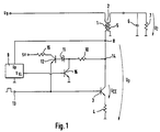
- FIG. 1 shows an ignition device in an internal combustion engine, not shown.
- the primary winding 1 of the ignition coil 2 is connected on the one hand to the supply voltage U B and on the other hand via the collector-emitter path of the ignition transistor 3 and a resistor 4 to ground.
- a load acts on the secondary winding 5 of the ignition coil 2, which is represented here as an equivalent circuit diagram by the parallel connection of a capacitor 6 and a resistor 7.
- a tap 8 is provided between the primary winding 1 and the ignition transistor 3, so that the primary voltage U p is evaluated in an evaluation unit 9, the rise in the primary voltage U p when a trigger pulse is triggered being a measure of the secondary load.
- Another tap 14 between the primary winding and the ignition transistor 3 is connected to the control input of a transistor 12 via a resistor 10 and a zener diode 11.
- the collector of transistor 12 is connected to a 5 volt supply voltage via a resistor 15, while the emitter of transistor 12 is connected to a connection between a control terminal 13 for the ignition signal and the control input of ignition transistor 3.
- a third transistor 16 is connected on the collector side to the connection between the resistor 10 and the Zener diode 11 and is connected to ground on the emitter side. The control input of this third transistor 16 is connected to the evaluation unit 9.
- the ignition system just described has the following mode of operation. Via the control connection 13, the ignition transistor 3 is first controlled to be in the conductive state, so that current flows through the primary winding 1 of the ignition coil 2. At the end of the signal at the control terminal 13, the ignition transistor 3 comes into the non-conductive state, which means an interruption in the current flow in the primary winding 1 of the ignition coil 2 and a high-voltage surge dependent on it in the secondary winding 5 results. This would then lead to an ignition spark on the secondary side of a spark plug, not shown.
- the voltage at the zener diode 11 breaks through and a control current is present at the control input of the transistor 12, so that a control current at the ignition transistor 3 also causes this transistor to react somewhat makes current permeable.
- the voltage across the switching path of the ignition transistor 3 immediately drops again, to the extent that the voltage across the Zener diode 11 falls below the breakdown voltage of this Zener diode.
- the primary voltage U p is detected in the evaluation unit 9 and evaluated in such a way that the voltage building up on the zener diode 11 can be varied by driving the transistor 16, ie the transistor 16 forms an adjustable voltage divider with the resistor 10 , wherein the voltage applied to the center of the adjustable voltage divider corresponds to the voltage applied to the Zener diode 11.
- the voltage potential applied to the zener diode is changed.
- the rise time tr of the primary voltage U p up to a predetermined value is evaluated in the evaluation unit 9. A large capacitive load on the secondary side causes a longer rise time tr than with a small capacitive load.
- the transistor 16 In the case of a long rise time tr, that is to say with a high capacitive load, the transistor 16 is turned on with a correspondingly large voltage and the voltage potential at the zener diode 11 is reduced. In contrast, the transistor 16 is turned on less when the load is low, so that the zener diode 11 reaches the breakdown voltage much earlier than when the capacitive load is high.
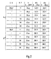
- FIG. 2 shows the relationship between the secondary load and the rise time tr of the primary voltage.
- the table in FIG. 2 is divided into two areas, area a) for larger loads in the secondary circuit and area b) for smaller loads. These areas differ in that two different loads were used for the measurement.
- the table also shows the rise time tr, which corresponds to the time when the primary voltage rose from 0 to 200 V, the voltage change dU 1 (during 25 ⁇ s) and the voltage change dU 2 (during 50 ⁇ s).
- This table in FIG. 2 clearly shows that in the case of the load acting under a (cf. the values for C-6 and R-7), a much longer rise time tr elapses until the primary voltage reaches 200 volts than that for FIG. B specified load. It can be clearly seen that there is a direct connection between the rise time and the secondary load. This relationship is evaluated in the evaluation unit 9 and the transistor 16 is controlled accordingly.
- Another possibility for detecting the secondary load is given by the fact that after a predeterminable time (for example 25 ⁇ s or 50 ⁇ s) the voltage change dU p is recorded by the evaluation unit 9. It can also be seen here from FIG. 2 that the voltage potential in part b) of the table after the same time with a lower load is substantially greater than the voltage potential in part a) of the table.
- Figure 3 shows a possibility of evaluating the detected primary voltage U p .
- the primary voltage U p as already described for FIG. 1, is recorded in a work step 20, wherein, for example, either the rise time tr to 200 V primary voltage U p or the primary voltage U p reached can be evaluated after a predeterminable time.
- the detected primary voltage U p is evaluated as a measure of the attacking secondary load, for example by evaluating the rise time until it reaches 200 V and in step 22 the clamp voltage as described in relation to FIG. 1 is determined by a corresponding control of the transistor 16.
- step 23 the detected primary voltage is compared with reference values U REF of the spark duration and / or the operating voltage curve.
- query 24 it is now checked whether the detected quantities are in the range of the specifiable limit values U REF . If this is the case, the evaluated ignition is recognized as correct in step 25. A no to question 24 leads to work step 26, in which the ignition that has occurred is evaluated as faulty, it being possible at the same time to divide it into different types of fault based on the evaluated operating voltage. A lack of overshoot when the ignition breaks down or a flat rise in voltage indicates shunts on the spark plug. An error display signal is now output in step 27 and the subsequent combustion is evaluated in step 28. Using the evaluation unit 9 in FIG. 1, it is possible, for example, if the increase in the primary voltage and the conclusion on possible shunts is too small, to increase the secondary voltage supply by means of a corresponding brackets U KL in order to cause the spark plug to burn out.
Abstract
Description
Die Erfindung geht aus von einer Zündanlage für Brennkraftmaschinen nach der Gattung des Hauptanspruchs. Es ist schon eine derartige Zündanlage aus der DE-OS 23 39 896 bekannt. Bei dieser bekannten Zündanlage ist im Primärstromkreis zwischen der Primärwicklung und der Schaltstrecke des Zündtransistors eine Verbindung mit einem Element bestimmter Durchbruchs spannung an die Steuerelektrode des Schalttransistors geführt. Übersteigt nun beim Übergang der Schaltstrecke des Zündtransistors in den nicht leitenden Zustand die Spannung den zulässigen Wert, so bricht die Spannung an dem Element bestimmter Durchbruchs spannung durch und es beginnt über die Steuerstrecke des Zündtransistors ein Steuerstrom zu fließen, der die Emitter-Kollektor-Strecke des Zündtransistors wieder etwas stromdurchlässig macht. Dadurch fällt die Spannung an der Schaltstrecke des Zündtransistors wieder ab und zwar soweit, bis die Spannung an dem Schaltelement mit bestimmter Durchbruchs spannung diese Durchbruchsspannung unterschreitet. Diese Anordnung mit dem Element fester Durchbruchsspannung (Zenerdiode) kann nicht für alle Betriebsbereiche den Schutz vor Überspannungen sicherstellen. Legt man beispielsweise die Zündanlage und damit das Elemente mit bestimmter Durchbruchsspannung so aus, daß bei großer Sekundärlast noch ein für alle Betriebszustände ausreichendes Sekundärspannungsangebot zustande kommt, können bei niedriger Sekundärlast höhere Werte an den hochspannungsführenden Teilen auftreten. Eine solche Überlastung kann zu deren Zerstörung führen, wenn z.B. ein Kerzenstecker abfällt und es zum Durchschlag der Hochspannungsisolation kommt.The invention relates to an ignition system for internal combustion engines according to the preamble of the main claim. Such an ignition system is already known from DE-OS 23 39 896. In this known ignition system, a connection with an element of certain breakdown voltage is passed to the control electrode of the switching transistor in the primary circuit between the primary winding and the switching path of the ignition transistor. Now when the switching path of the ignition transistor in the non-conductive state, the voltage exceeds the permissible value, the voltage at the element of certain breakdown voltage breaks through and a control current begins to flow across the control path of the ignition transistor, which the emitter-collector path the ignition transistor makes something current-permeable again. As a result, the voltage across the switching path of the ignition transistor drops again, to the extent that the voltage across the switching element with a certain breakdown voltage falls below this breakdown voltage. This arrangement with the element of fixed breakdown voltage (Zener diode) cannot ensure protection against overvoltages for all operating areas. Lays If, for example, the ignition system and thus the elements with a certain breakdown voltage are made in such a way that a secondary voltage supply sufficient for all operating conditions is achieved with a high secondary load, higher values can occur on the high-voltage parts when the secondary load is low. Such an overload can lead to its destruction if, for example, a plug connector falls off and the high-voltage insulation breaks down.
Bisher bekannte Anlagen arbeiteten mit einer festen Primärzenerung als Spannungsklammerung des Zündtransistors und stellen so einen unzureichenden Kompromiß zwischen ausreichendem Sekundärspannungsangebot und Hochspannungsfestigkeit der hochspannungsführenden Teile dar.Previously known systems worked with a fixed primary generation as voltage clamping of the ignition transistor and thus represent an insufficient compromise between sufficient secondary voltage supply and high-voltage strength of the high-voltage parts.
Die erfindungsgemäße Anordnung mit den kennzeichnenden Merkmalen des Hauptanspruchs hat demgegenüber den Vorteil, daß durch Anpassung der Primärspannungszenerung der Endstufen an die jeweilige sekundäre Last keine zu hohe Spannung am Zündgeschirr bei kleiner Last bzw. kein zu niedriges Spannungsangebot bei hoher Last auftritt.The arrangement according to the invention with the characterizing features of the main claim has the advantage over and above that, by adapting the primary voltage generation of the output stages to the respective secondary load, there is no excessive voltage on the igniter at low load or insufficient voltage supply at high load.
Durch die in den Unteransprüchen aufgeführten Maßnahmen sind vorteilhafte Weiterbildungen und Verbesserungen der im Hauptanspruch angegebenen Zündanlage möglich. Besonders vorteilhaft ist, daß durch Auswertungen der Anstiegszeit der Primärspannung jeweils ein optimaler Spannungswert für einen Zündfunken zur Verfügung steht. Besonders vorteilhaft ist weiterhin, daß als Maß für die sekundäre Last die erreichte Spannung in der Primärwicklung nach Ablauf einer vorgebbaren Zeit auswertbar ist. Somit kann auf veränderte Betriebsbedingungen unmittelbar reagiert werden.Advantageous further developments and improvements of the ignition system specified in the main claim are possible through the measures listed in the subclaims. It is particularly advantageous that, by evaluating the rise time of the primary voltage, an optimum voltage value for an ignition spark is available in each case. It is also particularly advantageous that the voltage reached in the primary winding can be evaluated as a measure of the secondary load after a predefinable time. This means that you can react immediately to changing operating conditions.
Letztendlich bietet das Erfassen der sekundärseitig wirkenden Last den Vorteil, daß Aussagen über das zur Verfügung stehende Zündspannungsangebot möglich sind. So ist beispielsweise die Auswertung der Anstiegszeit der Primärspannung oder das Erreichen eines bestimmten Primär-Spannungswertes innerhalb einer vorgebbaren Zeit als Maß für das Zündspannungsangebot auswertbar. Diese primärseitige Erfassung des Zündspannungsangebots auf der Sekundärseite der Zündspule hat ferner den Vorteil, daß es während des normalen Motorbetriebs zur diagnostischen Auswertung für das Erkennen möglicher Fehler im Zündsystem herangezogen werden kann. So ist ein flacher Anstieg der Sekundärspannung ein Indiz dafür, daß die Zündkerze Nebenschlüsse aufweist. Ist dagegen die erfaßte Funkendauer kürzer als ein Grenzwert bzw. fehlt der für eine Verbrennung typische Brennspannungsverlauf, so fehlt beispielsweise ein zündfähiges Gemisch oder möglicherweise ein Zündfunke an der Zündkerze aufgrund eines abgefallenen Kerzensteckers.Ultimately, the detection of the load acting on the secondary side has the advantage that statements about the available ignition voltage supply are possible. For example, the evaluation of the rise time of the primary voltage or the reaching of a specific primary voltage value within a predeterminable time can be evaluated as a measure of the ignition voltage supply. This primary-side detection of the ignition voltage supply on the secondary side of the ignition coil also has the advantage that it can be used during normal engine operation for diagnostic evaluation to identify possible faults in the ignition system. A flat rise in the secondary voltage is an indication that the spark plug has shunts. If, on the other hand, the detected spark duration is shorter than a limit value or if the burning voltage curve typical for combustion is missing, then for example an ignitable mixture or possibly an ignition spark on the spark plug is missing due to a dropped plug connector.
Das eigentliche Hochspannungsangebot ist z.B. durch Abziehen eines Kerzensteckers und entsprechende Messungen möglich, jedoch ist dies bei Betrieb der Brennkraftmaschine nicht anwendbar. Hier bietet die Auswertung wie oben beschrieben, eine einfache Möglichkeit der Zündspannungserfassung.The actual high voltage offer is e.g. by pulling out a spark plug connector and taking appropriate measurements, but this cannot be used when the internal combustion engine is operating. Here, the evaluation as described above offers a simple way of detecting the ignition voltage.
Ein Ausführungsbeispiel der Erfindung ist in der Zeichnung dargestellt und in der nachfolgenden Beschreibung näher erläutert. Es zeigen Figur 1 den Prinzipaufbau für eine variable Endstufenzenerung, Figur 2 in Tabellenform den Zusammenhang zwischen Sekundärlast und Anstiegsverlauf der Primärspannung und Figur 3 ein Struktogramm zur Erfassung und Auswertung der Primärspannung.An embodiment of the invention is shown in the drawing and explained in more detail in the following description. FIG. 1 shows the basic structure for variable power stage reduction, FIG. 2 shows the relationship between the secondary load and the gradient of the primary voltage in tabular form, and FIG. 3 shows a structure diagram for recording and evaluating the primary voltage.
Figur 1 zeigt eine Zündeinrichtung bei einer nicht dargestellten Brennkraftmaschine. Die Primärwicklung 1 der Zündspule 2 ist einerseits mit der Versorgungsspannung UB und andererseits über die Kollektor-Emitter-Strecke des Zündtransistors 3 und einen Widerstand 4 mit Masse verbunden. An der Sekundärwicklung 5 der Zündspule 2 greift eine Last an, welche hier als Ersatzschaltbild durch die Parallelschaltung eines Kondensators 6 und eines Widerstandes 7 dargestellt ist. Zur Erfassung der Primärspannung ist zwischen der Primärwicklung 1 und dem Zündtransistor 3 ein Abgriff 8 vorgesehen, so daß die Primärspannung Up in einer Auswerteeinheit 9 ausgewertet wird, wobei der Anstiegsverlauf der Primärspannung Up bei Auslösung eines Zündimpulses ein Maß für die sekundäre Last ist. Ein weiterer Abgriff 14 zwischen Primärwicklung und Zündtransistor 3 ist über einen Widerstand 10 und eine Zenerdiode 11 an den Steuereingang eines Transistors 12 geführt. Der Kollektor des Transistors 12 ist über einen Widerstand 15 an eine 5 Volt-Versorgungsspannung geführt, während der Emitter des Transistors 12 an eine Verbindung zwischen einem Steueranschluß 13 für das Zündsignal und dem Steuereingang des Zündtransistors 3 geführt ist. Ein dritter Transistor 16 ist kollektorseitig an die Verbindung zwischen dem Widerstand 10 und der Zenerdiode 11 geführt und emitterseitig gegen Masse geschaltet. Der Steuereingang dieses dritten Transistors 16 ist mit der Auswerteeinheit 9 verbunden.Figure 1 shows an ignition device in an internal combustion engine, not shown. The
Die soeben beschriebene Zündanlage hat folgende Wirkungsweise. Über den Steueranschluß 13 wird der Zündtransistor 3 zunächst in den leitenden Zustand gesteuert, so daß die Primärwicklung 1 der Zündspule 2 von Strom durchflossen wird. Am Ende des Signals an dem Steueranschluß 13 gelangt der Zündtransistor 3 in den nicht leitenden Zustand, was eine Unterbrechung des Stromflusses in der Primärwicklung 1 der Zündspule 2 und einen davon abhängigen Hochspannungsstoß in der Sekundärwicklung 5 zur Folge hat. Dies würde dann sekundärseitig an einer nicht dargestellten Zündkerze zu einem Zündfunken führen. Übersteigt nun beim Übergang des Zündtransistors in den nicht leitenden Zustand die Spannung den zulässigen Wert, so bricht die Spannung an der Zenerdiode 11 durch und an dem Steuereingang des Transistors 12 liegt ein Steuerstrom an, so daß auch ein Steuerstrom am Zündtransistor 3 diesen Transistor wieder etwas stromdurchlässig macht. Dadurch fällt die Spannung an der Schaltstrecke des Zündtransistors 3 sofort wieder ab und zwar soweit, bis die Spannung an der Zenerdiode 11 die Durchbruchs spannung dieser Zenerdiode unterschreitet. Dies ist eine an sich bekannte Spannungsklammerung des Zündtransistors 3, wobei die Primärspannung Up, bei der die Zenerdiode 11 anspricht, als Klammerspannung bezeichnet wird. Am Abgriff 8 wird in der Auswerteeinheit 9 die Primärspannung Up erfaßt und in der Art ausgewertet, daß über eine Ansteuerung des Transistors 16 die sich an der Zenerdiode 11 aufbauende Spannung variert werden kann, d.h. der Transistor 16 bildet mit dem Widerstand 10 einen einstellbaren Spannungsteiler, wobei die an der Mitte des einstellbaren Spannungsteilers anliegende Spannung der Spannung entspricht, die an der Zenerdiode 11 anliegt. Je nach Ansteuerung des Transistors 16 wird das an der Zenerdiode anliegende Spannungspotential verändert. Hierzu wird in der Auswerteeinheit 9 vor allem die Anstiegszeit tr der Primärspannung Up bis zu einem vorgegebenen Wert ausgewertet. So bewirkt eine große kapazitive Last auf der Sekundärseite eine längere Anstiegszeit tr als bei kleiner kapazitiver Last. Bei einer langen Anstiegszeit tr, also bei hoher kapazitiver Last wird der Transistor 16 mit entsprechend großer Spannung aufgesteuert und das angreifende Spannungspotential an der Zenerdiode 11 verkleinert. Im Gegensatz dazu wird bei niedriger Last der Transistor 16 entsprechend weniger aufgesteuert, so daß die Zenerdiode 11 wesentlich früher die Durchbruchsspannung erreicht als bei hoher kapazitiver Last.The ignition system just described has the following mode of operation. Via the
In Figur 2 ist der Zusammenhang zwischen Sekundärlast und Anstiegszeit tr der Primärspannung dargestellt. Die Tabelle in Figur 2 ist in zwei Bereiche, in den Bereich a) für größere Lasten im Sekundärstromkreis und den Bereich b) für kleinere Lasten aufgeteilt. Diese Bereiche unterscheiden sich dadurch, daß bei der Messung jeweils zwei unterschiedliche Lasten verwendet wurden. Weiterhin sind in der Tabelle die Anstiegszeit tr, welche der Zeit des Anstiegs der Primärspannung von 0 auf 200 V entspricht, die Spannungsänderung dU1 (während 25 µs) und die Spannungsänderung dU2 (während 50 µs) dargestellt. Dieser Tabelle in Figur 2 ist deutlich zu entnehmen, daß bei der unter a angreifenden Last (vgl. die Werte bei C-6 und R-7) eine wesentlich größere Anstiegszeit tr bis zum Erreichen von 200 Volt Primärspannung verstreicht als bei der unter Figur b angegebenen Last. Es ist also deutlich zu erkennen, daß ein direkter Zusammenhang zwischen der Anstiegszeit und der Sekundärlast besteht. Dieser Zusammenhang wird in der Auswerteeinheit 9 ausgewertet und der Transistor 16 entsprechend angesteuert.FIG. 2 shows the relationship between the secondary load and the rise time tr of the primary voltage. The table in FIG. 2 is divided into two areas, area a) for larger loads in the secondary circuit and area b) for smaller loads. These areas differ in that two different loads were used for the measurement. The table also shows the rise time tr, which corresponds to the time when the primary voltage rose from 0 to 200 V, the voltage change dU 1 (during 25 µs) and the voltage change dU 2 (during 50 µs). This table in FIG. 2 clearly shows that in the case of the load acting under a (cf. the values for C-6 and R-7), a much longer rise time tr elapses until the primary voltage reaches 200 volts than that for FIG. B specified load. It can be clearly seen that there is a direct connection between the rise time and the secondary load. This relationship is evaluated in the evaluation unit 9 and the transistor 16 is controlled accordingly.
Eine weitere Möglichkeit zur Erfassung der Sekundärlast, ist dadurch gegeben, daß nach einer vorgebbaren Zeit (beispielsweise 25 µs oder 50 µs) von der Auswerteeinheit 9 die Spannungsänderung dUp erfaßt wird. Auch hier ist aus Figur 2 ersichtlich, daß das Spannungspotential im Teil b) der Tabelle nach der gleichen Zeit bei geringerer Last wesentlich größer ist als das Spannungspotential im Teil a) der Tabelle.Another possibility for detecting the secondary load is given by the fact that after a predeterminable time (for example 25 µs or 50 µs) the voltage change dU p is recorded by the evaluation unit 9. It can also be seen here from FIG. 2 that the voltage potential in part b) of the table after the same time with a lower load is substantially greater than the voltage potential in part a) of the table.
Figur 3 zeigt eine Möglichkeit, die erfaßte Primärspannung Up auszuwerten. So wird in einem Arbeitsschritt 20 die Primärspannung Up, wie bereits zu Figur 1 beschrieben, erfaßt, wobei beispielsweise entweder die Anstiegszeit tr bis zum Erreichen 200 V Primärspannung Up oder die erreichte Primärspannung Up nach einer vorgebbaren Zeit auswertbar ist. Im anschließenden Arbeitsschritt 21 wird die erfaßte Primärspannung Up als Maß für die angreifende Sekundärlast, indem z.B. die Anstiegszeit bis zum Erreichen 200 V bewertet wird ausgewertet und im Arbeitsschritt 22 die Klammerspannung wie zu Figur 1 beschrieben, über eine entsprechende Ansteuerung des Transistors 16 festgelegt.Figure 3 shows a possibility of evaluating the detected primary voltage U p . The primary voltage U p , as already described for FIG. 1, is recorded in a
Im Arbeitsschritt 23 wird die erfaßte Primärspannung mit Referenzwerten UREF der Funkendauer und/oder des Brennspannungsverlaufs verglichen. In der Abfrage 24 wird nun geprüft, ob die erfaßten Größen im Bereich der vorgebbaren Grenzwerte UREF liegen. Ist dies der Fall, so wird im Arbeitsschritt 25 die ausgewertete Zündung als ordnungsgemäß erkannt. Ein Nein auf die Frage 24 führt zum Arbeitsschritt 26, in welchem die erfolgte Zündung als fehlerhaft gewertet wird, wobei gleichzeitig eine Einteilung in verschiedene Fehlerarten aufgrund der ausgewerteten Brennspannung möglich ist. So läßt ein fehlendes Überschwingen beim Durchbruch der Zündung bzw. ein flacher Spannungsanstieg auf Nebenschlüsse an der Zündkerze schließen. Im Arbeitsschritt 27 wird nun ein Fehleranzeige-Sginal ausgegeben und im Arbeitsschritt 28 die darauffolgende Verbrennung ausgewertet. Über die Auswerteeinheit 9 der Figur 1 ist es möglich, beispielsweise bei einem zu geringen Anstieg der Primärspannung und der Schlußfolgerung auf mögliche Nebenschlüsse das Sekundärspannungsangebot über eine entsprechende Klammerung UKL zu erhöhen, um so ein Freibrennen der Zündkerze zu bewirken.In
Claims (6)
- Ignition system for internal combustion engines, with an ignition coil and an ignition output stage (3) in series with the primary winding (1) of the ignition coil, with a terminal circuit (10,11,12,16) which limits the primary current flowing in the primary winding of the ignition coil when a prescribable primary voltage at the connection (14) between the primary winding (1) and ignition output stage (3) is exceeded, and contains at least one switching element (11) with a specific breakdown voltage, the branch of the terminal circuit (10,11, 12,16) which contains the switching element (11) with a specific breakdown voltage being led from the connection (14) between the primary winding (1) and ignition output stage (3) to the control electrode of the ignition output stage (3), characterized in that the terminal circuit (10,11,12,16) can be modified with an evaluation unit (9), connected between the primary winding (1) and ignition output stage (3), as a function of a secondary-side load (6,7), in such a way that the terminal circuit (10,11,12,16) limits the primary voltage in the case of a high secondary load with a high primary voltage and in the case of a low secondary load with a correspondingly low primary voltage.
- Ignition system according to Claim 1, characterized in that the evaluation unit (9) detects the rise time (tr) of the primary voltage (Up) as a measure of the secondary load.
- Ignition system according to Claim 2, characterized in that the evaluation unit (9) detects the time between the ignition time and the time when a prescribable threshold voltage is reached in the primary winding as a measure of the rise time (tr).
- Ignition system according to Claim 1, characterized in that, after a prescribable time after the ignition time, the evaluation unit (9) detects the voltage in the primary winding as a measure of the secondary load.
- Ignition system according to one of the preceding claims, characterized in that the detected primary voltage (Up) can be compared with limit values (UREF) for spark length and/or sparking voltage profile which represent a correct combustion.
- Ignition system according to Claim 5, characterized in that, in the case of a deviation of the primary voltage from the limit values, a faulty combustion is detected and a fault display signal (27) is output.
Applications Claiming Priority (5)
| Application Number | Priority Date | Filing Date | Title |
|---|---|---|---|
| DE4233211 | 1992-10-02 | ||
| DE4233211 | 1992-10-02 | ||
| DE4315999A DE4315999A1 (en) | 1992-10-02 | 1993-05-13 | Ignition system for internal combustion engines |
| DE4315999 | 1993-05-13 | ||
| PCT/DE1993/000817 WO1994008133A1 (en) | 1992-10-02 | 1993-09-08 | Ignition system with variable primary voltage limitation and defect diagnosis |
Publications (2)
| Publication Number | Publication Date |
|---|---|
| EP0615580A1 EP0615580A1 (en) | 1994-09-21 |
| EP0615580B1 true EP0615580B1 (en) | 1997-05-28 |
Family
ID=25919137
Family Applications (1)
| Application Number | Title | Priority Date | Filing Date |
|---|---|---|---|
| EP93918954A Expired - Lifetime EP0615580B1 (en) | 1992-10-02 | 1993-09-08 | Ignition system with variable primary voltage limitation and defect diagnosis |
Country Status (5)
| Country | Link |
|---|---|
| EP (1) | EP0615580B1 (en) |
| JP (1) | JP3402608B2 (en) |
| DE (2) | DE4315999A1 (en) |
| ES (1) | ES2102671T3 (en) |
| WO (1) | WO1994008133A1 (en) |
Family Cites Families (6)
| Publication number | Priority date | Publication date | Assignee | Title |
|---|---|---|---|---|
| US3749974A (en) * | 1971-06-01 | 1973-07-31 | Chrysler Corp | Electronic ignition controller |
| JPS5819850B2 (en) * | 1977-09-30 | 1983-04-20 | 株式会社日立製作所 | Non-contact ignition device for internal combustion engine |
| DE2811149A1 (en) * | 1978-03-15 | 1979-09-20 | Bosch Gmbh Robert | ELECTRICAL CIRCUIT WITH A SWITCHING TRANSISTOR AND WITH AN INDUCTIVE RESISTOR, IN PARTICULAR WITH THE PRIMARY DEVELOPMENT OF AN IGNITION COIL TO A COMBUSTION MACHINE |
| DE3019162C2 (en) * | 1980-05-20 | 1985-11-07 | Telefunken electronic GmbH, 7100 Heilbronn | Transistor ignition circuit |
| JPS60147571A (en) * | 1984-01-12 | 1985-08-03 | Toshiba Corp | Ignition device |
| US4913123A (en) * | 1989-03-23 | 1990-04-03 | Ford Motor Company | Ignition timing system with feedback correction |
-
1993
- 1993-05-13 DE DE4315999A patent/DE4315999A1/en not_active Withdrawn
- 1993-09-08 DE DE59306600T patent/DE59306600D1/en not_active Expired - Fee Related
- 1993-09-08 WO PCT/DE1993/000817 patent/WO1994008133A1/en active IP Right Grant
- 1993-09-08 JP JP50856894A patent/JP3402608B2/en not_active Expired - Fee Related
- 1993-09-08 ES ES93918954T patent/ES2102671T3/en not_active Expired - Lifetime
- 1993-09-08 EP EP93918954A patent/EP0615580B1/en not_active Expired - Lifetime
Also Published As
| Publication number | Publication date |
|---|---|
| JP3402608B2 (en) | 2003-05-06 |
| ES2102671T3 (en) | 1997-08-01 |
| EP0615580A1 (en) | 1994-09-21 |
| DE4315999A1 (en) | 1994-04-07 |
| JPH07501599A (en) | 1995-02-16 |
| WO1994008133A1 (en) | 1994-04-14 |
| DE59306600D1 (en) | 1997-07-03 |
Similar Documents
| Publication | Publication Date | Title |
|---|---|---|
| DE19502402C2 (en) | Misfire sampling circuit for an internal combustion engine | |
| EP0790406B1 (en) | Electronic ignition system for internal combustion engines | |
| DE102015203758B4 (en) | Internal combustion engine control device | |
| DE10012854B4 (en) | Combustion state detection device for an internal combustion engine | |
| DE19500452B4 (en) | Method and device for monitoring the functionality of an idle actuator | |
| DE19733869A1 (en) | Device for determining the combustion state of an internal combustion engine | |
| DE4133015C2 (en) | Ignition system for multi-cylinder internal combustion engines | |
| EP0389775B1 (en) | Watch circuit of the high voltage in an ignition device | |
| DE69936426T2 (en) | Sensor for determining the ignition current and the ion current in the ignition secondary circuit | |
| EP0848161B1 (en) | Inductive ignition coils system for motor | |
| DE4239803C2 (en) | Ionization current detector device for an internal combustion engine | |
| DE4020986C2 (en) | Electronic ignition system for an internal combustion engine | |
| DE19926079A1 (en) | Arrangement for detecting internal combustion engine combustion state has discharge current limiter between ignition current path formed by ion discharge at ignition plug, bias device | |
| DE4305197C2 (en) | Ignition device for a multi-cylinder engine | |
| DE2823788C2 (en) | ||
| EP0615580B1 (en) | Ignition system with variable primary voltage limitation and defect diagnosis | |
| DE2701896C3 (en) | Electrical circuit troubleshooting device | |
| DE4142666C2 (en) | Circuit arrangement with a semiconductor switch for switching a load | |
| EP0502549B1 (en) | Spark survey in spark ignition engine | |
| DE3417676C2 (en) | ||
| DE3806649C2 (en) | ||
| DE3823963C2 (en) | Circuit arrangement for generating a constant supply voltage | |
| DE69813475T2 (en) | Ionization sensor in the ignition system of an internal combustion engine | |
| DE2821085A1 (en) | Ignition system for IC engine - has Zener diodes in circuit parallel to transistor, preventing overvoltages on both sides of ignition coil | |
| DE2940036C2 (en) |
Legal Events
| Date | Code | Title | Description |
|---|---|---|---|
| PUAI | Public reference made under article 153(3) epc to a published international application that has entered the european phase |
Free format text: ORIGINAL CODE: 0009012 |
|
| 17P | Request for examination filed |
Effective date: 19940513 |
|
| AK | Designated contracting states |
Kind code of ref document: A1 Designated state(s): DE ES FR |
|
| 17Q | First examination report despatched |
Effective date: 19960416 |
|
| GRAG | Despatch of communication of intention to grant |
Free format text: ORIGINAL CODE: EPIDOS AGRA |
|
| GRAH | Despatch of communication of intention to grant a patent |
Free format text: ORIGINAL CODE: EPIDOS IGRA |
|
| GRAH | Despatch of communication of intention to grant a patent |
Free format text: ORIGINAL CODE: EPIDOS IGRA |
|
| GRAA | (expected) grant |
Free format text: ORIGINAL CODE: 0009210 |
|
| AK | Designated contracting states |
Kind code of ref document: B1 Designated state(s): DE ES FR |
|
| ET | Fr: translation filed | ||
| REF | Corresponds to: |
Ref document number: 59306600 Country of ref document: DE Date of ref document: 19970703 |
|
| REG | Reference to a national code |
Ref country code: ES Ref legal event code: FG2A Ref document number: 2102671 Country of ref document: ES Kind code of ref document: T3 |
|
| PLBE | No opposition filed within time limit |
Free format text: ORIGINAL CODE: 0009261 |
|
| STAA | Information on the status of an ep patent application or granted ep patent |
Free format text: STATUS: NO OPPOSITION FILED WITHIN TIME LIMIT |
|
| 26N | No opposition filed | ||
| PGFP | Annual fee paid to national office [announced via postgrant information from national office to epo] |
Ref country code: FR Payment date: 20030819 Year of fee payment: 11 |
|
| PGFP | Annual fee paid to national office [announced via postgrant information from national office to epo] |
Ref country code: ES Payment date: 20030826 Year of fee payment: 11 |
|
| PGFP | Annual fee paid to national office [announced via postgrant information from national office to epo] |
Ref country code: DE Payment date: 20031029 Year of fee payment: 11 |
|
| PG25 | Lapsed in a contracting state [announced via postgrant information from national office to epo] |
Ref country code: ES Free format text: LAPSE BECAUSE OF NON-PAYMENT OF DUE FEES Effective date: 20040909 |
|
| PG25 | Lapsed in a contracting state [announced via postgrant information from national office to epo] |
Ref country code: DE Free format text: LAPSE BECAUSE OF NON-PAYMENT OF DUE FEES Effective date: 20050401 |
|
| PG25 | Lapsed in a contracting state [announced via postgrant information from national office to epo] |
Ref country code: FR Free format text: LAPSE BECAUSE OF NON-PAYMENT OF DUE FEES Effective date: 20050531 |
|
| REG | Reference to a national code |
Ref country code: FR Ref legal event code: ST |
|
| REG | Reference to a national code |
Ref country code: ES Ref legal event code: FD2A Effective date: 20040909 |