EP0613272B1 - Resynchronization of asynchronous transfer mode (ATM) switch fabric - Google Patents
Resynchronization of asynchronous transfer mode (ATM) switch fabric Download PDFInfo
- Publication number
- EP0613272B1 EP0613272B1 EP93309769A EP93309769A EP0613272B1 EP 0613272 B1 EP0613272 B1 EP 0613272B1 EP 93309769 A EP93309769 A EP 93309769A EP 93309769 A EP93309769 A EP 93309769A EP 0613272 B1 EP0613272 B1 EP 0613272B1
- Authority
- EP
- European Patent Office
- Prior art keywords
- memory unit
- queues
- individual ones
- switch
- cells
- Prior art date
- Legal status (The legal status is an assumption and is not a legal conclusion. Google has not performed a legal analysis and makes no representation as to the accuracy of the status listed.)
- Expired - Lifetime
Links
Images



Classifications
-
- H—ELECTRICITY
- H04—ELECTRIC COMMUNICATION TECHNIQUE
- H04L—TRANSMISSION OF DIGITAL INFORMATION, e.g. TELEGRAPHIC COMMUNICATION
- H04L12/00—Data switching networks
- H04L12/54—Store-and-forward switching systems
- H04L12/56—Packet switching systems
- H04L12/5601—Transfer mode dependent, e.g. ATM
-
- H—ELECTRICITY
- H04—ELECTRIC COMMUNICATION TECHNIQUE
- H04L—TRANSMISSION OF DIGITAL INFORMATION, e.g. TELEGRAPHIC COMMUNICATION
- H04L49/00—Packet switching elements
- H04L49/10—Packet switching elements characterised by the switching fabric construction
- H04L49/104—Asynchronous transfer mode [ATM] switching fabrics
- H04L49/105—ATM switching elements
- H04L49/106—ATM switching elements using space switching, e.g. crossbar or matrix
-
- H—ELECTRICITY
- H04—ELECTRIC COMMUNICATION TECHNIQUE
- H04L—TRANSMISSION OF DIGITAL INFORMATION, e.g. TELEGRAPHIC COMMUNICATION
- H04L49/00—Packet switching elements
- H04L49/15—Interconnection of switching modules
- H04L49/1553—Interconnection of ATM switching modules, e.g. ATM switching fabrics
-
- H—ELECTRICITY
- H04—ELECTRIC COMMUNICATION TECHNIQUE
- H04L—TRANSMISSION OF DIGITAL INFORMATION, e.g. TELEGRAPHIC COMMUNICATION
- H04L49/00—Packet switching elements
- H04L49/25—Routing or path finding in a switch fabric
- H04L49/253—Routing or path finding in a switch fabric using establishment or release of connections between ports
- H04L49/255—Control mechanisms for ATM switching fabrics
-
- H—ELECTRICITY
- H04—ELECTRIC COMMUNICATION TECHNIQUE
- H04Q—SELECTING
- H04Q11/00—Selecting arrangements for multiplex systems
- H04Q11/04—Selecting arrangements for multiplex systems for time-division multiplexing
- H04Q11/0428—Integrated services digital network, i.e. systems for transmission of different types of digitised signals, e.g. speech, data, telecentral, television signals
- H04Q11/0478—Provisions for broadband connections
-
- H—ELECTRICITY
- H04—ELECTRIC COMMUNICATION TECHNIQUE
- H04L—TRANSMISSION OF DIGITAL INFORMATION, e.g. TELEGRAPHIC COMMUNICATION
- H04L12/00—Data switching networks
- H04L12/54—Store-and-forward switching systems
- H04L12/56—Packet switching systems
- H04L12/5601—Transfer mode dependent, e.g. ATM
- H04L2012/5625—Operations, administration and maintenance [OAM]
- H04L2012/5627—Fault tolerance and recovery
-
- H—ELECTRICITY
- H04—ELECTRIC COMMUNICATION TECHNIQUE
- H04L—TRANSMISSION OF DIGITAL INFORMATION, e.g. TELEGRAPHIC COMMUNICATION
- H04L12/00—Data switching networks
- H04L12/54—Store-and-forward switching systems
- H04L12/56—Packet switching systems
- H04L12/5601—Transfer mode dependent, e.g. ATM
- H04L2012/5678—Traffic aspects, e.g. arbitration, load balancing, smoothing, buffer management
- H04L2012/5681—Buffer or queue management
Definitions
- This invention relates to switch arrangements.
- duplicated buffer memory units are employed in an active-standby configuration to reduce so-called "down time" in the presence of a failure and, thereby improve system reliability.
- proper system operation requires that the contents of each of the memory units be identical.
- Prior arrangements are known (see e.g. EP-A-0 410139) in which synchronization of such duplicated memory units is realized.
- ATM transmission of data is on a cell-by-cell basis wherein each cell comprises a fixed length packet.
- the terms cell and packet are interchangeable.
- a plurality of queues is employed to store cells, with each of the queues being associated on a one-to-one basis with either inputs or outputs of the memory unit.
- Synchronization of the active and standby memory units is realized in this prior arrangement by employing a queue length counter with each queue and observing when all of the counters have reached zero count at least once.
- the lengths of data in corresponding queues i.e., the number of cells stored in the corresponding queues, in the active and standby memory units are compared on a cell-interval-by-cell-interval basis. If the number of cells stored in any of the queues is different than the number of cells in its corresponding queue in the other of the memory units during any cell interval, resynchronization of the memory units is initiated.
- the outputs of corresponding queues in the active memory unit and the standby memory unit are compared on a cell-interval-by-cell-interval basis. If the results of the comparison indicates that any one or more of the queue outputs in one of the memory units is different from the output of the corresponding queue in the other memory unit, resynchronization is initiated.
- robustness of the resynchronization initiation is further enhanced by simultaneously employing both the comparison of cell length in the queues and the comparison of the queue output contents to detect when to initiate resynchronization.
- FIG. 1 shows, in simplified bock diagram form, an exemplary duplicated NxN switch arrangement 100, including an embodiment of the invention.
- Switch 100 is particularly suited for use in Asynchronous Transfer Mode (ATM) switching and/or transmission systems.
- ATM Asynchronous Transfer Mode
- Such a system may constitute either a stand-alone switch 100 or a portion of a switch made up of a plurality of such switches 100.
- Switch 100 includes a duplicate pair of NxN switch modules 101 and 102 which are arranged to operate in active-standby modes for fault-tolerance purposes.
- Switch modules 101 and 102 include buffer memory and control units 126 and 127, respectively. Each of buffer memory and control units 126 and 127 includes a plurality of N queues (not shown) which are controlled by a controller (not shown) for storing incoming cells from the plurality of inputs 112-1 through 112-N and controllably supplying them to outputs 114-1 through 114-N. Such buffer memory and control units are well known in the art.
- Switch modules 101 and 102 also include queue (Q)-length comparators 103 and 104, respectively.
- Q-length comparator 103 includes queue (Q)-empty comparator 105 and queue (Q)-empty indicator 106.
- Q-length comparator 104 includes Q-empty comparator 107 and Q-empty indicator 108.
- Received digital signals are supplied via inputs 110-1 through 110-N and receive line interfaces 111-1 through 111-N to inputs 112-1 through 112-N, respectively, of switch modules 101 and 102.
- Each of receive line interface units 111 perform functions such as clock recovery, framing and other well known functions commonly associated with digital receive line interface units.
- receive line interface units 111 also perform functions such as ATM cell delineation and the like which are also well known for such ATM systems.
- the received ATM cell stream contains a continuous stream of ATM cells which, in general include idle cells and non-idle cells.
- the incoming ATM line rate is 155.52 Mb/s, which is known as the STM-1 rate, although the invention is not limited in this regard.
- the ATM cell stream is typically accompanied by a BIT/WORD Clock which, depending on the particular implementation may be a clock at the bit rate of the ATM cell stream if the implementation is a serial one or, more typically, a sub-multiple of the ATM cell stream bit rate if data are carried on a parallel bus.
- a Cell Clock is present, which provides information that identifies the boundaries of the fixed length cells. Those skilled in the art will know how to employ such clocks in an ATM system employing the invention.
- the outputs of receive line interface units 111-1 through 111-N are dual fed to inputs 112-1 through 112-N of each of switch modules 101 and 102 and, therein, to the N queues in buffer memory and control units 126 and 127, respectively.
- Switch modules 101 and 102 which are also referred to as side 0 and side 1 switch modules, respectively, are redundant with each other, i.e., their internal states and all of their N queues should be the same. That is to say, cell contents of the N queues in each of buffer memory and control units 126 and 127 of switch modules 101 and 102 respectively, should be identical.
- switch modules 101 and 102 operate on all N inputs simultaneously to provide N outputs, namely, outputs 114-1 through 114-N from switch module 101, and outputs 115-1 through 115-N from switch module 102. These outputs are supplied in pairs to transmit line interface units 116-1 through 116-N.
- output 114-1 from switch module 101 and output 115-1 from switch module 102 are supplied to transmit line interface 116-1 while output 114-N from switch module 101 and output 115-N from switch module 102 are supplied to transmit line interface 116-N. Only transmit line interface 116-1 will be described in detail, all other of the transmit line interface units 116 being identical in structure and operation.
- output 114-1 from switch module 101 and output 115-1 from switch module 102 are supplied to cell selector and comparator 117 of transmit line interface 116-1 and, therein, to inputs of 2:1 selector 119 and cell comparator and idle cell detector 120.
- the 2:1 selector 119 is responsive to a select control signal (SEL) from processor 123 to select output 114-1 or 115-1 according to whether side 0 switch module 101 or side 1 switch module 102, respectively, has been designated as the active switch module.
- SEL select control signal
- the output from 2:1 selector 119 is further processed via line interface 118 prior to transmission on output 122-1.
- Line interface 118 performs further processing related to formatting and timing of the digital signal for transmission in well-known fashion.
- Outputs from cell comparator and idle cell detector 120 are processed by cell comparator state machine (CCSM) 121 to determine whether or not there is an out-of-sync comparison. If so, an out-of-sync signal OSC-1 is supplied to processor 123. A reset signal is supplied from processor 123 as required to reset CCSM 121 to its in-sync condition.
- CCSM cell comparator state machine
- Q-length comparator 103 includes the combination of Q-empty comparator 105 and Q-empty indicator 106
- Q-length comparator 104 includes the combination of Q-empty comparator 107 and Q-empty indicator 108. Since the apparatus and operation of Q-length comparators 103 and 104 are identical only the operation of Q-length comparator 103 in side 0 switch module 101 will be described.
- Q-empty indicator 106 generates N binary Q-empty indicator signals, each of which indicates whether or not a corresponding one of the N queues in the buffer memory in switch module 101 is empty.
- each Q-empty indicator signal indicates whether or not the corresponding queue has cells therein pending transmission as an output.
- the N Q-empty indicator signals are supplied via N lines 124 to Q-empty comparator 105 in switch module 101 and to Q-empty comparator 107 in switch module 102.
- the N Q-empty indicator signals from Q-empty indicator 108 in switch module 102 are supplied via N lines 125 to Q-empty comparator 107 and to Q-empty comparator 105 in switch module 101.
- These Q-empty indicator signals are readily obtained from known queue-control circuitry (not shown) that manages the queues within each of buffer memory and control units 126 and 127 of switch modules 101 and 102, respectively.
- a queue length counter to determine when a corresponding queue is empty, i.e., when a count of zero (0) cells is obtained.
- the N Q-empty indicator signals supplied to Q-empty comparator 105 from Q-empty indicator 106 and Q-empty indicator 108 are compared on a pair-wise basis. At each cell interval, Q-empty comparator 105 performs an N-wise comparison of the pairs of N Q-empty indicator signals. An inequality of any one or more in the N pairs of Q-empty indicator signals, indicates that switch module 101 and switch module 102 are out-of-synchronization and this indication is provided by an out-of-synchronization (OSQ (0)) signal from Q-empty comparator 105.
- OSQ (1) signal would be supplied from Q-empty comparator 107.
- FIG. 2 shows one possible implementation of Q-empty comparators 105 and 107 of FIG. 1.
- the Q-empty comparator includes comparator blocks 201-1 through 201-N, one for each pair of Q-empty indicators 124-1, 125-1 through 124-N, 125-N, respectively. An output is supplied from each of comparator blocks 201-1 through 201-N to NOR-gate 205. Since the apparatus and operation of comparator blocks 201-1 through 201-N are identical, only comparator 201-1 will be described in detail. It is noted that either Q-empty indicator 124-1 or 125-1 is active in this example when it is a logical 1 which indicates that corresponding queue is empty. Q-empty indicators 124-1 and 125-1 are supplied to exclusive OR-gate 202-1.
- Exclusive OR-gate 202-1 generates at its output a logical 1 signal when Q-empty indicators 124-1 and 125-1 are not equal.
- flip-flop 203-1 latches the state of the output of exclusive OR-gate 202-1.
- Cell clock 204 may be derived in any number of known ways.
- Flip-flop 203-1 is a D-type flip-flop which operates as follows: if its enable (E) input is active (logic 1), when it is clocked by cell clock, then the input to data (D) input appears at the output (Q); otherwise, the output (Q) remains unchanged; if the reset input (R) is active (logic 0), the output (Q) is set to logic 0 regardless of the states of the (D) and (E) inputs.
- NOR-gate 205 combines the N output indications from comparator stages 201-1 through 201-N. The output of the combination from NOR-gate 205 is supplied to latch 206 which is set to an active state if any of the N pairs of Q-empty indicator signals 124, 125 indicates a mismatch at any cell time. Latch 206 supplies an active (logic 1) output OSQ to processor 123 until it is reset in response to an active reset signal from processor 123.
- each queue must periodically be empty.
- an inequality in the length of corresponding queues will manifest itself when the queue having the shorter length, i.e., lower number of cells therein, is emptied and the queue having the longer length, i.e., larger number of cells therein, has one or more cells remaining; at that instant, Q-empty comparator 105 will detect the inequality.
- cell comparator and idle cell detector 120 Another apparatus and technique for detecting when to initiate resynchronization is realized by the combination of cell comparator and idle cell detector 120 and cell comparator state machine (CCSM) 121 in each of transmit line interface units 116-1 through 116-N.
- cell comparator and idle cell detector 120 compares the contents of the cell on output 114-1 from switch module 101 to the contents of the cell on output 115-1 from switch module 102. If any bit in these cells indicates a difference in the contents of the cell, cell comparator and idle cell detector 120 supplies an output indicating this state to CCSM 121.
- the output from cell comparator and idle cell detector 120 could indicate one of four comparison states, viz, whether the cells were equal and idle, whether the cells were equal and non-idle, whether the cells differed in one (1) bit position or whether the cells differed in more than one (1) bit position.
- idle cell detection is realized in a known fashion by comparing the received cell header to an expected idle cell pattern.
- an idle cell has a distinct header as defined in CCITT Recommendation I.361 entitled "B-ISDN ATM Layer Specification".
- CCSM 121 processes the supplied indication in a predefined manner, e.g., CCSM 121 could wait for a few consecutive multiple-bit mismatches between the cells prior to indicating an out-of -synchronization state, since a single-bit mismatch may be indicative of only a random bit error.
- CCSM 121 supplies an out-of-sync indication signal OSC-1 to processor 123.
- CCSM 121 could wait for several consecutive matches of cells prior to indicating a return to the in-synchronization state.
- the performance of CCSM 121 can be improved considerably by having it ignore the occurrence of idle cells on both inputs to comparator and idle cell detector 120. This is important because under low traffic conditions, the number of idle cells may be so large that they could otherwise falsely indicate an in-synchronization state.
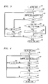
- FIG. 3 shows a flow chart illustrating one example of the operation of CCSM 121 when in an in-synchronization state and going to an out-of-synchronization state.
- Step 303 compares the bits in the cells from modules 101 and 102.
- Step 304 determines whether or not the cells are equal. If the test result in step 304 is yes, step 305 tests to determine whether or not the cells are idle cells. This determination is readily obtained in known fashion from the contents of the cell. If the test result is yes, control is returned to step 303.
- step 309 If the test result in step 309 is yes, P consecutive mismatches have been detected and an out-of-synchronization state is declared via step 310 and the OSC-1 signal is supplied to processor 123 (FIG. 1).
- the parameter P may be selected based on the performance requirements and characteristics of the system, but would generally be a small value, on the order of one (1) or two (2) cells. It is noted that those skilled in the art may employ alternative algorithms for determining the out-of sync condition without deviating from the invention.
- FIG. 4 is a flow chart illustrating the operation of CCSM 121 when in an out-of-sync state and going towards an in-sync state.
- the process is entered via step 310, i.e., out-of-sync.
- the parameter Q may also be selected based on the performance requirements and characteristics of the particular system, but would generally be on the order of several cells and greater than the parameter P.
- Out-of-sync indicators OSQ (0) from switch module 101, OSQ (1) from switch module 102 and out-of-sync indicators OSC-1 through OSC-N from transmit line interfaces 116-1 through 116-N are supplied to processor 123 of FIG. 1. It is noted that all of these out-of-synchronization indicator signals are latched and, therefore, there is no need for processor 123 to respond within any one cell interval. Any one of the out-of-synchronization indicator signals being active indicates that switch modules 101 and 102 are out-of-synchronization, but processor 123 may implement any one of a number of approaches to making an out-of-synchronization determination.
- processor 123 may first reset Q-empty comparators 105 and 107 in switch modules 101 and 102, respectively, and each CCSM 121 in transmit line interfaces 116-1 through 116-N and verify that an out-of-synchronization condition reappears. Once processor 123 has verified that switch modules 101 and 102 are out-of-synchronization, it will initiate procedures to resynchronize them.
- processor 123 may first reset Q-empty comparators 105 and 107 in switch modules 101 and 102, respectively, and each CCSM 121 in transmit line interfaces 116-1 through 116-N and verify that an out-of-synchronization condition reappears. Once processor 123 has verified that switch modules 101 and 102 are out-of-synchronization, it will initiate procedures to resynchronize them.
- One example of a synchronization technique which may advantageously be employed is described in U.S. Patent application Serial 07/739,928, cited above. The particular procedure used in processor 123 could depend on which one or more out-of-synchronization indicator signals have been activated.
- processor 123 activates the reset signal to reset Q-empty comparators 105 and 107 and all of the CCSMs 121 in transmit line interfaces 116-1 through 116-N and is then ready to detect the next occurrence of an out-of- synchronization condition to initiate resynchronization of switch modules 101 and 102.
- multi-stage switches are assumed to have the following additional characteristics that the single stage switch 100 of FIG. 1 does not: they may be comprised of two or more cascaded or networked switch stages comprising duplicated switch modules, each of the switch modules has a set of queues associated with it and each such switch stage may be cross-coupled to a previous switch stage so that they are in so-called "separate protection groups", i.e., the side 0 switch module of stage 2 switch will receive inputs from both side 0 and side 1 switch modules of stage 1 and will select one of the two.
- FIG. 5 shows, in simplied block diagram form, one embodiment of a multi-stage switch 500, including the invention.
- a first stage of the switch 500 includes NxN switch modules 101 and 102 including Q-length comparators 103 and 104, respectively, which are identical in structure and operation to those described above in relationship to FIG. 1.
- a second stage of the switch 500 comprises output stages 501-1 through 501-N which are identical. Only output stage 501-1 will be described in detail.
- output stage 501-1 includes a side 0 demultiplexer (DEMUX) stage 502 and a side 1 demultiplexer (DEMUX) stage 503.
- Stage 502 includes cell selector and comparator 117(0), side 0 DEMUX 504 and Q-length comparator 103-1.
- demultiplexer stage 503 includes cell selector and comparator 117(1), side 1 DEMUX 505 and Q-length comparator 104-1.
- Cell selector and comparator 117 (0) and cell selector and comparator 117 (1) are identical in structure and operation to cell selector and comparator 117, shown in FIG. 1 and described above.
- both cell selector and comparator 117 (0) and 117 (1) are supplied with outputs 114-1 from side 0 switch module 101 and 115-1 from side 1 switch module 102.
- Cell selector and comparator 117 (0) is responsive to a SEL 1 control signal from processor 510 to select either the signal on output 114-1 or the signal on output 115-1 to DEMUX 504.
- DEMUX 504 is operative to demultiplex the signal supplied thereto from cell selector and comparator 117 (0) into M individual signals each having a rate which is 1/M of the signal supplied as an input thereto. These M signals are, in turn, supplied via outputs 511-1 through 511-M to cell selector and comparators 117-1 through 117-M.
- DEMUX 504 includes a plurality of M queues and the associated queue control circuitry (not shown).
- Q-length comparator 103-1 interacts with the M queues and associated Q control circuitry in DEMUX 504 to compare the lengths of the queues in DEMUX 504 and DEMUX 505.
- the structure and operation of Q-length comparator 103-1 is analogous to Q-length comparator 103 of FIG. 1 and described above. The only differences being that the number of queues being compared is M and they are operating at a bit rate which is 1/M of the bit rate of the signal being suppled to DEMUX 504. To this end, M Q-empty indications are supplied via M-lines 508 from Q-length comparator 103-1 to Q-length comparator 104-1 and vice-versa via M-lines 509.
- Q-length comparator 103-1 is operative to generate out-of-synchronization indicator signal OSQ-1 (0) which is supplied to processor 510.
- cell selector and comparator 117 (1) is responsive to a SEL 1 control signal from processor 510 to select either the signal on output 114-1 or the signal on output 115-1 to DEMUX 505. It is also operative to generate the out-of-synchronization indication signal OSC-1 (1) in the same manner as cell selector and comparator 117 of FIG. 1, described above.
- Side 1 DEMUX 505 is operative to demultiplex the signal supplied thereto from cell selector and comparator 117 (1) into M individual signals each having a rate which is 1/M of the signal supplied as an input thereto.
- DEMUX 505 includes a plurality of M queues and the associated queue control circuitry (not shown).
- Q-length comparator 104-1 interacts with the M queues and associated Q control circuitry in DEMUX 505 to compare the lengths of the queues in DEMUX 504 and DEMUX 505.
- the structure and operation Q-length comparator 104-1 is analogous to Q-length comparator 104 of FIG. 1 and described above. The only differences being that the number of queues being compared is M and they are operating at a bit rate which is 1/M of the bit rate of the signal being suppled to DEMUX 505.
- M Q-empty indications are supplied via M-lines 509 from Q-length comparator 104-1 to Q-length comparator 103-1 and vice-versa via M-lines 508, as indicated above.
- Q-length comparator 104-1 is operative to generate out-of-synchronization indicator signal OSQ-1 (1) which is supplied to processor 510.
- Each of cell selector and comparators 117-1 through 117-M is operative to select the corresponding output from either DEMUX 504 or DEMUX 505 to be supplied to line interface units 506-1 through 506-M, respectively.
- line interface units 506-1 through 506-M supply the selected signal to output lines 507-1 through 507-M.
- cell selector and comparators 117-1 through 117-M are responsive to a SEL 2 control signal supplied from processor 510 to select as an output either the signal supplied from side 0 DEMUX 504 or side 1 DEMUX 505 as an output to line interface units 506-1 through 506-M, respectively.
- cell selector and comparators 117-1 through 117-M are operative to generate out-of-synchronization indication signals OSC-1-1 through OSC-1-M.
- cell selector and comparators 117-1 through 117-M are identical in structure and operation to cell selector and comparator 117 of FIG. 1 and described above, except they are operating at a bit rate which is 1/M of the bit rate of the signal being supplies as an input to output stage 501-1.
- Processor 510 is responsive to the out-of-sync indication signals, namely OSQ (0), OSQ (1), OSQ-1 (0) through OSQ-N (0), OSQ-1 (1) through OSQ-N (1), OSC-1 (0) through OSC-N (0), OSC-1 (1) through OSC-N (1) and the groups of OSC-1 (M) through OSC-N (M), where each of the OSC-1 (M) comprises the out-of-sync indication signals from cell selector and comparators 117-1 through 117-M in each of output stages 501-1 through 501-N, respectively. Otherwise, the operation of processor 510 can be similar to that of processor 123 of FIG. 1, described above.
- Q-length comparators 103 must exist on every pair of switch blocks that contains queues. Additionally, we also note that the cell comparison circuitry included in cell selector and comparators 117, must reside at the input of each stage that simultaneously receives as inputs the outputs from a side 0 switch module and a side 1 switch module from a previous stage.
Landscapes
- Engineering & Computer Science (AREA)
- Computer Networks & Wireless Communication (AREA)
- Signal Processing (AREA)
- Physics & Mathematics (AREA)
- Mathematical Physics (AREA)
- Data Exchanges In Wide-Area Networks (AREA)
- Synchronisation In Digital Transmission Systems (AREA)
- Use Of Switch Circuits For Exchanges And Methods Of Control Of Multiplex Exchanges (AREA)
Description
Claims (2)
- A switch arrangement (500) comprising:a first duplicated switch stage and a plurality of second duplicated switch stages;said first duplicated switch stage having a plurality of switch inputs (110),a first memory unit (101) having a plurality of inputs (112), a plurality of outputs (114) and a plurality of queues, individual ones of said plurality of queues for storing cells incoming on individual ones of the switch inputs (110) and being destined for predetermined ones of said first memory unit outputs (114),a second memory unit (102) having a plurality of inputs (112), a plurality of outputs (115) and a plurality of queues, individual ones of said plurality of queues for storing cells incoming on individual ones ofthe switch inputs (110) and being destined for predetermined ones of said second memory unit outputs (115),cells incoming on individual ones of the switch inputs (110) being dual fed to individual ones of said first memory unit inputs (112) and corresponding individual ones of said second memory unit inputs (112), individual ones of the plurality of first memory unit queues corresponding on a one-to-one basis to individual ones of the plurality of second memory unit queues and individual ones of the plurality of first memory unit outputs (114) corresponding on a one-to-one basis to individual ones of the plurality of second memory unit outputs (115), wherein both said first memory unit (101) and said second memory unit (102) are operating simultaneously to store cells incoming on the plurality of switch inputs (110) and both of said first and second memory units (101, 102) being synchronized with each other,the switch arrangement (500) being characterized by,first means (103) for obtaining a plurality of first indications representative of the number of cells in the plurality of first memory unit queues, individual ones of said first indications corresponding on a one-to-one basis with individual ones of said plurality of first memory unit queues,second means (104) for obtaining a plurality of second indications representative of the number of cells in the plurality of second memory unit queues, individual ones of said second indications corresponding on a one-to-one basis with individual ones of said plurality of second memory unit queues, andmeans (103, 104) for comparing individual ones of said first indications with individual ones of said second indications to determine whether there is any inequality in the number of cells in corresponding ones of said plurality of first memory unit queues and said plurality of second memory unit queues;said plurality of second duplicated switch stages corresponding on a one-to-one basis with said plurality of first memory unit outputs (114) and said corresponding plurality of second memory unit outputs (115), each of said plurality of second duplicated switch stages having first and second inputs (114,115) and a plurality of switch outputs (507), an output (114) from said simultaneously operating first memory unit (101) being supplied to one of said first and second inputs and a corresponding output (115) from said simultaneously operating second memory unit (102) being supplied to the other of said first and second inputs, andeach of said second duplicated switch stages further including,first selection means (117(0)) responsive to a first control signal (SEL1) for selecting cells supplied to either said first input (114) or said second input (115) to be supplied as a first output,first comparator means (117(0)) for comparing contents of cells supplied to said first input (114) and said second input (115) to determine whether there is any inequality in the contents of said cells,second selection means (117(1)) responsive to said first control signal (SEL1) for selecting cells supplied to either said first input (114) or said second input (115) to be supplied as a second output,second comparator means (117(1)) for comparing contents of cells supplied to said first input (114) and said second input (115) to determine whether there is any inequality of said contents of said cells,first means (504) having an input and a plurality of switch outputs (511) and being supplied with said first selection means output for deriving a plurality of similar digital signals from the supplied first selection means output and including a plurality of first queues for storing said first means derived signals on a one-to-one basis, said plurality of first queues corresponding on a one-to-one basis with said plurality of switch outputs of said first means for deriving (504),second means (505) having an input and a plurality of switch outputs (512) and being supplied with said second selectinn means output for deriving a plurality of similar digital signals from the supplied second selection means output and including a plurality of second queues for storing said second means derived signals on a one-to-one basis, said plurality of second queues corresponding on a one-to-one basis with said plurality of switch outputs of said second means for deriving (505),first output stage means (103-1) for obtaining a plurality of first queue indications representative of the number of cells in the plurality of first queues of said first means for deriving (504), individual ones of said first queue indications corresponding an a one-to-one basis with individual ones of said plurality of first queues of said first means for deriving (504),second output stage means (104-1) for obtaining a plurality of second queue indications representative of the number of cells in the plurality of second queues of said second means for deriving (505), individual ones of said second queue indications corresponding on a one-to-one basis with individual ones of said plurality of second queues of said second means for deriving (505),output stage comparator means (103-1, 104-1) for companng individual ones of said first queue indications with individual ones of said second queue indications to determine whether there is any inequality in the number of cells in corresponding ones of said plurality of first queues of said first means for deriving (504) and said plurality of second queues of said second means for deriving (505),individual ones of said plurality of first means for deriving (504) switch outputs corresponding on a one-to-one basis to individual ones of the plurality of switch outputs of said second means for deriving (505), anda plurality of output selector and comparator means (117-1...117-M) corresponding on a one-to-one basis with said plurality of first means for deriving (504) outputs and said corresponding plurality of said second means for deriving (505) outputs and each of said plurality of output selector and comparator means (117-1...117-M) having first and second inputs (511, 512) and an output, an output from said first means for deriving (504) being supplied to one of said first and second inputs (511, 512) and a corresponding output from said second means for deriving (505) being supplied to the other of said first and second inputs (511, 512) and including means responsive to a second control signal (SEL2) for selecting cells supplied to either said first input (511) or said second input (512) to be supplied to said switch output (507), and means for comparing contents of cells supplied to said first input (511) and said second input (512) from said first means for deriving (504) and said second means for deriving (505) to determine whether there is any inequality of said contents of said cells; andthe switch arrangement further including means (510) for initiating resynchronization of said first memory unit (101), said second memory unit (102) and said plurality of second duplicated switch stages in response to at least one indication of such an inequality.
- A duplicate switch arrangement (100) having a plurality of switch inputs (110) and a plurality of switch outputs (122) includinga first memory unit (101) having a plurality of inputs (112), a plurality of outputs (114) and a plurality of queues, individual ones of said plurality of queues for storing cells incoming on individual ones ofthe switch inputs (110) and being destined for predetermined ones of said first memory unit outputs (114),a second memory unit (102) having a plurality of inputs (112), a plurality of outputs (115) and a plurality of queues, individual ones of said plurality of queues for storing cells incoming on individual ones of the switch inputs and being destined for predetermined ones of said second memory unit outputs (115),cells incoming on individual ones ofthe switch inputs (110) being dual fed to individual ones of said first memory unit inputs (112) and corresponding individual ones of said second memory unit inputs (112) and individual ones of the plurality of first memory unit outputs (114) corresponding on a one-to-one basis to individual ones of the plurality of second memory unit outputs (115), wherein both said first memory unit (101) and said second memory unit (102) are operating simultaneously to store cells incoming on the plurality of switch inputs (110) and both of said first and second memory units (101, 102) being synchronized with each other,the duplicated switch arrangement (100) being characterized by,first means (106) for obtaining a plurality of first indications representative of the number of cells in the plurality of first memory unit queues, individual ones of said plurality of first indications corresponding on a one-to-one basis with individual ones of said plurality of first memory unit queues,second means (108) for obtaining a plurality of second indications representative of the number of cells in the plurality of second memory unit queues, individual ones of said second indications corresponding on a one-to-one basis with individual ones of said plurality of second memory unit queues,means for comparing (105, 107) individual ones of said first indications with individual ones of said second indications to determine whether there is any inequality in the number of cells in corresponding ones of said plurality of first memory unit queues and said plurality of second memory unit queues; anda plurality of output stages (116), each output stage (116) having first and second inputs (114, 115) and a switch output (122), an output (114) from said first memory unit (101) being supplied to one of said first and second inputs and a corresponding output (115) from said second memory unit (102) being supplied to the other of said first and second inputs and including means (119) responsive to a control signal (SEL) for selecting cells supplied to either said first input (114) or said second input (115) to be supplied to said switch output (122),each of said output stages (116) including,means (120) for comparing contents of cells supplied to said first input (114) and said second input (115) to determine whether there is any inequality of said contents of said cells; andthe duplicated switch arrangement further including means (123) for initiating resynchronization of said first memory unit (101) and said second memory unit (102) when the results of said comparing in said output stages (116) indicates at least one such inequality from said plurality of output stages (116) or when the results of comparing the first indications and the second indications indicates at least one such inequality from said in-service memory units.
Applications Claiming Priority (2)
| Application Number | Priority Date | Filing Date | Title |
|---|---|---|---|
| US99747992A | 1992-12-28 | 1992-12-28 | |
| US997479 | 1992-12-28 |
Publications (3)
| Publication Number | Publication Date |
|---|---|
| EP0613272A2 EP0613272A2 (en) | 1994-08-31 |
| EP0613272A3 EP0613272A3 (en) | 1995-08-16 |
| EP0613272B1 true EP0613272B1 (en) | 1998-11-04 |
Family
ID=25544080
Family Applications (1)
| Application Number | Title | Priority Date | Filing Date |
|---|---|---|---|
| EP93309769A Expired - Lifetime EP0613272B1 (en) | 1992-12-28 | 1993-12-06 | Resynchronization of asynchronous transfer mode (ATM) switch fabric |
Country Status (6)
| Country | Link |
|---|---|
| US (1) | US5408463A (en) |
| EP (1) | EP0613272B1 (en) |
| JP (1) | JP2931195B2 (en) |
| CA (1) | CA2105268C (en) |
| DE (1) | DE69321939T2 (en) |
| ES (1) | ES2125958T3 (en) |
Families Citing this family (19)
| Publication number | Priority date | Publication date | Assignee | Title |
|---|---|---|---|---|
| KR960009536B1 (en) * | 1993-12-21 | 1996-07-20 | Korea Electronics Telecomm | Apparatus for arranging frame phase |
| DE4416719C2 (en) * | 1994-05-11 | 1998-08-20 | Siemens Ag | Circuit arrangement for the trouble-free rerouting of a message cell stream to an alternative path |
| DE4416720C1 (en) * | 1994-05-11 | 1995-03-23 | Siemens Ag | Method and circuit arrangement for synchronising communication cell streams transmitted redundantly |
| US5621721A (en) * | 1995-01-12 | 1997-04-15 | Stratacom, Inc. | Maintaining database integrity throughout a communication network |
| GB9507454D0 (en) * | 1995-04-11 | 1995-05-31 | Gen Datacomm Adv Res | Data network switch with fault tolerance |
| SE506955C2 (en) * | 1995-07-06 | 1998-03-09 | Ericsson Telefon Ab L M | ATM flow control |
| JP2812261B2 (en) * | 1995-09-13 | 1998-10-22 | 日本電気株式会社 | ATM cell flow control device |
| US6031843A (en) * | 1996-11-21 | 2000-02-29 | Alcatel Data Networks Inc. | Digital communications switching fabric |
| DE19748006A1 (en) * | 1997-10-30 | 1999-05-06 | Siemens Ag | Method for the redundant transmission of ATM cells |
| EP1036483B1 (en) * | 1997-12-11 | 2006-08-30 | Telefonaktiebolaget LM Ericsson (publ) | Redundancy termination for dynamic fault isolation |
| US6091731A (en) * | 1998-03-30 | 2000-07-18 | Lucent Technologies Inc. | Duplication in asychronous transfer mode (ATM) network fabrics |
| US6829647B1 (en) * | 2000-06-09 | 2004-12-07 | International Business Machines Corporation | Scaleable hardware arbiter |
| US7283547B1 (en) * | 2000-08-11 | 2007-10-16 | Ericsson Ab | Switch fabrics logical synchronization utilizing propagation lockdown |
| US6914878B1 (en) | 2000-10-16 | 2005-07-05 | Telefonaktiebolaget Lm Ericsson (Publ) | Fault detection in multi-plane switch |
| US7310306B1 (en) * | 2001-10-16 | 2007-12-18 | Cisco Technology, Inc. | Method and apparatus for ingress port filtering for packet switching systems |
| US6766482B1 (en) | 2001-10-31 | 2004-07-20 | Extreme Networks | Ethernet automatic protection switching |
| US7092360B2 (en) * | 2001-12-28 | 2006-08-15 | Tropic Networks Inc. | Monitor, system and method for monitoring performance of a scheduler |
| DE60225703T2 (en) * | 2002-12-16 | 2008-07-17 | Alcatel Lucent | Multi-channel network node and method of switching / routing the data |
| US11043823B2 (en) * | 2017-04-06 | 2021-06-22 | Tesla, Inc. | System and method for facilitating conditioning and testing of rechargeable battery cells |
Family Cites Families (6)
| Publication number | Priority date | Publication date | Assignee | Title |
|---|---|---|---|---|
| IT1159090B (en) * | 1982-09-01 | 1987-02-25 | Italtel Spa | REDUCED PCM SWITCHING NETWORK TO TRAFFIC DISTRIBUTION |
| NL8801481A (en) * | 1988-06-09 | 1990-01-02 | At & T & Philips Telecomm | SWITCHING SYSTEM FOR THE FORWARDING OF BOTH PACKET-ORIENTED DATA AND CIRCUIT-ORIENTED DATA. |
| US4862454A (en) * | 1988-07-15 | 1989-08-29 | International Business Machines Corporation | Switching method for multistage interconnection networks with hot spot traffic |
| US4932020A (en) * | 1988-11-14 | 1990-06-05 | At&T Bell Laboratories | Packet switching arrangement including packet retransmission |
| JP2677418B2 (en) * | 1989-06-22 | 1997-11-17 | 富士通株式会社 | ATM switch system switching method |
| JPH0498917A (en) * | 1990-08-17 | 1992-03-31 | Hitachi Ltd | Switching method without short break for atm transmission line and its circuit |
-
1993
- 1993-08-31 CA CA002105268A patent/CA2105268C/en not_active Expired - Fee Related
- 1993-12-06 EP EP93309769A patent/EP0613272B1/en not_active Expired - Lifetime
- 1993-12-06 DE DE69321939T patent/DE69321939T2/en not_active Expired - Fee Related
- 1993-12-06 ES ES93309769T patent/ES2125958T3/en not_active Expired - Lifetime
- 1993-12-28 JP JP34914693A patent/JP2931195B2/en not_active Expired - Fee Related
-
1994
- 1994-02-07 US US08/192,753 patent/US5408463A/en not_active Expired - Lifetime
Also Published As
| Publication number | Publication date |
|---|---|
| CA2105268C (en) | 1999-07-13 |
| JP2931195B2 (en) | 1999-08-09 |
| ES2125958T3 (en) | 1999-03-16 |
| US5408463A (en) | 1995-04-18 |
| DE69321939D1 (en) | 1998-12-10 |
| DE69321939T2 (en) | 1999-05-12 |
| EP0613272A3 (en) | 1995-08-16 |
| CA2105268A1 (en) | 1994-06-29 |
| EP0613272A2 (en) | 1994-08-31 |
| JPH07111510A (en) | 1995-04-25 |
Similar Documents
| Publication | Publication Date | Title |
|---|---|---|
| US5408463A (en) | Resynchronization of asynchronous transfer mode (ATM) switch fabric | |
| US5249178A (en) | Routing system capable of effectively processing routing information | |
| EP0696111B1 (en) | A hitless path switching apparatus and method | |
| US6026098A (en) | Line multiplexing system | |
| US20020027682A1 (en) | Optical distribution network system with large usable bandwidth for DBA | |
| US5671213A (en) | Duplicated arrangement for ATM switching system | |
| CA1112775A (en) | Frame synchronisation in a t.d.m. system | |
| US6965558B1 (en) | Method and system for protecting a network interface | |
| US5619510A (en) | Output buffer type asynchronous transfer mode switch and detecting error boards thereof | |
| EP0503663B1 (en) | Apparatus and method for non-stop switching in asynchronous transfer mode | |
| US6754172B1 (en) | Non-interruptive protection switching device and network system using the same | |
| US5751695A (en) | ATM cell flow control apparatus | |
| JPH01286645A (en) | Transmission line switching system | |
| US4740961A (en) | Frame checking arrangement for duplex time multiplexed reframing circuitry | |
| US4864556A (en) | Synchronization arrangements for a digital telecommunications exchange system | |
| JP2875287B2 (en) | Frame aligner and control method thereof | |
| US20020051454A1 (en) | Board duplexing apparatus for asynchronous transfer mode switch and method of controlling the same | |
| US5271006A (en) | Frame aligner and method and system for control thereof | |
| JP3067369B2 (en) | ATM communication device having cell array synchronization function | |
| JP2908389B2 (en) | Duplex cell distribution control system and method | |
| JPH08242233A (en) | Atm switch monitoring circuit | |
| JPH06120972A (en) | Synchronous control method | |
| EP1031254B1 (en) | Bit stream synchronization | |
| JP3171087B2 (en) | ATM transmission equipment | |
| JPH08223129A (en) | Duplex switching method |
Legal Events
| Date | Code | Title | Description |
|---|---|---|---|
| PUAI | Public reference made under article 153(3) epc to a published international application that has entered the european phase |
Free format text: ORIGINAL CODE: 0009012 |
|
| AK | Designated contracting states |
Kind code of ref document: A2 Designated state(s): DE ES FR GB IT SE |
|
| PUAL | Search report despatched |
Free format text: ORIGINAL CODE: 0009013 |
|
| AK | Designated contracting states |
Kind code of ref document: A3 Designated state(s): DE ES FR GB IT SE |
|
| 16A | New documents despatched to applicant after publication of the search report | ||
| 17P | Request for examination filed |
Effective date: 19960131 |
|
| GRAG | Despatch of communication of intention to grant |
Free format text: ORIGINAL CODE: EPIDOS AGRA |
|
| 17Q | First examination report despatched |
Effective date: 19971202 |
|
| GRAG | Despatch of communication of intention to grant |
Free format text: ORIGINAL CODE: EPIDOS AGRA |
|
| GRAG | Despatch of communication of intention to grant |
Free format text: ORIGINAL CODE: EPIDOS AGRA |
|
| GRAH | Despatch of communication of intention to grant a patent |
Free format text: ORIGINAL CODE: EPIDOS IGRA |
|
| GRAH | Despatch of communication of intention to grant a patent |
Free format text: ORIGINAL CODE: EPIDOS IGRA |
|
| GRAA | (expected) grant |
Free format text: ORIGINAL CODE: 0009210 |
|
| AK | Designated contracting states |
Kind code of ref document: B1 Designated state(s): DE ES FR GB IT SE |
|
| REF | Corresponds to: |
Ref document number: 69321939 Country of ref document: DE Date of ref document: 19981210 |
|
| ET | Fr: translation filed | ||
| REG | Reference to a national code |
Ref country code: ES Ref legal event code: FG2A Ref document number: 2125958 Country of ref document: ES Kind code of ref document: T3 |
|
| PLBE | No opposition filed within time limit |
Free format text: ORIGINAL CODE: 0009261 |
|
| STAA | Information on the status of an ep patent application or granted ep patent |
Free format text: STATUS: NO OPPOSITION FILED WITHIN TIME LIMIT |
|
| 26N | No opposition filed | ||
| REG | Reference to a national code |
Ref country code: GB Ref legal event code: IF02 |
|
| PGFP | Annual fee paid to national office [announced via postgrant information from national office to epo] |
Ref country code: IT Payment date: 20071221 Year of fee payment: 15 |
|
| PGFP | Annual fee paid to national office [announced via postgrant information from national office to epo] |
Ref country code: SE Payment date: 20071213 Year of fee payment: 15 |
|
| PGFP | Annual fee paid to national office [announced via postgrant information from national office to epo] |
Ref country code: GB Payment date: 20071218 Year of fee payment: 15 Ref country code: ES Payment date: 20071228 Year of fee payment: 15 |
|
| PGFP | Annual fee paid to national office [announced via postgrant information from national office to epo] |
Ref country code: DE Payment date: 20071221 Year of fee payment: 15 |
|
| PGFP | Annual fee paid to national office [announced via postgrant information from national office to epo] |
Ref country code: FR Payment date: 20071217 Year of fee payment: 15 |
|
| EUG | Se: european patent has lapsed | ||
| GBPC | Gb: european patent ceased through non-payment of renewal fee |
Effective date: 20081206 |
|
| REG | Reference to a national code |
Ref country code: FR Ref legal event code: ST Effective date: 20090831 |
|
| PG25 | Lapsed in a contracting state [announced via postgrant information from national office to epo] |
Ref country code: DE Free format text: LAPSE BECAUSE OF NON-PAYMENT OF DUE FEES Effective date: 20090701 |
|
| PG25 | Lapsed in a contracting state [announced via postgrant information from national office to epo] |
Ref country code: GB Free format text: LAPSE BECAUSE OF NON-PAYMENT OF DUE FEES Effective date: 20081206 |
|
| REG | Reference to a national code |
Ref country code: ES Ref legal event code: FD2A Effective date: 20081209 |
|
| PG25 | Lapsed in a contracting state [announced via postgrant information from national office to epo] |
Ref country code: FR Free format text: LAPSE BECAUSE OF NON-PAYMENT OF DUE FEES Effective date: 20081231 Ref country code: ES Free format text: LAPSE BECAUSE OF NON-PAYMENT OF DUE FEES Effective date: 20081209 |
|
| PG25 | Lapsed in a contracting state [announced via postgrant information from national office to epo] |
Ref country code: SE Free format text: LAPSE BECAUSE OF NON-PAYMENT OF DUE FEES Effective date: 20081207 |
|
| PG25 | Lapsed in a contracting state [announced via postgrant information from national office to epo] |
Ref country code: IT Free format text: LAPSE BECAUSE OF NON-PAYMENT OF DUE FEES Effective date: 20081206 |