EP0613216B1 - Catalytic converter sensor connector - Google Patents
Catalytic converter sensor connector Download PDFInfo
- Publication number
- EP0613216B1 EP0613216B1 EP94102596A EP94102596A EP0613216B1 EP 0613216 B1 EP0613216 B1 EP 0613216B1 EP 94102596 A EP94102596 A EP 94102596A EP 94102596 A EP94102596 A EP 94102596A EP 0613216 B1 EP0613216 B1 EP 0613216B1
- Authority
- EP
- European Patent Office
- Prior art keywords
- connector
- terminals
- circuit board
- printed circuit
- terminal
- Prior art date
- Legal status (The legal status is an assumption and is not a legal conclusion. Google has not performed a legal analysis and makes no representation as to the accuracy of the status listed.)
- Expired - Lifetime
Links
- 230000003197 catalytic effect Effects 0.000 title description 9
- 238000003780 insertion Methods 0.000 claims description 9
- 230000037431 insertion Effects 0.000 claims description 9
- 238000000034 method Methods 0.000 claims description 9
- 239000002184 metal Substances 0.000 claims description 5
- 229910052751 metal Inorganic materials 0.000 claims description 5
- 230000014759 maintenance of location Effects 0.000 claims 1
- 230000013011 mating Effects 0.000 claims 1
- 239000000919 ceramic Substances 0.000 description 19
- 239000007789 gas Substances 0.000 description 10
- 238000004519 manufacturing process Methods 0.000 description 4
- 239000000523 sample Substances 0.000 description 4
- PCHJSUWPFVWCPO-UHFFFAOYSA-N gold Chemical compound [Au] PCHJSUWPFVWCPO-UHFFFAOYSA-N 0.000 description 3
- 239000010931 gold Substances 0.000 description 3
- 229910052737 gold Inorganic materials 0.000 description 3
- 229910010293 ceramic material Inorganic materials 0.000 description 2
- 239000007788 liquid Substances 0.000 description 2
- 238000005259 measurement Methods 0.000 description 2
- 230000000295 complement effect Effects 0.000 description 1
- 239000004020 conductor Substances 0.000 description 1
- 238000005520 cutting process Methods 0.000 description 1
- 239000003989 dielectric material Substances 0.000 description 1
- 230000000694 effects Effects 0.000 description 1
- 238000000605 extraction Methods 0.000 description 1
- 238000001746 injection moulding Methods 0.000 description 1
- 239000000463 material Substances 0.000 description 1
- 238000007747 plating Methods 0.000 description 1
- 238000003825 pressing Methods 0.000 description 1
- 230000000717 retained effect Effects 0.000 description 1
- 238000007789 sealing Methods 0.000 description 1
- 229910001220 stainless steel Inorganic materials 0.000 description 1
- 239000010935 stainless steel Substances 0.000 description 1
Images






Classifications
-
- H—ELECTRICITY
- H01—ELECTRIC ELEMENTS
- H01R—ELECTRICALLY-CONDUCTIVE CONNECTIONS; STRUCTURAL ASSOCIATIONS OF A PLURALITY OF MUTUALLY-INSULATED ELECTRICAL CONNECTING ELEMENTS; COUPLING DEVICES; CURRENT COLLECTORS
- H01R12/00—Structural associations of a plurality of mutually-insulated electrical connecting elements, specially adapted for printed circuits, e.g. printed circuit boards [PCB], flat or ribbon cables, or like generally planar structures, e.g. terminal strips, terminal blocks; Coupling devices specially adapted for printed circuits, flat or ribbon cables, or like generally planar structures; Terminals specially adapted for contact with, or insertion into, printed circuits, flat or ribbon cables, or like generally planar structures
- H01R12/70—Coupling devices
- H01R12/7005—Guiding, mounting, polarizing or locking means; Extractors
-
- H—ELECTRICITY
- H01—ELECTRIC ELEMENTS
- H01R—ELECTRICALLY-CONDUCTIVE CONNECTIONS; STRUCTURAL ASSOCIATIONS OF A PLURALITY OF MUTUALLY-INSULATED ELECTRICAL CONNECTING ELEMENTS; COUPLING DEVICES; CURRENT COLLECTORS
- H01R12/00—Structural associations of a plurality of mutually-insulated electrical connecting elements, specially adapted for printed circuits, e.g. printed circuit boards [PCB], flat or ribbon cables, or like generally planar structures, e.g. terminal strips, terminal blocks; Coupling devices specially adapted for printed circuits, flat or ribbon cables, or like generally planar structures; Terminals specially adapted for contact with, or insertion into, printed circuits, flat or ribbon cables, or like generally planar structures
- H01R12/70—Coupling devices
- H01R12/82—Coupling devices connected with low or zero insertion force
Definitions
- This invention relates to a circular catalytic converter sensor connector for connection between an internal printed circuit board and terminals in a compact configuration.
- Catalytic converter sensors commonly called lambda probes
- lambda probes are usually attached to the housing of a catalyzer and project a sensor through a hole in the housing to measure various parameters of the exhaust gases.
- This hole in the catalyzer structure not only affects the mechanical integrity thereof but also produces a risk of gas leakage through the sensor hole. For correct functioning of the catalyzer, this gas leakage should be avoided.
- the size of the probe hole must therefore be kept to a minimum, as a small hole is easier to seal and has little effect on the mechanical integrity of the catalyzer housing.
- the probe usually comprises a printed circuit board which is partially exposed in the exhaust gas part of the catalyzer and partially within a connector attached to the catalyzer housing, whereby terminals in the connector make electrical contact between the circuit traces on the printed circuit board to external conducting wires.
- the printed circuit board serves to electronically process the measurement signals of the probe, and due to the high temperatures, the board is made from a material such as ceramic that can withstand high temperature.
- the boards are made by pre-cutting out of a large ceramic board the individual boards with a laser, the boards then broken off along the laser trace lines.
- One of the problems associated to this procedure is that the ceramic boards have sharp edges that would damage electrical contacts of a connector when inserted between the contacts.
- the plurality of terminals for example eight terminals, are disposed in two rows, one on either side of the printed circuit board.
- the terminals require far more width than the spacing of circuit traces on the printed circuit board because of the practicable manufacturable size and strength of the terminals that is desired.
- the diameter of the sensor connector must therefore be large enough to accommodate the rows of terminals and the walls separating the terminals. It is desirable to make the sensor connector circular because the circular hole in the catalyzer structure that mates therewith, can be manufactured easily with great precision in order to provide the best sealing properties. This means that the terminals disposed in rows as found in the prior art, do not effectively use the volume of the connector, especially towards the periphery, therefore requiring a large diameter connector.
- the object of this invention is therefore to provide a compact circular connector for electrical connection to an internal printed circuit board.
- a further object of this invention is to ensure good electrical contact between the circuit board and the conducting wires.
- Yet another object of this invention is to provide a cost effective connector.
- Yet another object of this invention is to provide a high temperature sensor connector that can be assembled without risk of damaging the contacts during the assembly procedure.
- a circular sensor connector comprising a plurality of longitudinally extending terminals for electrical connection to an internal planar printed circuit board, characterized in that the terminals are disposed in a radial manner around the printed circuit board with respect to the longitudinal direction.
- a further object of this invention has been accomplished by further providing the circular sensor connector with terminals that have arcuate contact profiles that tangentially contact the printed circuit board.
- An object of this invention has been accomplished by further providing the circular sensor connector with a plurality of identical terminals.
- a further object of this invention has been achieved by further providing the circular sensor connector with electrical terminals that are preformed such that the contacts are spaced apart to receive a circuit board without contact therewith, the terminals having lever arms engageable with camming surfaces during assembly of the connector such that the contacts are biased onto circuit traces of the circuit board.
- An object of this invention has been accomplished by providing a method of introducing a printed circuit board between contacts of the circular sensor connector with use of the special tool.
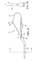
- a forward section of a catalyzer sensor connector is generally shown at 2, comprising a forward conical housing part 4, two half shells 6 and 8, a clamping ring 10, an outer shell 12, a cup spring 14, an outer casing 16 with a polarizing projection 17, and terminals 18.
- the forward connector part 2 is shown embedded in the metallic housing (only partially shown) of a catalyzer 1, the catalyzer 1 having a conical cavity 3 that mates with the outer conical surface 5 of the forward conical part 4, whereby the conical surfaces 5 and 3 serve not only to securely position the connector 2 with respect to the catalyzer 1, but also to seal off the hot exhaust gases from leaking to the exterior of the catalyzer 1.
- the spring 14 pushes against the two half shells 6 and 8 which correspondingly push onto the forward housing part 4.
- the opposing reactional force of the spring 14 is taken up by the casing 16, made of metal and laser welded on it's forward portion 15 to the catalyzer body 1.
- the casing 16 encompasses the two half shells 6, 8 and is polarized with respect thereto by engagement of the projection 17 in a corresponding longitudinal groove 19 on the half shell 6 outer periphery.
- the two half shells 6 and 8 and the forward conical part 4 not only need to be of dielectric material but must also withstand the high exhaust gas temperatures and are therefore made of ceramic material. Due to the difficulties of manufacturing and assembling the ceramic parts, the housing is separated into the forward conical part 4 and two halves 6 and 8, whereby a clamping ring 10 is provided to hold the two half shells 6 and 8 together.
- the connector 2 is shown having a slot 20 for reception of a ceramic printed circuit board 22 on which are deposited electrical circuit traces, electrical contact being made to the printed circuit board by terminals 18.
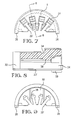
- the terminals 18 are retained within cavities 24 of the half shells 6 and 8 in a compact radial arrangement around the printed circuit board 22 as shown in Figure 2.
- projections 26 on the half shell 8 and corresponding cavities 28 on the half shell 6 that serve to correctly locate the half shell 8 to the half shell 6.
- the conical forward part 4 is shown in more detail with the printed circuit board receiving slot 20, the conical mounting surface 5 and at the rear end a projection 30 that engages with a recess 32 of the half shells 6 and 8, as shown in Figure 8, whereby this engagement positions and prevents rotation of the half shells 6, 8 with relation to the forward part 4.
- the projection 26 ( Figures 7, 8, 9) locates within a corresponding recess 28 on the half shell 6 for correct positioning of the shell 6 with respect to the shell 8, the shell halves being held together by the clamping ring 10 which is seated in an annular groove 34.
- Within the shell halves are cavities 24 disposed in a radial manner around the printed circuit board receiving slot 20, the cavity 24 having a shoulder 36 for the purpose of retaining the terminals 18 within the cavity 24.
- the sensor connector 2 should disturb as little as possible the structural integrity of the catalytic converter structure and also not cause any gas leakage, this essentially meaning that the connector 2 should be as small as possible, in particular the diameter of the conical opening 3.
- the width of the printed circuit board 22 must be correspondingly small. This however poses a problem of access to the circuit traces by the terminals 18 if they are to be aligned in a row. By disposing the terminals in a radial manner however, one can use the greater volume at the outer diameter of the connector but nevertheless making contact with the printed circuit board 22 by extending a contact arm 36.
- the contact arm 36 has a longitudinal arcuate contact projection 38 with a transverse arcuate contacting profile 40 that can maintain a tangential contact with the printed circuit board through different angles of the terminals 18 with respect thereto.
- the profile 40 is substantially circular.
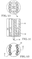
- the terminal 18 is shown in greater detail in Figures 10 and 11.
- the terminal 18 is stamped and formed from sheet metal and comprises the U-shaped resilient contact arm 36, a locking lance 41, a retaining projection 42 and a tab terminal section 44.
- the contacting surface 40 makes electrical contact with the printed circuit board 22 by being resiliently biased thereagainst.
- the longitudinal contact projection 38 with its longitudinal outwardly projecting arcuate profile, ensures that contact with the printed circuit board is always made thereagainst at a tangent to the profile 38 when manufacturing inaccuracies such as the printed circuit board thickness or position of the terminals 18 vary the position and angle of the contact arm 36, respectively contact projection 38.
- the contact arm 36 has a bent free end 37 that increases the resilient strength of the contact arm 36 during insertion of the printed circuit board into the slot 20, by pressing against the middle section 39 of the terminal 18.
- the resilient locking lance 41 is resiliently biased under the shoulder 36 during insertion of the terminal 18 into the cavity 24 and then springs open once past the shoulder to abut thereagainst preventing rearward extraction of the terminal, and a forward retaining projection 42 on the terminal abuts against the opposing side of the shoulder 36 to prevent forward movement of the terminal 18.
- a flat tab terminal 44 which is strengthened by folding the sheet metal into double thickness.
- the tab terminal 44 projects rearwards of the half shells 6 and 8 and serves to make electrical contact with receptacle terminals 51 assembled in a second housing 50, this housing also having a outer casing 52 that is attached to the casing 16 as shown in Figure 12.
- the second connector section 50 allows the first connector section 2 to be assembled separately to the catalytic converter 1 and in an ulterior step, connected to the second section 50 which makes electrical connection between the terminals 18 and electrical conducting wires 54. Because of the poor thermal conductivity of the ceramic material from which the forward conical part 4 and the shell halves 6 and 8 are formed, heat flow from the front to the rear of the first connector section 2 is very small and the second connector section 50 can therefore be maintained cool enough to allow use of a plastic housing 56; a one piece plastic injection molding which is far cheaper to manufacture than the ceramic parts 4, 6 and 8.
- the dielectric housing 56 has a locating pin 58 that fits into the recess 25 of the half shells, the pin 58 and corresponding recess 25 serving to correctly polarize the second connector section 50 with relation to the first connector section 2.
- terminal receiving cavities 62 are disposed in alignment with the terminals 18.
- the casing 52 during final assembly, is welded by laser at a overlapping position 64 to the casing 16 of the first section.
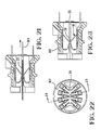
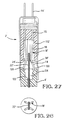
- FIG. 22 and 23 another embodiment of the invention is shown whereby the two half shells are replaced by a single ceramic part 102 within which the terminals 18 are locked in a similar manner to the embodiment of Figures 1 to 16. All other features of this embodiment are similar and denoted with the same numbering.
- the embodiment comprising the half shells 6 and 8, had the advantage of providing parts that can be manufactured easier than the single housing of the second embodiment 102, the half shells 6 and 8 also providing for assembly of the terminals directly onto the ceramic printed circuit board 20 without having to insert the board between the contacts 38 whereby the sharp broken edges of the ceramic could damage or remove the gold plating thereof.
- a special tool generally shown at 104 in Figures 24 and 25 comprises an inner plate member 106 of substantially the same thickness as the printed circuit board 20, and a pair of thin outer plate members 108 that could be made, for example, out of stainless steel.
- the inner plate member 106 has a tapered forward end 110.
- the outer plate members have smoothly rounded forward tips 112.
- the tool 104 is first inserted into the rear of the ceramic shell 102 in the slot 20 provided for the printed circuit board 22 until the front cantilevered portions 112 of the thin outer plates 108 abut the contact portions 38 of the terminals 18. Due to the smoothly rounded tips 112 of the external plate 108, on contact with the contact portions 38 the cantilevered front portions 112 are biased together and inserted between the contacts 38 as shown in Figure 18.
- the tool is then further inserted until the front end 112 projects past the front end of the ceramic body 102 for reception of the printed circuit board 22 whereby the forward cantilevered portion 114 of the external plates 108 are biased away from each other by magnetic means or elastic pre-stressing thereof, such that the printed circuit board can be inserted between the rounded tips 112 and urged towards the inner plate 106 until it abuts the forward portion 110.
- the printed circuit board 22 and the tool 104 can then be retracted through the body 102 until the printed circuit board is correctly positioned therein and the tool can be removed as shown in Figure 21. Due to the thin cantilevered plate portions 114 that overlap the front edge of the printed circuit board 22 during insertion thereof between the terminals 18, the gold plated contacts 38 are protected from damage therefrom.
- a catalytic converter sensor connector 2' for making electrical connection to a ceramic printed circuit board 22' comprises a forward part 4' mountable to a structure, and a terminal receiving housing 102' formed of a single ceramic body. Mounted within the housing 102', are terminals 18' produced from circular wire. Within the housing 102', is a cavity 24' through which the terminals 18' extend, the cavity 24' also for receiving the printed circuit board 22' therein.
- the terminals 18' are disposed in a radial manner about the printed circuit board 22' for the same reasons as described in the above embodiments.
- the terminal 18' comprises an outer pin terminal section 44' for electrically contacting a complementary conductor, a mid-section 115 set within cavities of the housing 102' such that the terminals 18' cannot rotate, extending therefrom a printed circuit board contact section 116 having contacts 38', and extending therefrom a contact actuation lever arm 118 having curved-in ends 120.
- the forward ceramic housing 4' to which the printed circuit board 22' is bonded 122 comprises a cavity 124 surrounding a certain length of the printed circuit board 22' and having a tapered lead-in camming portion 126 for engagement with the lever arms 118 of the terminals 18'.
Landscapes
- Coupling Device And Connection With Printed Circuit (AREA)
- Manufacturing Of Electrical Connectors (AREA)
Description
Claims (15)
- A circular sensor connector (2, 2', 50) comprising a plurality of longitudinally extending terminals (18, 18') for electrical connection to a longitudinally extending internal planar printed circuit board (22, 22'), characterized in that the terminals (18, 18') are disposed in a radial manner around the printed circuit board (22, 22') with respect to the longitudinal direction, for reducing the diameter of the connector.
- The connector of claim 1 characterized in that the terminals (18) have an arcuate contact profile (40), when viewing in the longitudinal direction, that tangentially contacts the printed circuit board (22).
- The connector of claim 2 characterized in that the arcuate contact (40) is substantially circular.
- The connector of claims 2 or 3 characterized in that the arcuate contact profile (40) is transverse to a longitudinal arcuate contact projection (38) that accommodates various inaccuracies in the position and angle of the projection (38) with respect to the printed circuit board.
- The connector of any of claims 1-4 characterized in that the terminals (18) are insertable into cavities (24) of a forward connector part (2) whereby tab sections (44) of the terminals (18) project rearwardly of the forward part (2) and are conductible with terminals (51) of a second connector section (50).
- The connector of any of claims 1-5 characterized in that the terminal (18) are stamped and formed from sheet metal and each terminal (18) comprises a resilient contacting arm having a contact projection (38), a middle section (39), retention means (41, 42) and a tab terminal section (44), whereby the contact arm (36) is forwardly bent in a U-shaped form from the top of the middle section (39) to a free end (37) that is cooperable with the middle section (39) to increase resilient strength of the contact arm (36), and the tab terminal section (44) projects from the bottom of the middle section (39), the tab terminal (44) folded into double thickness of the sheet metal.
- The connector of claim 1 characterized in that the plurality of terminals (18) are all identical.
- The connector of claim 1 characterized in that the connector (2, 50) has a forward connector part (2) comprising the plurality of terminals (18) electrically connectable to mating terminals (51) comprised in the second section (50), the terminals (51) disposed in a radial manner for alignment to the terminals (18).
- The connector of claim 1 characterized in that the terminals (18') are preformed such that contacts (38') thereof are spaced away from either side of the printed circuit board during initial insertion thereof therebetween, the terminals (18') comprising forward lever arm (118) and camming portions (120) engageable with tapered camming surfaces (126) on a forward connector part (4') during assembly of the connector (2') such that the terminal contacts (38') are biased into the contact with circuit traces on the printed circuit board (22').
- The connector of claim 9 characterized in that the connector (2') comprises a terminal receiving housing (102') to which the terminals (18') are mounted, and the forward part (4') to which the PCB (22') is securely fixed (122), the forward part (4') comprising a cavity (124) surrounding the PCB (22') and facing the terminal receiving housing (102'), the cavity (124) comprising the camming surface (126) proximate a terminal receiving end thereof, whereby the terminal camming portions are received within the cavity (124) once the connector (2') is assembled.
- The connector of any of claims 1 to 5 and 7 to 10, characterized in that the terminals (18') are made from cylindrical wire.
- A method of assembling an internal printed circuit board (22) to the circular sensor connector of any of claims 1 to 11, comprising the steps of:providing a connector body (102) comprising a slot (20) therein for receiving the printed circuit board (22) and said terminals (18) mounted therein and comprising contact portions (38) for making electrical contact to electrical traces on the printed circuit board (22);providing a board insertion tool (104); inserting the tool (104) from a rear end of the connector body (102) into the slot (20) until a front end (110) thereof projects past a front end of the slot (20); andurging the printed circuit board (22) against the tool front end (110) whilst inserting the printed circuit board (22) into the slot (20) and between the contact portions (38).
- The method of claim 12 characterized in that the tool (104) comprises an inner plate member (106) and external plate members (108) adjacent opposing sides thereof, the external plate members (108) comprising a front cantilevered portion (114) projecting past a forward end (110) of the inner plate (106).
- The method of claim 13 characterized in that the inner plate member (106) is of substantially the same thickness as the printed circuit board (22), and the external plate members (108) are thin and flexible.
- The method of claim 13 or 14 characterized in that prior to urging the printed circuit board (22) against the tool front end (110), biasing apart the front cantilevered portion (114) of the external plate members (108).
Applications Claiming Priority (6)
| Application Number | Priority Date | Filing Date | Title |
|---|---|---|---|
| GB9303501 | 1993-02-22 | ||
| GB939303501A GB9303501D0 (en) | 1993-02-22 | 1993-02-22 | Electrical connector for sensor |
| GB9313967 | 1993-07-06 | ||
| GB939313967A GB9313967D0 (en) | 1993-07-06 | 1993-07-06 | Catalytic converter sensor connector |
| GB939316495A GB9316495D0 (en) | 1993-08-09 | 1993-08-09 | Catalytic converter sensor connector |
| GB9316495 | 1993-08-09 |
Publications (2)
| Publication Number | Publication Date |
|---|---|
| EP0613216A1 EP0613216A1 (en) | 1994-08-31 |
| EP0613216B1 true EP0613216B1 (en) | 1998-04-22 |
Family
ID=27266591
Family Applications (1)
| Application Number | Title | Priority Date | Filing Date |
|---|---|---|---|
| EP94102596A Expired - Lifetime EP0613216B1 (en) | 1993-02-22 | 1994-02-21 | Catalytic converter sensor connector |
Country Status (4)
| Country | Link |
|---|---|
| US (1) | US5435735A (en) |
| EP (1) | EP0613216B1 (en) |
| JP (1) | JPH06251835A (en) |
| DE (1) | DE69409698T2 (en) |
Families Citing this family (9)
| Publication number | Priority date | Publication date | Assignee | Title |
|---|---|---|---|---|
| DE29703729U1 (en) * | 1996-09-11 | 1997-05-15 | Augat Components GmbH, 53840 Troisdorf | Construction of a lambda module with mating connector |
| DE19828314C1 (en) * | 1998-06-25 | 2000-02-24 | Bosch Gmbh Robert | Method and device for connecting a probe to a printed circuit board with a connector consisting of two half-shells |
| US20060091006A1 (en) * | 1999-11-04 | 2006-05-04 | Yi Wang | Analyte sensor with insertion monitor, and methods |
| US6616819B1 (en) * | 1999-11-04 | 2003-09-09 | Therasense, Inc. | Small volume in vitro analyte sensor and methods |
| DE20020379U1 (en) * | 2000-12-01 | 2002-05-16 | Robert Bosch Gmbh, 70469 Stuttgart | Small coupling connector, especially for a planar broadband lambda probe |
| DE20020373U1 (en) * | 2000-12-01 | 2002-04-04 | Robert Bosch Gmbh, 70469 Stuttgart | Harness connector, especially as a planar two-cell limit current probe with molded cover element |
| DE10253517B3 (en) * | 2002-11-16 | 2004-05-13 | Phoenix Contact Gmbh & Co. Kg | Spring clamp used as electrical component plug has operating element acted on by external tool for opening clamp windows for insertion or removal of component current leads |
| JP6981948B2 (en) * | 2018-09-25 | 2021-12-17 | 日本特殊陶業株式会社 | Gas sensor |
| CN112086779B (en) * | 2020-07-29 | 2021-11-05 | 深圳市粤电新能源技术有限公司 | PCB (printed circuit board) end connecting wire structure of charging gun |
Citations (1)
| Publication number | Priority date | Publication date | Assignee | Title |
|---|---|---|---|---|
| EP0493801A2 (en) * | 1991-01-03 | 1992-07-08 | Burndy Corporation | Bi-level card edge connector with selectively movable contacts for use with different types of cards |
Family Cites Families (12)
| Publication number | Priority date | Publication date | Assignee | Title |
|---|---|---|---|---|
| US3425021A (en) * | 1966-07-28 | 1969-01-28 | Rca Corp | Method and apparatus for connecting leads to a printed circuit board |
| IT975428B (en) * | 1972-10-31 | 1974-07-20 | Fiat Spa | WATERPROOF CONNECTOR BETWEEN CABLES AND MOLDED CIR CUITS |
| FR2261680A1 (en) * | 1974-02-14 | 1975-09-12 | Tech Europ Commutati | Printed circuit card connector strip - provides symmetrical contact pressure from a single piece socket |
| DE2805598A1 (en) * | 1978-02-10 | 1979-08-16 | Bbc Brown Boveri & Cie | Electrochemical oxygen sensor for IC engine exhaust gases - has air inlet for protection of solid electrolyte tube |
| EP0036933A3 (en) * | 1980-03-28 | 1981-12-02 | Bohdan Ulrich | Pluggable connector and its use in making a disconnectible electrical connection |
| DE3210804A1 (en) * | 1982-03-24 | 1983-10-06 | Blaupunkt Werke Gmbh | Connection holder with spark gaps for a cathode ray tube, particularly a picture tube |
| US4621882A (en) * | 1984-05-14 | 1986-11-11 | Beta Phase, Inc. | Thermally responsive electrical connector |
| GB8725475D0 (en) * | 1987-10-30 | 1987-12-02 | Amp Holland | Modular jack |
| US4850882A (en) * | 1987-12-28 | 1989-07-25 | Wenli Yu | Rotatably mounted printed circuit board test support and connector |
| JPH01187444A (en) * | 1988-01-21 | 1989-07-26 | Shimadzu Corp | Card type ammonia sensor and its measuring device |
| US4941830A (en) * | 1988-08-01 | 1990-07-17 | International Business Machines Corp. | Edge design for printed circuit board connector |
| US5108315A (en) * | 1991-04-22 | 1992-04-28 | International Teleservice Corporation | Pay telephone station repair technician's adapter |
-
1994
- 1994-02-10 US US08/194,597 patent/US5435735A/en not_active Expired - Fee Related
- 1994-02-21 EP EP94102596A patent/EP0613216B1/en not_active Expired - Lifetime
- 1994-02-21 DE DE69409698T patent/DE69409698T2/en not_active Expired - Fee Related
- 1994-02-22 JP JP6047848A patent/JPH06251835A/en active Pending
Patent Citations (1)
| Publication number | Priority date | Publication date | Assignee | Title |
|---|---|---|---|---|
| EP0493801A2 (en) * | 1991-01-03 | 1992-07-08 | Burndy Corporation | Bi-level card edge connector with selectively movable contacts for use with different types of cards |
Also Published As
| Publication number | Publication date |
|---|---|
| EP0613216A1 (en) | 1994-08-31 |
| DE69409698T2 (en) | 1998-09-17 |
| US5435735A (en) | 1995-07-25 |
| JPH06251835A (en) | 1994-09-09 |
| DE69409698D1 (en) | 1998-05-28 |
Similar Documents
| Publication | Publication Date | Title |
|---|---|---|
| KR0128487B1 (en) | Electrical connector system | |
| US7033216B2 (en) | Watertight connector | |
| US3497866A (en) | Electrical connector | |
| CN100461533C (en) | electrical connector | |
| US5482474A (en) | Edge-mountable circuit board connector | |
| US7367811B2 (en) | Coaxial cable connector | |
| JP2935493B2 (en) | General purpose connector for thermocouple | |
| US5435735A (en) | Catalytic converter sensor connector | |
| CA1197909A (en) | Connector assembly | |
| US4664467A (en) | Coaxial cable terminator | |
| US20040110425A1 (en) | Electrical connector capable of preventing plugging error | |
| JPH05283131A (en) | Surface mount type connector | |
| EP0592519A1 (en) | Dual usage electrical/electronic pin terminal system | |
| US20050026474A1 (en) | Electrical connector having improved terminals | |
| JPS61296671A (en) | Connector and socket module | |
| US20010044236A1 (en) | Electrical connector with female contact element | |
| EP0345788B1 (en) | Detachable probe-type electronic clinical thermometer | |
| CA1101953A (en) | Interconnection between printed circuit board panels and external components | |
| US6056599A (en) | Electrical connector with matable contact assembly | |
| JPH08148205A (en) | Printed board terminal | |
| US6254402B1 (en) | Push pin ground | |
| US20040266229A1 (en) | Electrical connector having a spacer | |
| JPH11111414A (en) | Valve socket and method of manufacturing the same | |
| JP3929948B2 (en) | connector | |
| JP2654498B2 (en) | Electrical connector assembly and electrical terminal |
Legal Events
| Date | Code | Title | Description |
|---|---|---|---|
| PUAI | Public reference made under article 153(3) epc to a published international application that has entered the european phase |
Free format text: ORIGINAL CODE: 0009012 |
|
| AK | Designated contracting states |
Kind code of ref document: A1 Designated state(s): DE FR GB IT SE |
|
| 17P | Request for examination filed |
Effective date: 19950215 |
|
| 17Q | First examination report despatched |
Effective date: 19960702 |
|
| GRAG | Despatch of communication of intention to grant |
Free format text: ORIGINAL CODE: EPIDOS AGRA |
|
| GRAG | Despatch of communication of intention to grant |
Free format text: ORIGINAL CODE: EPIDOS AGRA |
|
| GRAH | Despatch of communication of intention to grant a patent |
Free format text: ORIGINAL CODE: EPIDOS IGRA |
|
| GRAH | Despatch of communication of intention to grant a patent |
Free format text: ORIGINAL CODE: EPIDOS IGRA |
|
| GRAA | (expected) grant |
Free format text: ORIGINAL CODE: 0009210 |
|
| AK | Designated contracting states |
Kind code of ref document: B1 Designated state(s): DE FR GB IT SE |
|
| PG25 | Lapsed in a contracting state [announced via postgrant information from national office to epo] |
Ref country code: IT Free format text: LAPSE BECAUSE OF FAILURE TO SUBMIT A TRANSLATION OF THE DESCRIPTION OR TO PAY THE FEE WITHIN THE PRE;WARNING: LAPSES OF ITALIAN PATENTS WITH EFFECTIVE DATE BEFORE 2007 MAY HAVE OCCURRED AT ANY TIME BEFORE 2007. THE CORRECT EFFECTIVE DATE MAY BE DIFFERENT FROM THE ONE RECORDED.SCRIBED TIME-LIMIT Effective date: 19980422 |
|
| REF | Corresponds to: |
Ref document number: 69409698 Country of ref document: DE Date of ref document: 19980528 |
|
| ET | Fr: translation filed | ||
| PG25 | Lapsed in a contracting state [announced via postgrant information from national office to epo] |
Ref country code: SE Free format text: LAPSE BECAUSE OF FAILURE TO SUBMIT A TRANSLATION OF THE DESCRIPTION OR TO PAY THE FEE WITHIN THE PRESCRIBED TIME-LIMIT Effective date: 19980722 |
|
| PLBE | No opposition filed within time limit |
Free format text: ORIGINAL CODE: 0009261 |
|
| STAA | Information on the status of an ep patent application or granted ep patent |
Free format text: STATUS: NO OPPOSITION FILED WITHIN TIME LIMIT |
|
| 26N | No opposition filed | ||
| PGFP | Annual fee paid to national office [announced via postgrant information from national office to epo] |
Ref country code: GB Payment date: 19991224 Year of fee payment: 7 |
|
| PGFP | Annual fee paid to national office [announced via postgrant information from national office to epo] |
Ref country code: DE Payment date: 19991229 Year of fee payment: 7 |
|
| PGFP | Annual fee paid to national office [announced via postgrant information from national office to epo] |
Ref country code: FR Payment date: 20000207 Year of fee payment: 7 |
|
| PG25 | Lapsed in a contracting state [announced via postgrant information from national office to epo] |
Ref country code: GB Free format text: LAPSE BECAUSE OF NON-PAYMENT OF DUE FEES Effective date: 20010221 |
|
| GBPC | Gb: european patent ceased through non-payment of renewal fee |
Effective date: 20010221 |
|
| PG25 | Lapsed in a contracting state [announced via postgrant information from national office to epo] |
Ref country code: FR Free format text: LAPSE BECAUSE OF NON-PAYMENT OF DUE FEES Effective date: 20011031 |
|
| REG | Reference to a national code |
Ref country code: FR Ref legal event code: ST |
|
| PG25 | Lapsed in a contracting state [announced via postgrant information from national office to epo] |
Ref country code: DE Free format text: LAPSE BECAUSE OF NON-PAYMENT OF DUE FEES Effective date: 20011201 |