EP0610779B1 - Anordnung und Verfahren zur Erzeugung des "sticky bits" in Gleitkommaoperation durch Zweirichtungsausbreitung der Gruppenfreigaben - Google Patents
Anordnung und Verfahren zur Erzeugung des "sticky bits" in Gleitkommaoperation durch Zweirichtungsausbreitung der Gruppenfreigaben Download PDFInfo
- Publication number
- EP0610779B1 EP0610779B1 EP19940101470 EP94101470A EP0610779B1 EP 0610779 B1 EP0610779 B1 EP 0610779B1 EP 19940101470 EP19940101470 EP 19940101470 EP 94101470 A EP94101470 A EP 94101470A EP 0610779 B1 EP0610779 B1 EP 0610779B1
- Authority
- EP
- European Patent Office
- Prior art keywords
- group
- bits
- groups
- bit
- sticky bit
- Prior art date
- Legal status (The legal status is an assumption and is not a legal conclusion. Google has not performed a legal analysis and makes no representation as to the accuracy of the status listed.)
- Expired - Lifetime
Links
Images


Classifications
-
- G—PHYSICS
- G06—COMPUTING OR CALCULATING; COUNTING
- G06F—ELECTRIC DIGITAL DATA PROCESSING
- G06F7/00—Methods or arrangements for processing data by operating upon the order or content of the data handled
- G06F7/38—Methods or arrangements for performing computations using exclusively denominational number representation, e.g. using binary, ternary, decimal representation
- G06F7/48—Methods or arrangements for performing computations using exclusively denominational number representation, e.g. using binary, ternary, decimal representation using non-contact-making devices, e.g. tube, solid state device; using unspecified devices
- G06F7/483—Computations with numbers represented by a non-linear combination of denominational numbers, e.g. rational numbers, logarithmic number system or floating-point numbers
-
- G—PHYSICS
- G06—COMPUTING OR CALCULATING; COUNTING
- G06F—ELECTRIC DIGITAL DATA PROCESSING
- G06F7/00—Methods or arrangements for processing data by operating upon the order or content of the data handled
- G06F7/38—Methods or arrangements for performing computations using exclusively denominational number representation, e.g. using binary, ternary, decimal representation
- G06F7/48—Methods or arrangements for performing computations using exclusively denominational number representation, e.g. using binary, ternary, decimal representation using non-contact-making devices, e.g. tube, solid state device; using unspecified devices
- G06F7/499—Denomination or exception handling, e.g. rounding or overflow
- G06F7/49942—Significance control
- G06F7/49947—Rounding
- G06F7/49952—Sticky bit
Definitions
- This invention relates to floating point processing in computers, and more particularly to a method and apparatus for calculating the "sticky bit" in floating point operations.
- the final result of a floating point operation is a rounded quantity which is generated by the application of a rounding algorithm to an intermediate result.
- the task of the rounding algorithm is to convert an intermediate result whose width is possibly greater than n, to a representative quantity of width at most n.
- the values of the round((n+1)th bit), guard(n+2)th bit), and sticky bits must be known.
- the sticky bit is defined as the logical OR of all bits beyond the guard bit position.
- Non-zero bits beyond the guard bit position could be generated as a result of alignment shifts as in the case of add/subtract/convert operations, or by multiply/divide operations.
- the generation of the sticky bit for multiply operations can be mapped to an alignment shift case.
- This invention describes a technique to detect the sticky bit when generated as a result of alignment.
- the invention in its broad form includes a method of calculating a sticky bit in a floating point processor, generally as recited in claim 1.
- the invention also includes a circuit for calculating a sticky bit in a floating point processor as recited in claim 5.
- a floating point processor must recognize the fact that floating point units cannot always generate infinitely precise results, as they are constrained by implementation size to a certain degree of precision. Any result whose width is greater than the maximum allowable width for the given destination datatype format must be rounded and reported.
- the rounding algorithm needs to know the value of the (n+1)th and (n+2)th bits known as the round and guard bits respectively and in certain rounding schemes such as the IEEE round-to nearest/even (required by IEEE standard 754-1985). It needs information about the existence of any ones in the result beyond the (n+2)th position. The presence of "1's" beyond the (n+2)th position sets the "sticky bit.” Sticky bit detection is also required in order to correctly generate results in the case of subtract operations.
- a method is provided to detect the "sticky bit" when generated as a result of an alignment operation.
- the detection of the sticky bit is done in parallel with the alignment operation and uses parallel two way propagation of group enables. This scheme is significantly faster than conventional schemes that use serial one-way propagation of group enables.
- a floating point operation such as addition/subtraction in a block 10 accepts two n-bit inputs A and B, and produces an output C of width M, where M could be greater than n.
- M could be greater than n.
- the floating point representation of a number comprises a fraction "F" of some width "n” and an exponent "E” of some other width "r”.
- the fraction of the smaller of the two numbers must be aligned with the fraction associated with the larger number. This is achieved by right shifting the fraction associated with the smaller number by an amount determined by the exponent difference of the two numbers.
- Addition/subtraction of the shifted fraction F A and the unshifted fraction F B therefore can produce a fraction F (at output C) whose width can be greater than that of F A or F B .
- the datapaths and registers in the floating point processor are of some nominal width, such as 64-bits, so the output C (greater than 64-bit) must be rounded, producing 64-bit result.
- the rounding algorithm needs to know the value of the (n+1)th and (n+2)th bits, known as the round and guard bits respectively; in certain rounding schemes such as the IEEE round-to nearest/even (required by IEEE standard 754-1985), it needs information about the existence of any ones in the result beyond the (n+2)th position.
- the 16-bit output C contains a round-bit at bit-9, a guard-bit at bit-10, and bits 11-16 are examined to see if any "1's" are present.
- sticky bit detection is typically performed on the inputs.
- sticky bit detection on the output "C” would require a 16-bit datapath, whereas the datapath width need only be 10-bits, in order to generate appropriately rounded results.
- a scheme for sticky bit detection is to provide the two N bit vectors "F" and "S" as inputs 12 and 13 to the sticky bit logic 14.
- the sticky bit is computed as the OR of all bits in F register 15 to the right of the "1" in S register 16, using OR gate 17 to produce sticky bit output 18. Note that this is not actually implemented as a simple OR gate, as the position of the "1" in the S vector may vary and therefore, depending upon the position, the number of inputs to the OR gate 17 will vary.
- this OR-like structure is referred to as a VOR (variable OR gate) and use the symbol of an OR gate to represent it.
- the operation on the N-bit operand F is subdivided into p groups, each of which evaluate in parallel.
- p groups each of which evaluate in parallel.
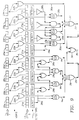
- the F input 12 is applied to three 4-bit registers 20a, 20b and 20c, and the S input is likewise split into three entities 21a, 21b and 21c.
- a VOR gate 22a, 22b and 22c makes an separate evaluation of each group, based on the S for that group, producing three sticky bit outputs 23a, 23b and 23c. These three bits are combined in a combine circuit described below, producing a single sticky bit output 25.
- a raw sticky bit STKY[i] is computed at outputs 23a, etc., for each group i, based on the earlier definition for the sticky bit, with one exception.
- groups with all zero "S" vectors 21a, 21b, or 21c Such groups may or may not contribute to the final sticky bit depending on the position of the "1" in the complete S vector. We initially assume that all such groups contribute to the sticky bit.
- a corrected sticky bit is then evaluated for each group which factors in the actual position of the "1" in the complete S vector.
- Group i is enabled (i.e., contributes to the final sticky bit) if the "1" in the S vector is in group i or in a group to the left.
- Group i is disabled if the 1 in the S vector is in a group to the right.
- an enable is generated on line 26a if there is a 1 in the corresponding vector 21a
- an enable is generated on line 26b if there is a 1 in the corresponding vector 21b, and so on.
- the corrected sticky bit for each group is then computed as the logical AND of the raw sticky bit STKY[i] and the enable E[i] for that group.
- the output 26c is applied to an AND gate 27c, with the raw sticky bit 23c as the other input, producing a corrected sticky bit on line 28c.
- the invention is thus a new scheme for the generation of group enable signals.
- the S vector is a decoded quantity and contains only a single "1.” If there is a "1" in the S vector to the left of bit position k, then all bits k through O in S must be zero.
- Group i is enabled if the "1" in the S vector is in group i OR in a group to the left" as used above is the statement "Group i is enabled if the S vectors of ALL groups to the right of group i are zero.”
- SZ[i] 0 if the S vector for that group is nonzero.
- SZ[i] NOT (SNZ[i]).
- the corrected sticky bits 30a, 30b, 30c and 30d are the logical AND provided by gates 31a, 31b, and 31c plus the value 26h, derived as explained above from the indications of whether the values 21e-21h contain a "1."
- An OR gate 32 produces a sticky bit output 33, which is ORed with the output of gate 29 to produce an overall sticky-bit output 35.
- this method of this invention can evaluate the group enables twice as fast. As the speed of the sticky bit calculation is determined partly by the group enables, this results in a significant performance gain in the overall sticky bit calculation.
- the parallel two-way propagation scheme helps speed up the computation of the group enables by a factor of two, i.e., 100%. Under the traditional scheme for the generation of group enables, any speedup could be attained only at the cost of additional chip area.
- the new scheme provides a fast and area-wise efficient scheme for the generation of the sticky bit.
Landscapes
- Engineering & Computer Science (AREA)
- General Physics & Mathematics (AREA)
- Physics & Mathematics (AREA)
- Mathematical Optimization (AREA)
- Computing Systems (AREA)
- Mathematical Analysis (AREA)
- Computational Mathematics (AREA)
- Pure & Applied Mathematics (AREA)
- Theoretical Computer Science (AREA)
- Nonlinear Science (AREA)
- General Engineering & Computer Science (AREA)
- Executing Machine-Instructions (AREA)
- Complex Calculations (AREA)
Claims (8)
- Verfahren zum Berechnen eines Sticky-Bits in einem Gleitkommaprozessor, mit den folgenden Schritten:gekennzeichnet durchUnterteilen eines Eingangswertes (F) in M Bitgruppen;Ausführen einer Verschiebung um einen Betrag von S Bits, wobei alle S Bits mit Ausnahme eines einzigen für die Position, die die Anzahl von Bits repräsentiert, deren Eingangswert verschoben werden soll, null sind;Unterteilen (21a-21h) des Betrages S in M Gruppen, wovon jede ein S-Vektor genannt wird, die den M Bitgruppen des unterteilten Eingangswertes entsprechen;Ausführen einer ersten Feststellung (1-DETECTORS) für jeden der S-Vektoren, ob darin eine "1" auftritt, um ein Gruppe-eins-Erfassungssignal zu erzeugen, das einer entsprechenden der M Bitgruppen zugeordnet ist;Ausführen einer zweiten Feststellung (22a-22h) für jede der M Bitgruppen, ob in der Bitgruppe rechts von einem Bit, das der Bitposition entspricht, die in dem dieser Gruppe zugeordneten S-Vektor eine "1" enthält, eine "1" vorhanden ist;für jede der M-x Bitgruppen hoher Ordnung der M Bitgruppen Erzeugen (26a-26d) eines Gruppenfreigabesignals (26a-26d), das dadurch bestimmt ist, ob das Gruppe-eins-Erfassungssignal in dem dieser Gruppe zugeordneten S-Vektor oder in irgendeinem S-Vektor, der einer Gruppe der M - x Bitgruppen hoher Ordnung oberhalb dieser Gruppe zugeordnet ist, auftritt;für jede der x Gruppen niedriger Ordnung der M Bitgruppen (20e-20h) Erzeugen eines Gruppenfreigabesignals (26e-26h), das dadurch bestimmt ist, ob das Gruppe-eins-Erfassungssignal in keiner Bitgruppe niedriger Ordnung rechts von dieser Gruppe vorhanden ist;für jede der M Bitgruppen Erzeugen (27, 31) eines jeweiligen Gruppen-Sticky-Bit-Signals anhand der Ergebnisse der zweiten Feststellung (23) für diese Bitgruppe in Verbindung mit dem Vorhandensein eines Gruppenfreigabesignals (26) für diese Bitgruppe; undErzeugen (29, 32, 34) einer Gesamt-Sticky-Bit-Angabe (35) aus sämtlichen Gruppen-Sticky-Bit-Signalen.
- Verfahren nach Anspruch 1, bei dem der Eingangswert durch zwei teilbar ist.
- Verfahren nach Anspruch 2, bei dem die Anzahl der Gruppen hoher Ordnung der M Bitgruppen (20a-20d) und die Anzahl der Gruppen niedriger Ordnung der M Bitgruppen (20e-20h) gleich sind.
- Verfahren nach Anspruch 1, bei dem die Erzeugungsschritte gleichzeitig ausgeführt werden.
- Schaltung zum Berechnen eines Sticky-Bits in einem Gleitkommaprozessor, mit:einer Einrichtung (20a-20h) zum Unterteilen eines Eingangswertes in M Bitgruppen;einer Einrichtung zum Schaffen eines Verschiebungsbetrages von S Bits, wobei sämtliche S Bits mit Ausnahme einer "1" an der Position, die eine Anzahl von Bits repräsentiert, um die der Eingangswert verschoben worden ist, null sind;einer Einrichtung zum Unterteilen (21a-21h) des Betrages S in M Gruppen, wovon jede ein S-Vektor genannt wird, die den M Bitgruppen des unterteilten Eingangswertes entsprechen;einer Detektoreinrichtung (1-DETECTORS) zum Ausführen einer ersten Feststellung für jeden der S-Vektoren, ob darin eine "1" auftritt, um ein Gruppe-eins-Erfassungssignal für die M Bitgruppen, das diesem S-Vektor zugeordnet ist, zu erzeugen;einer Vergleichseinrichtung (14) zum Ausführen einer zweiten Feststellung (22a-22h) für jede Gruppe der M Bitgruppen, ob in der Bitgruppe rechts von einem Bit, das der Bitposition entspricht, die in dem dieser Gruppe zugeordneten S-Vektor eine "1" enthält, eine "1" vorhanden ist; gekennzeichnet durcheine erste Einrichtung, die von der Detektoreinrichtung (1-DETECTORS) Eingangssignale empfängt, um für jede der M - x Gruppen höherer Ordnung der M Bitgruppen ein Gruppenfreigabesignal (26a-26d) zu erzeugen, das dadurch bestimmt ist, ob das Gruppe-eins-Erfassungssignal in dem dieser Gruppe zugeordneten S-Vektor oder in irgendeinem S-Vektor, der einer Gruppe der M - x Bitgruppen hoher Ordnung oberhalb dieser Gruppe zugeordnet ist, auftritt;eine zweite Einrichtung, die Eingangssignale von der Detektoreinrichtung (1-DETECTORS) empfängt, um für jede der x Bitgruppen niedriger Ordnung der M Bitgruppen (20e-20h) ein Gruppenfreigabesignal (26e-26h) zu erzeugen, das dadurch bestimmt ist, ob das Gruppe-eins-Erfassungssignal in keiner Bitgruppe niedriger Ordnung rechts von dieser Gruppe vorhanden ist;eine Logikschaltungsanordnung (27, 31) für jede der M Bitgruppen, die so angeschlossen ist, daß sie von der ersten Einrichtung, von der zweiten Einrichtung und von der Vergleichseinrichtung (14) Eingangssignale empfängt, um ein entsprechendes korrigiertes Sticky-BitSignal (28a-28d; 30a-30b) für jede der M Bitgruppen zu erzeugen; undeine Ausgangslogikschaltungsanordnung (29, 32, 34) zum Erzeugen einer Gesamt-Sticky-Bit-Angabe (35) aus sämtlichen korrigierten Sticky-Bit-Signalen.
- Schaltung nach Anspruch 5, bei der der Eingangswert durch zwei teilbar ist.
- Schaltung nach Anspruch 6, bei der die Bitgruppen hoher Ordnung der M - x Bitgruppen und die Bitgruppen niedriger Ordnung der x Bitgruppen der Anzahl nach gleich sind.
- Schaltung nach Anspruch 5, bei der die erste und die zweite Einrichtung so betreibbar sind, daß sie die Gruppenfreigabesignale gleichzeitig erzeugen.
Applications Claiming Priority (2)
| Application Number | Priority Date | Filing Date | Title |
|---|---|---|---|
| US1605793A | 1993-02-10 | 1993-02-10 | |
| US16057 | 1993-02-10 |
Publications (2)
| Publication Number | Publication Date |
|---|---|
| EP0610779A1 EP0610779A1 (de) | 1994-08-17 |
| EP0610779B1 true EP0610779B1 (de) | 1999-12-22 |
Family
ID=21775145
Family Applications (1)
| Application Number | Title | Priority Date | Filing Date |
|---|---|---|---|
| EP19940101470 Expired - Lifetime EP0610779B1 (de) | 1993-02-10 | 1994-02-01 | Anordnung und Verfahren zur Erzeugung des "sticky bits" in Gleitkommaoperation durch Zweirichtungsausbreitung der Gruppenfreigaben |
Country Status (2)
| Country | Link |
|---|---|
| EP (1) | EP0610779B1 (de) |
| DE (1) | DE69422206T2 (de) |
Families Citing this family (1)
| Publication number | Priority date | Publication date | Assignee | Title |
|---|---|---|---|---|
| CN100336014C (zh) * | 2004-05-12 | 2007-09-05 | 中国人民解放军国防科学技术大学 | 并行粘接位计算部件设计方法 |
-
1994
- 1994-02-01 EP EP19940101470 patent/EP0610779B1/de not_active Expired - Lifetime
- 1994-02-01 DE DE1994622206 patent/DE69422206T2/de not_active Expired - Fee Related
Also Published As
| Publication number | Publication date |
|---|---|
| EP0610779A1 (de) | 1994-08-17 |
| DE69422206T2 (de) | 2000-08-03 |
| DE69422206D1 (de) | 2000-01-27 |
Similar Documents
| Publication | Publication Date | Title |
|---|---|---|
| US5027308A (en) | Circuit for adding/subtracting two floating point operands | |
| US6529928B1 (en) | Floating-point adder performing floating-point and integer operations | |
| US5241490A (en) | Fully decoded multistage leading zero detector and normalization apparatus | |
| US5010508A (en) | Prenormalization for a floating-point adder | |
| AU628969B2 (en) | Pipelined floating point adder for digital computer | |
| WO2001046795A2 (en) | Method and apparatus for performing single-cycle addition or subtraction and comparison in redundant form arithmetic | |
| US4928259A (en) | Sticky bit predictor for floating-point multiplication | |
| US5341319A (en) | Method and apparatus for controlling a rounding operation in a floating point multiplier circuit | |
| US6205462B1 (en) | Digital multiply-accumulate circuit that can operate on both integer and floating point numbers simultaneously | |
| US4941119A (en) | Method and apparatus for predicting an overflow in an integer multiply | |
| US4639887A (en) | Bifurcated method and apparatus for floating point addition with decreased latency time | |
| JPH05224883A (ja) | 浮動小数点n−ビット符号付大きさの2進数を固定小数点m−ビット2の補数表示の2進数に変換するためのシステム | |
| US7290023B2 (en) | High performance implementation of exponent adjustment in a floating point design | |
| EP0610779B1 (de) | Anordnung und Verfahren zur Erzeugung des "sticky bits" in Gleitkommaoperation durch Zweirichtungsausbreitung der Gruppenfreigaben | |
| JPH02294731A (ja) | 浮動小数点数演算処理装置及び除数倍数生成装置 | |
| US20070050434A1 (en) | Data processing apparatus and method for normalizing a data value | |
| US5920493A (en) | Apparatus and method to determine a most significant bit | |
| US5432727A (en) | Apparatus for computing a sticky bit for a floating point arithmetic unit | |
| KR101922462B1 (ko) | 데이터 처리장치 및 이진수에 대해 시프트 기능을 수행하는 방법 | |
| US7016928B2 (en) | Floating point status information testing circuit | |
| US7003540B2 (en) | Floating point multiplier for delimited operands | |
| US5408427A (en) | Detection of exponent underflow and overflow in a floating point adder | |
| JP3257278B2 (ja) | 冗長なシフト数予測とシフト誤り補正を用いた正規化装置 | |
| US7599974B2 (en) | Data processing apparatus and method for comparing floating point operands | |
| US6044391A (en) | Method of generating the sticky-bit from the input operands |
Legal Events
| Date | Code | Title | Description |
|---|---|---|---|
| PUAI | Public reference made under article 153(3) epc to a published international application that has entered the european phase |
Free format text: ORIGINAL CODE: 0009012 |
|
| AK | Designated contracting states |
Kind code of ref document: A1 Designated state(s): DE FR GB IT |
|
| 17P | Request for examination filed |
Effective date: 19941207 |
|
| 17Q | First examination report despatched |
Effective date: 19980617 |
|
| GRAG | Despatch of communication of intention to grant |
Free format text: ORIGINAL CODE: EPIDOS AGRA |
|
| GRAG | Despatch of communication of intention to grant |
Free format text: ORIGINAL CODE: EPIDOS AGRA |
|
| GRAG | Despatch of communication of intention to grant |
Free format text: ORIGINAL CODE: EPIDOS AGRA |
|
| GRAH | Despatch of communication of intention to grant a patent |
Free format text: ORIGINAL CODE: EPIDOS IGRA |
|
| GRAH | Despatch of communication of intention to grant a patent |
Free format text: ORIGINAL CODE: EPIDOS IGRA |
|
| GRAA | (expected) grant |
Free format text: ORIGINAL CODE: 0009210 |
|
| AK | Designated contracting states |
Kind code of ref document: B1 Designated state(s): DE FR GB IT |
|
| PG25 | Lapsed in a contracting state [announced via postgrant information from national office to epo] |
Ref country code: IT Free format text: LAPSE BECAUSE OF FAILURE TO SUBMIT A TRANSLATION OF THE DESCRIPTION OR TO PAY THE FEE WITHIN THE PRE;WARNING: LAPSES OF ITALIAN PATENTS WITH EFFECTIVE DATE BEFORE 2007 MAY HAVE OCCURRED AT ANY TIME BEFORE 2007. THE CORRECT EFFECTIVE DATE MAY BE DIFFERENT FROM THE ONE RECORDED.SCRIBED TIME-LIMIT Effective date: 19991222 |
|
| REF | Corresponds to: |
Ref document number: 69422206 Country of ref document: DE Date of ref document: 20000127 |
|
| PGFP | Annual fee paid to national office [announced via postgrant information from national office to epo] |
Ref country code: DE Payment date: 20000131 Year of fee payment: 7 |
|
| PGFP | Annual fee paid to national office [announced via postgrant information from national office to epo] |
Ref country code: FR Payment date: 20000210 Year of fee payment: 7 |
|
| ET | Fr: translation filed | ||
| REG | Reference to a national code |
Ref country code: GB Ref legal event code: 732E |
|
| PLBE | No opposition filed within time limit |
Free format text: ORIGINAL CODE: 0009261 |
|
| STAA | Information on the status of an ep patent application or granted ep patent |
Free format text: STATUS: NO OPPOSITION FILED WITHIN TIME LIMIT |
|
| 26N | No opposition filed | ||
| PG25 | Lapsed in a contracting state [announced via postgrant information from national office to epo] |
Ref country code: FR Free format text: LAPSE BECAUSE OF NON-PAYMENT OF DUE FEES Effective date: 20011031 |
|
| REG | Reference to a national code |
Ref country code: FR Ref legal event code: ST |
|
| PG25 | Lapsed in a contracting state [announced via postgrant information from national office to epo] |
Ref country code: DE Free format text: LAPSE BECAUSE OF NON-PAYMENT OF DUE FEES Effective date: 20011201 |
|
| REG | Reference to a national code |
Ref country code: GB Ref legal event code: IF02 |
|
| PGFP | Annual fee paid to national office [announced via postgrant information from national office to epo] |
Ref country code: GB Payment date: 20070223 Year of fee payment: 14 |
|
| GBPC | Gb: european patent ceased through non-payment of renewal fee |
Effective date: 20080201 |
|
| PG25 | Lapsed in a contracting state [announced via postgrant information from national office to epo] |
Ref country code: GB Free format text: LAPSE BECAUSE OF NON-PAYMENT OF DUE FEES Effective date: 20080201 |