EP0609921A2 - Oxide superconductor and method of manufacturing the same - Google Patents
Oxide superconductor and method of manufacturing the same Download PDFInfo
- Publication number
- EP0609921A2 EP0609921A2 EP19940107698 EP94107698A EP0609921A2 EP 0609921 A2 EP0609921 A2 EP 0609921A2 EP 19940107698 EP19940107698 EP 19940107698 EP 94107698 A EP94107698 A EP 94107698A EP 0609921 A2 EP0609921 A2 EP 0609921A2
- Authority
- EP
- European Patent Office
- Prior art keywords
- oxide superconductor
- superconductor
- oxide
- metal
- layer
- Prior art date
- Legal status (The legal status is an assumption and is not a legal conclusion. Google has not performed a legal analysis and makes no representation as to the accuracy of the status listed.)
- Granted
Links
Images


Classifications
-
- H—ELECTRICITY
- H10—SEMICONDUCTOR DEVICES; ELECTRIC SOLID-STATE DEVICES NOT OTHERWISE PROVIDED FOR
- H10N—ELECTRIC SOLID-STATE DEVICES NOT OTHERWISE PROVIDED FOR
- H10N60/00—Superconducting devices
- H10N60/01—Manufacture or treatment
- H10N60/0268—Manufacture or treatment of devices comprising copper oxide
- H10N60/0801—Processes peculiar to the manufacture or treatment of filaments or composite wires
-
- H—ELECTRICITY
- H10—SEMICONDUCTOR DEVICES; ELECTRIC SOLID-STATE DEVICES NOT OTHERWISE PROVIDED FOR
- H10N—ELECTRIC SOLID-STATE DEVICES NOT OTHERWISE PROVIDED FOR
- H10N60/00—Superconducting devices
- H10N60/20—Permanent superconducting devices
- H10N60/203—Permanent superconducting devices comprising high-Tc ceramic materials
-
- Y—GENERAL TAGGING OF NEW TECHNOLOGICAL DEVELOPMENTS; GENERAL TAGGING OF CROSS-SECTIONAL TECHNOLOGIES SPANNING OVER SEVERAL SECTIONS OF THE IPC; TECHNICAL SUBJECTS COVERED BY FORMER USPC CROSS-REFERENCE ART COLLECTIONS [XRACs] AND DIGESTS
- Y10—TECHNICAL SUBJECTS COVERED BY FORMER USPC
- Y10S—TECHNICAL SUBJECTS COVERED BY FORMER USPC CROSS-REFERENCE ART COLLECTIONS [XRACs] AND DIGESTS
- Y10S428/00—Stock material or miscellaneous articles
- Y10S428/901—Printed circuit
-
- Y—GENERAL TAGGING OF NEW TECHNOLOGICAL DEVELOPMENTS; GENERAL TAGGING OF CROSS-SECTIONAL TECHNOLOGIES SPANNING OVER SEVERAL SECTIONS OF THE IPC; TECHNICAL SUBJECTS COVERED BY FORMER USPC CROSS-REFERENCE ART COLLECTIONS [XRACs] AND DIGESTS
- Y10—TECHNICAL SUBJECTS COVERED BY FORMER USPC
- Y10S—TECHNICAL SUBJECTS COVERED BY FORMER USPC CROSS-REFERENCE ART COLLECTIONS [XRACs] AND DIGESTS
- Y10S428/00—Stock material or miscellaneous articles
- Y10S428/922—Static electricity metal bleed-off metallic stock
- Y10S428/9265—Special properties
- Y10S428/93—Electric superconducting
-
- Y—GENERAL TAGGING OF NEW TECHNOLOGICAL DEVELOPMENTS; GENERAL TAGGING OF CROSS-SECTIONAL TECHNOLOGIES SPANNING OVER SEVERAL SECTIONS OF THE IPC; TECHNICAL SUBJECTS COVERED BY FORMER USPC CROSS-REFERENCE ART COLLECTIONS [XRACs] AND DIGESTS
- Y10—TECHNICAL SUBJECTS COVERED BY FORMER USPC
- Y10S—TECHNICAL SUBJECTS COVERED BY FORMER USPC CROSS-REFERENCE ART COLLECTIONS [XRACs] AND DIGESTS
- Y10S505/00—Superconductor technology: apparatus, material, process
- Y10S505/70—High TC, above 30 k, superconducting device, article, or structured stock
- Y10S505/701—Coated or thin film device, i.e. active or passive
- Y10S505/702—Josephson junction present
-
- Y—GENERAL TAGGING OF NEW TECHNOLOGICAL DEVELOPMENTS; GENERAL TAGGING OF CROSS-SECTIONAL TECHNOLOGIES SPANNING OVER SEVERAL SECTIONS OF THE IPC; TECHNICAL SUBJECTS COVERED BY FORMER USPC CROSS-REFERENCE ART COLLECTIONS [XRACs] AND DIGESTS
- Y10—TECHNICAL SUBJECTS COVERED BY FORMER USPC
- Y10S—TECHNICAL SUBJECTS COVERED BY FORMER USPC CROSS-REFERENCE ART COLLECTIONS [XRACs] AND DIGESTS
- Y10S505/00—Superconductor technology: apparatus, material, process
- Y10S505/70—High TC, above 30 k, superconducting device, article, or structured stock
- Y10S505/701—Coated or thin film device, i.e. active or passive
- Y10S505/703—Microelectronic device with superconducting conduction line
-
- Y—GENERAL TAGGING OF NEW TECHNOLOGICAL DEVELOPMENTS; GENERAL TAGGING OF CROSS-SECTIONAL TECHNOLOGIES SPANNING OVER SEVERAL SECTIONS OF THE IPC; TECHNICAL SUBJECTS COVERED BY FORMER USPC CROSS-REFERENCE ART COLLECTIONS [XRACs] AND DIGESTS
- Y10—TECHNICAL SUBJECTS COVERED BY FORMER USPC
- Y10S—TECHNICAL SUBJECTS COVERED BY FORMER USPC CROSS-REFERENCE ART COLLECTIONS [XRACs] AND DIGESTS
- Y10S505/00—Superconductor technology: apparatus, material, process
- Y10S505/70—High TC, above 30 k, superconducting device, article, or structured stock
- Y10S505/704—Wire, fiber, or cable
-
- Y—GENERAL TAGGING OF NEW TECHNOLOGICAL DEVELOPMENTS; GENERAL TAGGING OF CROSS-SECTIONAL TECHNOLOGIES SPANNING OVER SEVERAL SECTIONS OF THE IPC; TECHNICAL SUBJECTS COVERED BY FORMER USPC CROSS-REFERENCE ART COLLECTIONS [XRACs] AND DIGESTS
- Y10—TECHNICAL SUBJECTS COVERED BY FORMER USPC
- Y10S—TECHNICAL SUBJECTS COVERED BY FORMER USPC CROSS-REFERENCE ART COLLECTIONS [XRACs] AND DIGESTS
- Y10S505/00—Superconductor technology: apparatus, material, process
- Y10S505/725—Process of making or treating high tc, above 30 k, superconducting shaped material, article, or device
- Y10S505/739—Molding, coating, shaping, or casting of superconducting material
- Y10S505/741—Coating or casting onto a substrate, e.g. screen printing, tape casting
-
- Y—GENERAL TAGGING OF NEW TECHNOLOGICAL DEVELOPMENTS; GENERAL TAGGING OF CROSS-SECTIONAL TECHNOLOGIES SPANNING OVER SEVERAL SECTIONS OF THE IPC; TECHNICAL SUBJECTS COVERED BY FORMER USPC CROSS-REFERENCE ART COLLECTIONS [XRACs] AND DIGESTS
- Y10—TECHNICAL SUBJECTS COVERED BY FORMER USPC
- Y10T—TECHNICAL SUBJECTS COVERED BY FORMER US CLASSIFICATION
- Y10T29/00—Metal working
- Y10T29/49—Method of mechanical manufacture
- Y10T29/49002—Electrical device making
- Y10T29/49014—Superconductor
-
- Y—GENERAL TAGGING OF NEW TECHNOLOGICAL DEVELOPMENTS; GENERAL TAGGING OF CROSS-SECTIONAL TECHNOLOGIES SPANNING OVER SEVERAL SECTIONS OF THE IPC; TECHNICAL SUBJECTS COVERED BY FORMER USPC CROSS-REFERENCE ART COLLECTIONS [XRACs] AND DIGESTS
- Y10—TECHNICAL SUBJECTS COVERED BY FORMER USPC
- Y10T—TECHNICAL SUBJECTS COVERED BY FORMER US CLASSIFICATION
- Y10T428/00—Stock material or miscellaneous articles
- Y10T428/23—Sheet including cover or casing
- Y10T428/239—Complete cover or casing
-
- Y—GENERAL TAGGING OF NEW TECHNOLOGICAL DEVELOPMENTS; GENERAL TAGGING OF CROSS-SECTIONAL TECHNOLOGIES SPANNING OVER SEVERAL SECTIONS OF THE IPC; TECHNICAL SUBJECTS COVERED BY FORMER USPC CROSS-REFERENCE ART COLLECTIONS [XRACs] AND DIGESTS
- Y10—TECHNICAL SUBJECTS COVERED BY FORMER USPC
- Y10T—TECHNICAL SUBJECTS COVERED BY FORMER US CLASSIFICATION
- Y10T428/00—Stock material or miscellaneous articles
- Y10T428/24—Structurally defined web or sheet [e.g., overall dimension, etc.]
- Y10T428/24802—Discontinuous or differential coating, impregnation or bond [e.g., artwork, printing, retouched photograph, etc.]
- Y10T428/24917—Discontinuous or differential coating, impregnation or bond [e.g., artwork, printing, retouched photograph, etc.] including metal layer
-
- Y—GENERAL TAGGING OF NEW TECHNOLOGICAL DEVELOPMENTS; GENERAL TAGGING OF CROSS-SECTIONAL TECHNOLOGIES SPANNING OVER SEVERAL SECTIONS OF THE IPC; TECHNICAL SUBJECTS COVERED BY FORMER USPC CROSS-REFERENCE ART COLLECTIONS [XRACs] AND DIGESTS
- Y10—TECHNICAL SUBJECTS COVERED BY FORMER USPC
- Y10T—TECHNICAL SUBJECTS COVERED BY FORMER US CLASSIFICATION
- Y10T428/00—Stock material or miscellaneous articles
- Y10T428/31504—Composite [nonstructural laminate]
- Y10T428/31678—Of metal
Definitions
- the present invention relates to an oxide superconductor used in a transmission and distribution wire, a power cable, an equipment lead wire, a magnet wire, and a magnetic shield and a method of manufacturing the same and, more particularly, to an oxide superconductor capable of supplying a large current with zero resistance or small alternating-current loss.
- An intermetallic compound such as NbTi, Nb3Sn, Nb3Al, or V3G a and a metal such as Nb or Pb are used as superconductive magnets, magnetic shields, coaxial cables, and cavities by utilizing an ultra low-temperature refrigerant such as liquid helium.
- an ultra low-temperature refrigerant such as liquid helium.
- La 2-x Ba x Cu04 and La 2-x Sr x CuO4 oxide superconductors have critical temperatures of 30 to 45K; a Y(Dy,Er,Ho)Ba2Cu3O7 ⁇ oxide superconductor has a critical temperature of up to 95K; Bi-Sr-Ca-Cu-O based oxide superconductors such as Bi2Sr2CaCu2O8 and Bi2Sr2Ca2Cu3O10 oxide superconductors have critical temperatures of 80 to 110K; and Tl-Ba-Ca-Cu-O based oxide superconductors such as Tl2Ba2CaCu2O8, Tl2Ba2Ca2Cu3O10 and TlBa2Ca2Cu7O 8.5 oxide superconductors have critical temperatures of 90 to 125K.
- These oxide superconductors are manufactured as follows. A powder of each superconductor is kneaded with an organic binder to obtain a paste, and the paste is directly extrusion molded or screen-printed. Alternatively, the powder of each superconductor is filled in an Ag pipe or the like, and the pipe is elongated to obtain a conductor having a desired shape.
- a metal stabilizing material is combined with a superconductor molded body to cope with a so-called quench phenomenon in which a superconductive state is lost.
- a metal stabilizing material is combined with an oxide superconductor.
- the oxide superconductor becomes an insulator, and it is difficult to conduct heat or electric power to the metal stabilizing material. For this reason, a quench phenomenon more easily occurs.
- heat may often be generated by a hysteresis loss. It is very important to appropriately provide a countermeasure against the quench phenomenon of the oxide superconductor.
- An oxide superconductor is generally brittle and its crystal has a laminar structure subjected to cleavage.
- the oxide superconductors tend to crack in installation works.
- a Lorentz's force acts on the oxide superconductor to crack an oxide superconductor layer.
- a critical current density (Jc) is undesirably degraded.
- the oxide superconductor has a laminar perovskite crystal structure, crystal anisotropy is strong, and a current flows in a direction parallel to the a-b plane.
- the crystal In order to obtain a high critical current density (Jc), the crystal must be oriented such that its C-axis is perpendicular to a current energization direction. However, since the crystal of the oxide superconductor thus manufactured tend to be oriented randomly, a sufficiently high critical current density Jc cannot be obtained.
- the present invention has been made as a result of extensive studies in consideration of the above situation, and has as its object to provide an oxide superconductor having excellent electromagnetic stability such as a high Jc and high mechanical strength and a method of manufacturing the same.
- an oxide superconductor in which oxide superconductor layer and metal material layers are alternately laminated by a plurality of times.
- the oxide superconductor having the above structure according to the present invention has a multilayered structure in which the oxide superconductor layers and the metal material layers are alternately laminated. Therefore, both electromagnetic stability and mechanical strength which are indispensable factors of the superconductor can be obtained.
- the metal material layers are discontinuously laminated in the circumferential direction of the superconductor because the stabilizing metal layers of the laminated body of the present invention serve as a barrier when the structure is used as a superconductor such as a power cable. Therefore, when the outer superconductor layer is not rendered superconductive, the current does not flow into the inner superconductor layer through the metal material interlayer.
- the metal material layers can be discontinuous in the circumferential direction of the conductor.
- the metal material layer may have a porous or net-like structure.
- a metal material sheet having a small width may be wound around the superconductor in a helical shape so as to partially expose the underlying superconductor layer.
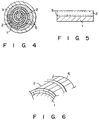
- Embodiments of oxide superconductors according to the present invention are sown in Figs. 1 to 4.
- Reference numerals 1 in Figs. 1 to 4 denote metal material layers; and 2, oxide superconductor layers.
- the metal material layers 1 and the oxide superconductor layers 2 are alternately laminated in a concentric shape, and the outermost layer is constituted by a metal coating layer 3.
- the metal material layer 1 and the oxide superconductor layer 2 are formed in a spiral form, and the metal coating layer 3 is used as the outermost layer.
- the concentric form shown in Fig. 1 includes the spiral form shown in Fig. 2.
- a plurality of superconductors shown in Fig. 1 or 2 can be bundled and wound around a metal material layer or an oxide superconductor layer, as shown in Fig. 3.
- a metal material layer or an oxide superconductor layer as shown in Fig. 3.
- four laminated structures each obtained by alternately laminating the metal material layers 1 and the oxide superconductor layers 2 in a rectangular form are bundled by one metal frame 4.
- the spiral laminated structure shown in Fig. 2 can be obtained by alternately laminating the metal sheets and the oxide superconductor sheets and winding the resultant laminated body.
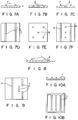
- Figs. 7A, 7B, and 7C The cross sections of metal sheets used in the method of the present invention are shown in Figs. 7A, 7B, and 7C, respectively, and the planar patterns thereof are shown in Figs. 7D, 7E, and 7F, respectively.
- Projections 7 and/or holes 8 are formed in the metal sheets to increase a contact area with the oxide semiconductor, thereby effectively performing heat dissipation.
- projections 7 of the metal sheet 1 are constituted by a plurality of linear projections 7, and an oxide superconductor 2 is applied between each two projections 7.
- the resultant metal sheet 1 with the oxide superconductor 2 is wound in a spiral shape to obtain a rod, or the metal sheets with the oxide superconductor are laminated to obtain a sheet-like body.
- the resultant structure is elongated in a direction of the linear projection 7.
- the oxide superconductor layers are separated from the projections 7, or the metal distribution density is increased to effectively suppress quenching and hyster
- Each linear projection formed on the metal sheet need not be continuous. As shown in the plan view of Fig. 9, projections 7 may be distributed as islands. When linear projections 7 are also formed along the sides of the metal sheet, as shown in the sectional and plan views of Figs. 10A and 10B, the oxide superconductor layers can be shielded from the outer atmosphere by using only the metal sheet without using a metal vessel.
- Fig. 4 is a sectional view showing an embodiment of an oxide superconductor in which metal particles are dispersed in the oxide superconductor layer.
- reference numerals 5 denote oxide superconductor layers in which metal particles are dispersed.
- a ring-like metal layer 3 is formed on the outer circumferential surface of the spiral body of the metal material and oxide superconductor layers 1 and 2.
- the oxide superconductor layers 5 containing the metal particles are arranged near the metal material layer 1.
- Each sectional shape of the superconductor of the present invention can be obtained by working such as rolling or drawing of the concentric superconductor.
- An example having a rectangular cross section is shown in Fig. 3.
- the lanky crystal is formed in the oxide superconductor layer in the current energization direction, the lanky crystal allow formation of a thinner wire.
- the superconductor body is used as a conductor such as a magnet, higher stability can be obtained.
- oxide superconductors are used in the oxide superconductors of the present invention.
- Metal materials for the metal material layers are nonreactive with oxide superconductors and are excellent in electrical conductivity and thermal conduction.
- the metal material are Ag, Ag-Pd, Ag-Au, Ag-Cu, Ag-Mg, Ag-Pt, Ag-Ir, Au, Au-Ni, Au-Cu, Au-Ag-Cu, Au-Pd-Ag, Au-Ir, Pt, Pt-Ir, Pt-Pd, Pd, Pd-Ni, Pd-Co, Ni-Cr, Ni-Cr-Co, Ni-Fe, Ni-Fe-Co, Fe-Cr, Fe, and Ni-Cr (SUS).
- the lanky crystal particle shape in the oxide superconductor layer according to the present invention is given such that a ratio (aspect ratio) of the length in the longitudinal direction of the superconductor to the length (width) in a direction perpendicular to the longitudinal direction is 10 or more and generally falls within the range of 50 to 1,000 because the C-axis orientation can be improved and a high Jc value can be obtained.
- the resultant oxide superconductor can be excellent in electrical conductivity and thermal conduction as a whole.
- an oxide superconductor of the present invention layers of an oxide superconductor or its precursor are alternately laminated with metal material layers by a desired number of times, and the laminated body is covered with the metal material.
- the laminated body with the coating is elongated as it is or into a desired shape.
- Predetermined heating and cooling are performed such that the laminated body is heated at a temperature to partially melt the oxide superconductor or its precursor or more and then cooled to recrystallize the oxide superconductor or its precursor.
- oxide superconductors used in the method of the present invention intermediate materials between source materials which can be converted into oxide superconductors and the oxide superconductors can be used as precursors in addition to the various oxide superconductors described above.
- the intermediate material is, e.g., a mixture, a coprecipitation mixture, or an oxygen deficient type composite oxides of oxide superconductor constituting elements, or an alloy of the above constituting elements. These precursors are heated in an atmosphere containing oxygen and are reacted into oxide superconductors.
- a method of forming the oxide superconductor or its precursor into a sheet can be a conventional method such as a doctor blade method, extrusion, or screen process printing. It is preferable to add a binder to the oxide superconductor or its precursor upon sheet formation because flexibility is imparted to the resultant sheet.
- the laminated body of sheets of the oxide superconductor or its precursor and the metal material sheets is heated to sinter the molded body, replenish oxygen to the sintered body, and adjust the crystal structure for the oxide superconductor, and to react the precursor into an oxide superconductor, to sinter the molded body, replenish oxygen to the sintered body, and adjust the crystal structures for the precursor.
- the oxide superconductor or its precursor is heated at a temperature to partially melt it or more because the lanky crystals are grown in the longitudinal direction during cooling and are oriented in the C-axis having a high conductivity.
- the laminated body is slowly moved in a furnace having a temperature gradient to facilitate lankiness of the crystals and C-axis orientation.
- the laminated body of the oxide superconductor sheets and the metal sheets is elongated by filling the laminated body into a metal vessel or covering the laminated body with a metal sheet because the oxide superconductor layers become more dense and are separated from the outer atmosphere to obtain a perfect moisture-proof structure, and are free from entrance of toxic substances.
- Any elongation method such as rolling, extrusion, groove rolling, swaging, or drawing can be applied.
- the oxide superconductor shown in Fig. 4 is manufactured as follows. As shown in Fig. 5, a sheet A of the oxide superconductor 5 containing metal particles, a sheet B of the oxide superconductor 2 which does not contain the metal particles, and another sheet A are laminated on the metal sheet 1, and the resultant body is wound in a spiral shape such that the metal sheet 1 becomes the outermost layer. The spiral body is filled in a metal pipe. The resultant structure is elongated in a desired manner, and predetermined heating is performed.
- FIG. 6 is a view showing part of a crystal structure of an oxide superconductor.
- An oxide superconductor layer 2 is formed on a metal material layer 1, and the oxide superconductor layer 2 is made of a plurality of lanky crystal particles 6 parallel to the axis of the superconductor.
- the particle boundary of the crystal particles has a pinning effect for restricting movement of a magnetic field. In a ferromagnetic magnet or AC energization, a high Jc can be stably obtained.
- a so-called Wind & React method can also be utilized wherein an elongated material of the laminated body is, for example, wound into a magnet coil and this coil is heated to obtain an oxide superconductor having good orientation.
- This method is very effective to form the oxide superconductor having poor workability into a magnet or the like.
- a high-strength, heat-resistant metal material can be embedded in the combined Ag or Ag alloy layer continuously in the longitudinal direction of the superconductor directly or through a noble metal layer.
- the Ag or Ag alloy is used as the metal material layer of the ceramic superconductor constituted by the ceramic superconductor layer and the metal material layer according to the present invention, and the high-strength, heat-resistant metal material can be continuously embedded in the Ag or Ag alloy layer in the longitudinal direction of the superconductor. Therefore, elongation deformation of the superconductor by a tension or the like can be prevented.
- the high-strength, heat-resistant metal material may be directly embedded in the Ag or Ag alloy layer.
- a noble metal layer is preferably coated on the high-strength, heat-resistant metal material, and the metal material with the noble metal layer is embedded into the Ag or Ag alloy layer to prevent oxidation of the metal material.
- the Ag or Ag alloy layer is used as the metal material layer combined with the ceramic superconductor due to the following reasons. Since Ag or an Ag alloy is excellent in oxygen permeability, a sufficient amount of oxygen is supplied to the ceramic superconductor during heating, thereby obtaining a high Jc. In addition, since Ag or an Ag alloy has a high heat conductivity, a quenching phenomenon, i.e., a thermal transition from superconductivity to normal conductivity, can be suppressed, and the energization amount can be increased.
- Any metal material combined with the ceramic superconductor can be used according to the present invention if it is excellent in oxygen permeability and thermal conduction.
- an Ag alloy such as Ag-Ir, Ag-Pd, or Ag-Au can be used.
- the superconductor shown in Fig. 11 is manufactured as follows. A ceramic superconductor material, and an Ag material or a high-strength, heat-resistant metal material are worked into rods or pipes, respectively. These rods or pipes are engaged with each other to obtain a composite billet. The composite billet is worked into a wire rod having a desired shape by the same elongation as described above. The resultant wire rod is heated at a temperature of, in most cases, 800 to 1,000°C to cause a reaction and sintering of the ceramic superconductor material into a ceramic superconductor, supply of oxygen to the sintered body, or adjustment of the crystal structure, thereby manufacturing a ceramic superconductor.
- a material which has high strength and cannot be melted or softened during heating in the subsequent process is used as the high-strength, heat-resistant metal material embedded in the Ag layer.
- examples of such a material are metals such as Fe, SUS, Ni, and W.
- the high-strength, heat-resistant metal material is preferably coated with a noble metal such as Au, Pt, Rd, or Pd by plating or vapor deposition, thereby preventing oxidation of the metal material.
- intermediate materials between source materials which can be converted into ceramic superconductors and the ceramic superconductors can be used as precursors in addition to the various ceramic superconductors described above.
- the intermediate material is, e.g., a mixture, a coprecipitation mixture, or an oxygen deficient type composite oxides of ceramic superconductor constituting elements, or an alloy of the above constituting elements. These precursors are heated in an atmosphere containing oxygen and are reacted into ceramic superconductors.
- the metal material is distributed in the form of a layer in the oxide superconductor layer in the oxide superconductor of the present invention, it is excellent in electrical conductivity and thermal conduction. Therefore, quenching and the hysteresis loss by AC energization can be suppressed.
- the crystal structure of the oxide superconductor layers partitioned by the metal material layers is constituted by crystal particles grown lanky in the longitudinal direction of the superconductor. Accordingly the number of particle boundaries accounting for energization resistance is small in the energization direction, and at least one particle boundary is contained in a direction perpendicular to the lanky crystal particles. Therefore, a uniform, high Jc can be obtained.
- the laminated body of the oxide superconductor and the metal is heated at a temperature to partially melt the oxide superconductor or more, and is then cooled to recrystallize the oxide superconductor such that crystallization of the molten oxide superconductor progresses to portions between the metal layers. Therefore, the crystal particles are grown lanky in the longitudinal direction and are oriented in the C-axis.
- Bi2O3, SrO, CaO, and CuO were mixed such that Bi : Sr : Ca : Cu was given as an atomic ratio of 2 : 2 : 1 : 2, the resultant powder was pre-burnt in air at 850°C for three hours, and the pre-burnt body was pulverized and classified to obtain a pre-burnt powder of Bi2Sr2CaCu2O x having an average particle size of 8/ ⁇ m.
- the heated body was then cooled, and the cooled body was filled in an Ag pipe having an inner diameter of 15 mm and a wall thickness of 2 mm.
- This Ag pipe was sealed in a vacuum, and subjected to hot isostatic pressing (HIP) at 500°C and 1,000 atm.
- HIP hot isostatic pressing
- the Ag pipe filled with the spiral body and subjected to HIP was formed into a 5.0-mm diameter wire material by swaging. This wire material was rolled into plate materials having thicknesses of 2.5 mm, 1.0 mm, and 0.5 mm.
- the plate materials were heated at 920°C for an hour, and the oxide superconductor layers were partially melted. Thereafter, the plate materials were gradually cooled to 860°C over three hours, heated at 860°C for eight hours, maintained at 820°C for six hours and then cooled. By this series of heating and cooling operations, plate-like oxide superconductors were manufactured.
- Plate-like oxide superconductors were manufactured following the same procedures as in Example 1 except that Ag pipes filled with spiral bodies and subjected to HIP were rolled without swaging to obtain plate members having thicknesses of 10 mm, 7.5 mm, and 5 mm.
- the green sheets containing the Ag powder were placed on the upper and lower surfaces of a 0.7-mm thick green sheet as in Example 1, and the resultant body was placed on a 0.7-mm thick Ag sheet.
- the resultant body was wound in a spiral form such that the Ag sheet faced outward, thereby obtaining a rod having a diameter of 15 mm.
- a plate-like oxide superconductor having a thickness of 1.0 mm was manufactured following the same procedures as in Example 1.
- a plate-like oxide superconductor having a thickness of 1.0 mm was manufactured following the same procedures as in Example 3 except that 0.15-mm thick green sheets placed on the upper and the lower surfaces of the 0.7-mm thick green sheet comprised green sheets without containing an Ag powder.
- Plate-like oxide superconductors were manufactured following the same procedures as in Examples 1 and 2 except that heating at 920°C for an hour for partial melting in heating of the plate materials and subsequent gradually cooling were omitted in Examples 1 and 2.
- the crystal particle shapes were represented by measuring lengths and widths of crystal particles.
- the oxide superconductor layers were heated at a temperature to partially melt the oxide superconductors during heating or more, the lanky crystal particles were oriented in the C-axis during cooling and were grown in the longitudinal direction of the superconductor.
- the particle boundaries which accounted for energization resistance in the direction perpendicular to the longitudinal direction were reduced.
- the particle boundaries in the longitudinal direction exhibited the pinning effect.
- the critical current density Jc is increased. This is considered to be attributable to the fact that a ratio of the length of the crystal particle to its width is increased when the thickness of the oxide superconductor layer is decreased, thereby increasing C-axis orientation of the crystal particles.
- a higher Jc is obtained than the sample (No. 8) in which the Ag powder is not distributed. This is because the thermal conduction and electrical conductivity from the oxide superconductor layer to the metal material layer are improved due to the presence of the Ag powder.
- the oxide superconductor layer heated by a low heating temperature was not partially melted, and the crystal structure of the oxide superconductor was constituted by isometric crystals.
- the particle boundaries in a direction perpendicular to the longitudinal direction were increased, and the crystal particle were oriented randomly. Therefore, the critical current densities Jc became low.
- Green sheets as in Example 1 were placed on 0.7-mm thick Ag sheets, respectively, and the laminated body were wound in spiral form such that the Ag sheet faces outward.
- the spiral bodies were subjected to HIP as in Example 1.
- the HIP-treated bodies were heated at 920°C for an hour under the same conditions as in Example 1 or in air to partially melt the oxide superconductor layers.
- the bodies were then moved at a rate of 1 cm/five hours in a furnace having a temperature gradient and cooled from 920°C to 820°C at a rate of 40°C/cm.
- Crystal orientation F of the oxide superconductors thus obtained were measured following the same procedures as in Example 1. Results are summarized in Table 2 together with the manufacturing conditions. Table 2 No. No. of laminating Green Sheets Thickness of Superconductor Layer (mm) Temperature Gradient in Furance during Cooling F % 1 1 0.6 No 40 2 2 0.8 " 15 3 4 1.7 " 5> 4 4 1.7 Yes 35
- the pre-burnt body was filled in an Ag vessel having inner dimensions of 100 ⁇ 100 ⁇ 10 mm and a wall thickness of 2 mm and was sealed in a vacuum.
- the sealed vessel was subjected to HIP in an Ar atmosphere at 600°C and 1,000 atm.
- the HIP-treated vessel was rolled to have a thickness of 0.8 mm. The rolled material was heated in an O2 flow at 900°C for six hours and was cooled to room temperature at a rate of 3°C/min to manufacture a sheet-like oxide superconductor.
- the Ag sheet was wound in a spiral form so that the linear projections were parallel to the longitudinal direction to obtain a 25-mm diameter rod.
- This rod was filled in an Ag pipe having an inner diameter of 25 mm and a wall thickness of 2 mm.
- the filled Ag pipe was heated to 800°C at a rate of 5°C/min and was then subjected to drying, binder elimination, and pre-sintering.
- the Ag pipe was sealed in a vacuum and was subjected to HIP in an Ar atmosphere at 500°C and 1,000 atm.
- the Ag pipe with the contents was swaged by a swager to a wire rod having a diameter of 5 mm and then drawn into a wire rod having a diameter of 2 mm.
- This wire rod was rolled while twisting it at a pitch of 1/150 to prepare a rolled material having a thickness of 0.8 mm.
- the rolled material was heated in air at 840°C for 12 hours and was then cooled to room temperature at a rate of 3°C/min.
- the rolled material having a thickness of 0.8 mm was kept heated at 900°C for half an hour and gradually cooled to 840°C over 30 minutes prior to the above heating operation, and thereafter, the above-mentioned heating operation was performed. Heating was performed by either method to obtain a tape-like oxide superconductor.
- Oxide superconductors were manufactured following the same procedures as in Example 6 except that the Ag vessels filled with the laminated bodies were heated without rolling after the HIP treatment.
- Oxide superconductors were manufactured following the same procedures as in Example 6 except that the Ag vessels filled with the spiral rods were heated without working after the HIP treatment.
- Oxide superconductors were manufactured following the same procedures as in Example 8 except that the Ag vessels filled with the spiral rods were pre-sintered and subjected to HIP, and heated without working.
- Magnetic shield effects of the sheet-like oxide superconductors were measured.
- the magnet shield effect was measured such that an electromagnet which generated a magnetic field having a strength of 20 gauss was shielded by the above mentioned superconductor cooled to 77K, and an external magnetic force was measured by a gaussmeter.
- the samples of the examples (sample Nos. 1 to 5) of the method of the present invention have larger Jc values and higher shield effects as compared with the samples of the method of the comparative examples (sample Nos. 6 to 8). This difference is caused depending upon whether the elongation step of the laminated body is performed, as is apparent upon comparison of sample Nos. 1, 4, and 5 of the present invention with sample Nos. 6, 7, and 8 of the comparative examples.
- the oxide superconductor layer of the method of the present invention had higher crystal orientation and became dense since elongation was performed.
- the samples (Nos. 2 and 3) having the projections on the metal sheets have larger Jc values than the samples (Nos. 4 and 5) having no projections because the metal was finely distributed and quenching and the hysteresis loss were effectively suppressed.
- the samples (Nos. 3 and 5) subjected to preheating prior to heating have larger Jc values than the samples (Nos. 2 and 4) subjected to heating without preheating. This is because the oxide superconductor was partially melted by preheating and crystal orientation was increased.
- the Ag powder was mixed in the oxide superconductor powder in Example 6 in order to increase adhesion strength between the oxide superconductor layer and the metal layer, to increase heat conductivity, and to promote supply of oxygen during heating, thereby increasing Jc values and the like.
- the crystal orientation of sample Nos. 2 to 5 is higher than that of sample No. 1 due to different working methods. That is, drawing contributed to improve the crystal orientation as compared with rolling.
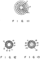
- An oxide superconductor wire 10 shown in Fig. 12 comprises a plurality of stabilizing metal layers 11, 12, 13, and 14 having ring-like sectional shapes of different diameters, and a plurality of oxide superconductor layers 15, 16, and 17 having ring-like sectional shapes of different diameters.
- the stabilizing metal layers 11 to 14 and the oxide superconductor layers 15 to 17 were alternately laminated in an order of the stabilizing metal layer 11, the oxide superconductor layer 15, the stabilizing metal layer 12, the oxide superconductor layer 16, the stabilizing metal layer 13, the oxide superconductor layer 17, and the stabilizing metal layer 14 from the center to the outer surface of the oxide superconductor wire 10.
- An oxide superconductor wire 20 shown in Fig. 13 has the same basic structure as the oxide superconductor wire 10 in Fig. 12.
- the oxide superconductor wire 20 comprises a plurality of stabilizing metal layers 21, 22, 23, and 24 and a plurality of oxide superconductor layers 25, 26, and 27, which are alternately laminated in the radial direction.
- the stabilizing metal layer 21 at the core comprises a rod, and other stabilizing metal layers 22 to 24 and the oxide superconductor layers 25 to 27 are ring-like sectional shapes.
- the stabilizing metal layers 11 to 14 and 21 to 24 are made of, e.g., silver or a nickel-based alloy.
- the oxide superconductor layers 15 to 17, and 25 to 27 are made of a known composition such as Lu-Ba-Cu-O or Bi-Sr-Ca-Cu-O.
- the oxide superconductor layers 15 to 17 and 25 to 27 are constituted by an aggregate of an oxide powder having the longitudinal direction as an a-b plane and the direction of thickness as the c-axis, critical current densities (Jc) of the oxide superconductor layers 15 to 17 and 25 to 27 can be increased.
- each of the oxide superconductor layers 15 to 17 and 25 to 27 is 200 ⁇ m or less and is preferably as small as possible.
- each of the stabilizing metal layers 11 to 14 and 21 to 24 is as small as possible so as to minimize the outer diameter of each of the superconductor wires 10 and 20. When the thickness is excessively small, the stabilizing function inherent to this metal layer is impaired.
- each of the stabilizing metal layers 11 to 14 and 21 to 24 is preferably set to be several times that of each of the oxide superconductor layers 15 to 17 and 25 to 27.
- the number of oxide superconductor layers in each of the oxide superconductor wires 10 and 20 is arbitrarily set to be two or more, and the number of stabilizing metal layers is set accordingly.
- the hollow core portion can serve as a refrigerant flow path to improve cooling capacity, thereby obtaining a more desirable oxide superconductor wire.
- Fig. 15 shows tubular stabilizing metal materials 30a, 31, 32, 33, and 34 to which an oxide powder is applied, and a rod-like stabilizing metal material 30b.
- the stabilizing metal materials 30a, 30b, 31, 32, 33, and 34 are made of sliver or a nickel-based alloy.
- the stabilizing metal materials 30a, 31, 32, 33, and 34 are used, and an oxide powder is applied to the outer surface of the stabilizing material 30a, one or both of the inner and outer surfaces of the stabilizing metal materials 31, 32, and 33, and the inner surface of the stabilizing metal material 34.
- a predetermined oxide powder is applied to the outer surfaces of the stabilizing metal materials 30a, 31, 32, 33, and 34, and these stabilizing metal materials 30a, 31, 32, 33, and 34 are combined together.
- the surface area of the resultant composite material is reduced by a surface area reducing means such as swaging or rolling.
- the area-reduced composite material is heated in an oxygen atmosphere, thereby obtaining the oxide superconductor wire 10 shown in Fig. 12.
- the oxide superconductor wire 20 shown in Fig. 13 can be manufactured following the same procedures as described above except that the rod-like stabilizing metal material 30b is used in place of the tubular stabilizing metal material 30a.
- Oxide powders including a Y2O3,BaCO3 and CuO powder were weighed and mixed such that Y : Ba : Cu was given as a molar ratio of 1 : 2 : 3.
- the resultant powder mixture was pre-burnt in an oxygen atmosphere at 920°C for 20 hours.
- the pre-burnt mixture was heated and melted at 1,300°C and solidified at a cooling rate of 10°C/sec to obtain a plate having a thickness of 1 mm.
- the plate was heated in an oxygen atmosphere at 950°C for 50 hours and pulverized into an oxide powder having a size of 4 ⁇ m in an automatic mortar.
- the resultant oxide powder was kneaded with a binder, and the kneaded material was applied to the outer surfaces of the silver stabilizing metal materials 30a, 31, 32, and 33 (Table 4) to a thickness of 20 ⁇ m.
- the binder contained in the kneaded material applied to the stabilizing metal materials 30a, 31, 32, and 33 was eliminated.
- the stabilizing metal materials 30a, 31, 32, and 33 which carried the predetermined oxide powder and the silver stabilizing metal material 34 without an oxide powder were combined in a concentric form, and the surface area of the resultant structure was reduced by cold-rolling to obtain a composite wire having an outer diameter of 2 mm.
- the composite wire was heated in an oxygen atmosphere at 830° for 20 hours to obtain the oxide superconductor wire 10.
- An oxide superconductor wire 20 was manufactured following the same procedures as in Example 9 except that the stabilizing metal material 30b shown in Table 4 was used in place of the stabilizing metal material 30a.
- An oxide superconductor wire 10 was manufactured following the same procedures as in Example 9 except that the oxide powder was replaced with a pre-burnt powder having a particle size of 5 ⁇ m.
- a pre-burnt powder as in Example 11 was used as an oxide powder for the superconductor, and a silver pipe 41 having an outer diameter of 20 mm and an inner diameter of 15 mm was used as a metal sheath, as shown in Fig. 16.
- the pipe 41 filled with a pre-burnt powder 42 was worked by a surface area reducing means to obtain a superconductor wire 40 having an outer diameter of 0.5 mm, as shown in Fig. 16.
- the bending characteristics were measured such that each oxide superconductor wire was bent with a radius of curvature which was 50 times the outer diameter to determine whether the oxide superconductor was damaged. If the oxide superconductor was not damaged, it was represented by a circle; and if the oxide superconductor was damaged, it was represented by a cross.
- the samples of examples 9 to 11 of the present invention have excellent bending characteristics, are free from damage, and larger Jc values than the sample of Comparative Example 5.
- the samples of Examples 9 and 10 have excellent properties.
- the metal is finely distributed in the oxide superconductor in the form of a layer.
- the oxide superconductor is excellent in thermal and electrical conductivities.
- the oxide superconductor layer present between the metal layers is constituted by lanky crystal oriented in the C-axis.
- the oxide superconductor layer has particle boundaries which exhibit the pinning effect, so that the oxide superconductor has excellent superconductive characteristics such as a higher critical current density (Jc) and excellent mechanical characteristics (bending characteristics).
- Jc critical current density
- bending characteristics bending characteristics
- a laminated body of an oxide superconductor or its precursor and a metal is heated at a temperature to partially melt the oxide superconductor or its precursor or more, thereby easily manufacturing the superconductor described above and providing remarkable industrial effect.
- a metal sheet is continuously distributed in an oxide superconductor layer, and this structure is elongated. Therefore, the oxide superconductor layer becomes dense and crystal orientation can be increased.
- the metal sheet serves as a thermal and electrical conductor in the oxide superconductor, quenching and hysteresis loss can be suppressed to increase a Jc value and improve the shield effect, thereby rationally manufacturing oxide superconductors having excellent properties, and providing a remarkable industrial effect.
Abstract
Description
- The present invention relates to an oxide superconductor used in a transmission and distribution wire, a power cable, an equipment lead wire, a magnet wire, and a magnetic shield and a method of manufacturing the same and, more particularly, to an oxide superconductor capable of supplying a large current with zero resistance or small alternating-current loss.
- An intermetallic compound such as NbTi, Nb₃Sn, Nb₃Aℓ, or V₃Ga and a metal such as Nb or Pb are used as superconductive magnets, magnetic shields, coaxial cables, and cavities by utilizing an ultra low-temperature refrigerant such as liquid helium. These metallic materials, however, are limited as resources. In addition, helium is used to increase cost, which limits the range of practical applications.
- To the contrary, some substances which can be rendered superconductive at low critical temperatures (Tc) by inexpensive refrigerants have been found, and extensive studies on practical use of such substances in a variety of applications have been actively made.
- As the high Tc materials described above, La2-xBaxCu0₄ and La2-xSrxCuO₄ oxide superconductors have critical temperatures of 30 to 45K; a Y(Dy,Er,Ho)Ba₂Cu3O₇₋δ oxide superconductor has a critical temperature of up to 95K; Bi-Sr-Ca-Cu-O based oxide superconductors such as Bi₂Sr₂CaCu₂O₈ and Bi₂Sr₂Ca₂Cu₃O₁₀ oxide superconductors have critical temperatures of 80 to 110K; and Tℓ-Ba-Ca-Cu-O based oxide superconductors such as Tl₂Ba₂CaCu₂O₈, Tℓ₂Ba₂Ca₂Cu₃O₁₀ and TℓBa₂Ca₂Cu₇O8.5 oxide superconductors have critical temperatures of 90 to 125K. These oxide superconductors are manufactured as follows. A powder of each superconductor is kneaded with an organic binder to obtain a paste, and the paste is directly extrusion molded or screen-printed. Alternatively, the powder of each superconductor is filled in an Ag pipe or the like, and the pipe is elongated to obtain a conductor having a desired shape.
- In a superconductor, a metal stabilizing material is combined with a superconductor molded body to cope with a so-called quench phenomenon in which a superconductive state is lost. For the same purpose as in the oxide superconductor, it is proposed to combine a metal stabilizing material with an oxide superconductor. When the superconductive state is lost, the oxide superconductor becomes an insulator, and it is difficult to conduct heat or electric power to the metal stabilizing material. For this reason, a quench phenomenon more easily occurs. In particular, in alternating-current energization, heat may often be generated by a hysteresis loss. It is very important to appropriately provide a countermeasure against the quench phenomenon of the oxide superconductor.
- An oxide superconductor is generally brittle and its crystal has a laminar structure subjected to cleavage. The oxide superconductors tend to crack in installation works. In addition, when an oxide superconductor is used for a magnet, a Lorentz's force acts on the oxide superconductor to crack an oxide superconductor layer. As a result, a critical current density (Jc) is undesirably degraded. Furthermore, since the oxide superconductor has a laminar perovskite crystal structure, crystal anisotropy is strong, and a current flows in a direction parallel to the a-b plane. In order to obtain a high critical current density (Jc), the crystal must be oriented such that its C-axis is perpendicular to a current energization direction. However, since the crystal of the oxide superconductor thus manufactured tend to be oriented randomly, a sufficiently high critical current density Jc cannot be obtained.
- The present invention has been made as a result of extensive studies in consideration of the above situation, and has as its object to provide an oxide superconductor having excellent electromagnetic stability such as a high Jc and high mechanical strength and a method of manufacturing the same.
- According to the present invention, there is provided an oxide superconductor in which oxide superconductor layer and metal material layers are alternately laminated by a plurality of times.
- The oxide superconductor having the above structure according to the present invention has a multilayered structure in which the oxide superconductor layers and the metal material layers are alternately laminated. Therefore, both electromagnetic stability and mechanical strength which are indispensable factors of the superconductor can be obtained.
- According to an embodiment of the present invention, the metal material layers are discontinuously laminated in the circumferential direction of the superconductor because the stabilizing metal layers of the laminated body of the present invention serve as a barrier when the structure is used as a superconductor such as a power cable. Therefore, when the outer superconductor layer is not rendered superconductive, the current does not flow into the inner superconductor layer through the metal material interlayer.
- In order to uniformly flow a current in each superconductor layer of the multilayered structure, the metal material layers can be discontinuous in the circumferential direction of the conductor.
- For this purpose, the metal material layer may have a porous or net-like structure. Alternatively, a metal material sheet having a small width may be wound around the superconductor in a helical shape so as to partially expose the underlying superconductor layer.
- This invention can be more fully understood from the following detailed description when taken in conjunction with the accompanying drawings, in which:
- Figs. 1 to 3 are sectional views showing examples of oxide superconductors according to the present invention;
- Figs. 4 and 5 are a sectional view of an oxide superconductor in which a metal powder (particles) is dispersed in an oxide superconductor layer, and a view for explaining a method of manufacturing it, respectively;
- Fig. 6 is a view for explaining a crystal structure of an oxide superconductor layer of an oxide superconductor according to the present invention;
- Figs. 7A to 7C are sectional views showing metal sheets used in the present invention;
- Figs. 7D to 7F are plan views showing the metal sheets shown in Figs. 7A to 7C, respectively;
- Fig. 8 is a sectional view showing a state wherein an oxide superconductor layer is laminated on a metal sheet;
- Fig. 9 is a plan view showing still another metal sheet used in the present invention;
- Figs. 10A and 10B are a sectional view and a plan view, respectively, showing still another metal sheet used in the present invention;
- Fig. 11 is a sectional view showing a superconductor in which a high-strength, heat-resistant metal material is combined with an oxide superconductor according to the present invention;
- Figs. 12 and 13 are sectional views showing other examples of oxide superconductor cables according to the present invention;
- Figs. 14A and 14B are a view for explaining the enlarged main part of an oxide superconductor cable according to the present invention, and a view for explaining the directions of a-, b- and c-axis of the oxide superconductor cable, respectively.
- Fig. 15 is a sectional view showing various types of stabilizing metal materials used in the method of manufacturing oxide superconductor cables according to the present invention; and
- Fig. 16 is a sectional view showing a conventional oxide superconductor cable.
- Embodiments of oxide superconductors according to the present invention are sown in Figs. 1 to 4. Reference numerals 1 in Figs. 1 to 4 denote metal material layers; and 2, oxide superconductor layers.
- In the oxide superconductor shown in Fig. 1, the metal material layers 1 and the
oxide superconductor layers 2 are alternately laminated in a concentric shape, and the outermost layer is constituted by ametal coating layer 3. In the oxide superconductor shown in Fig. 2, the metal material layer 1 and theoxide superconductor layer 2 are formed in a spiral form, and themetal coating layer 3 is used as the outermost layer. The concentric form shown in Fig. 1 includes the spiral form shown in Fig. 2. - According to the present invention, a plurality of superconductors shown in Fig. 1 or 2 can be bundled and wound around a metal material layer or an oxide superconductor layer, as shown in Fig. 3. In the oxide superconductor shown in Fig. 3, four laminated structures each obtained by alternately laminating the metal material layers 1 and the
oxide superconductor layers 2 in a rectangular form are bundled by onemetal frame 4. - The spiral laminated structure shown in Fig. 2 can be obtained by alternately laminating the metal sheets and the oxide superconductor sheets and winding the resultant laminated body.
- The cross sections of metal sheets used in the method of the present invention are shown in Figs. 7A, 7B, and 7C, respectively, and the planar patterns thereof are shown in Figs. 7D, 7E, and 7F, respectively.
Projections 7 and/orholes 8 are formed in the metal sheets to increase a contact area with the oxide semiconductor, thereby effectively performing heat dissipation. As shown in Fig. 8,projections 7 of the metal sheet 1 are constituted by a plurality oflinear projections 7, and anoxide superconductor 2 is applied between each twoprojections 7. The resultant metal sheet 1 with theoxide superconductor 2 is wound in a spiral shape to obtain a rod, or the metal sheets with the oxide superconductor are laminated to obtain a sheet-like body. The resultant structure is elongated in a direction of thelinear projection 7. Then, the oxide superconductor layers are separated from theprojections 7, or the metal distribution density is increased to effectively suppress quenching and hysteresis loss. - Each linear projection formed on the metal sheet need not be continuous. As shown in the plan view of Fig. 9,
projections 7 may be distributed as islands. Whenlinear projections 7 are also formed along the sides of the metal sheet, as shown in the sectional and plan views of Figs. 10A and 10B, the oxide superconductor layers can be shielded from the outer atmosphere by using only the metal sheet without using a metal vessel. - Fig. 4 is a sectional view showing an embodiment of an oxide superconductor in which metal particles are dispersed in the oxide superconductor layer. Referring to Fig. 4,
reference numerals 5 denote oxide superconductor layers in which metal particles are dispersed. A ring-like metal layer 3 is formed on the outer circumferential surface of the spiral body of the metal material andoxide superconductor layers 1 and 2. Theoxide superconductor layers 5 containing the metal particles are arranged near the metal material layer 1. - Each sectional shape of the superconductor of the present invention can be obtained by working such as rolling or drawing of the concentric superconductor. An example having a rectangular cross section is shown in Fig. 3.
- In each oxide superconductor layer described above, lanky crystal particles of which longitudinal direction are oriented in the longitudinal direction of the superconductor and includes at least one particle boundary in a direction perpendicular to the longitudinal direction.
- Since the lanky crystal is formed in the oxide superconductor layer in the current energization direction, the lanky crystal allow formation of a thinner wire. When the superconductor body is used as a conductor such as a magnet, higher stability can be obtained.
- Various types of oxide superconductors are used in the oxide superconductors of the present invention. Metal materials for the metal material layers are nonreactive with oxide superconductors and are excellent in electrical conductivity and thermal conduction. Examples of the metal material are Ag, Ag-Pd, Ag-Au, Ag-Cu, Ag-Mg, Ag-Pt, Ag-Ir, Au, Au-Ni, Au-Cu, Au-Ag-Cu, Au-Pd-Ag, Au-Ir, Pt, Pt-Ir, Pt-Pd, Pd, Pd-Ni, Pd-Co, Ni-Cr, Ni-Cr-Co, Ni-Fe, Ni-Fe-Co, Fe-Cr, Fe, and Ni-Cr (SUS). The lanky crystal particle shape in the oxide superconductor layer according to the present invention is given such that a ratio (aspect ratio) of the length in the longitudinal direction of the superconductor to the length (width) in a direction perpendicular to the longitudinal direction is 10 or more and generally falls within the range of 50 to 1,000 because the C-axis orientation can be improved and a high Jc value can be obtained.
- When the metal particles are dispersed at least in an oxide superconductor layer portion adjacent to the metal material layer, and the thickness of each oxide superconductor layer is reduced to 1 mm or less and preferably 0.1 mm or less, the resultant oxide superconductor can be excellent in electrical conductivity and thermal conduction as a whole.
- According to a method of manufacturing an oxide superconductor of the present invention, layers of an oxide superconductor or its precursor are alternately laminated with metal material layers by a desired number of times, and the laminated body is covered with the metal material. The laminated body with the coating is elongated as it is or into a desired shape. Predetermined heating and cooling are performed such that the laminated body is heated at a temperature to partially melt the oxide superconductor or its precursor or more and then cooled to recrystallize the oxide superconductor or its precursor.
- As the oxide superconductors used in the method of the present invention, intermediate materials between source materials which can be converted into oxide superconductors and the oxide superconductors can be used as precursors in addition to the various oxide superconductors described above. The intermediate material is, e.g., a mixture, a coprecipitation mixture, or an oxygen deficient type composite oxides of oxide superconductor constituting elements, or an alloy of the above constituting elements. These precursors are heated in an atmosphere containing oxygen and are reacted into oxide superconductors.
- In this method of the present invention, in order to alternately laminate an oxide superconductor or its precursor with the metal material by a desired number of times, it is easy to form sheets of the superconductor or its precursor, and the metal material sheets, and to alternately laminate these sheets to obtain a laminated structure. A method of forming the oxide superconductor or its precursor into a sheet can be a conventional method such as a doctor blade method, extrusion, or screen process printing. It is preferable to add a binder to the oxide superconductor or its precursor upon sheet formation because flexibility is imparted to the resultant sheet.
- According to the method of the present invention, the laminated body of sheets of the oxide superconductor or its precursor and the metal material sheets is heated to sinter the molded body, replenish oxygen to the sintered body, and adjust the crystal structure for the oxide superconductor, and to react the precursor into an oxide superconductor, to sinter the molded body, replenish oxygen to the sintered body, and adjust the crystal structures for the precursor. The oxide superconductor or its precursor is heated at a temperature to partially melt it or more because the lanky crystals are grown in the longitudinal direction during cooling and are oriented in the C-axis having a high conductivity. The laminated body is slowly moved in a furnace having a temperature gradient to facilitate lankiness of the crystals and C-axis orientation.
- According to the method of the present invention, the laminated body of the oxide superconductor sheets and the metal sheets is elongated by filling the laminated body into a metal vessel or covering the laminated body with a metal sheet because the oxide superconductor layers become more dense and are separated from the outer atmosphere to obtain a perfect moisture-proof structure, and are free from entrance of toxic substances. Any elongation method such as rolling, extrusion, groove rolling, swaging, or drawing can be applied.
- The oxide superconductor shown in Fig. 4 is manufactured as follows. As shown in Fig. 5, a sheet A of the
oxide superconductor 5 containing metal particles, a sheet B of theoxide superconductor 2 which does not contain the metal particles, and another sheet A are laminated on the metal sheet 1, and the resultant body is wound in a spiral shape such that the metal sheet 1 becomes the outermost layer. The spiral body is filled in a metal pipe. The resultant structure is elongated in a desired manner, and predetermined heating is performed. - A crystal structure of an oxide superconductor layer of an oxide superconductor of the present invention will be described with reference to Fig. 6. Fig. 6 is a view showing part of a crystal structure of an oxide superconductor.
- An
oxide superconductor layer 2 is formed on a metal material layer 1, and theoxide superconductor layer 2 is made of a plurality oflanky crystal particles 6 parallel to the axis of the superconductor. The particle boundary of the crystal particles has a pinning effect for restricting movement of a magnetic field. In a ferromagnetic magnet or AC energization, a high Jc can be stably obtained. - According to the method of the present invention, a so-called Wind & React method can also be utilized wherein an elongated material of the laminated body is, for example, wound into a magnet coil and this coil is heated to obtain an oxide superconductor having good orientation. This method is very effective to form the oxide superconductor having poor workability into a magnet or the like.
- In a ceramic superconductor in which an Ag layer or an Ag alloy layer is combined with a ceramic superconductor layer, a high-strength, heat-resistant metal material can be embedded in the combined Ag or Ag alloy layer continuously in the longitudinal direction of the superconductor directly or through a noble metal layer.
- The Ag or Ag alloy is used as the metal material layer of the ceramic superconductor constituted by the ceramic superconductor layer and the metal material layer according to the present invention, and the high-strength, heat-resistant metal material can be continuously embedded in the Ag or Ag alloy layer in the longitudinal direction of the superconductor. Therefore, elongation deformation of the superconductor by a tension or the like can be prevented. The high-strength, heat-resistant metal material may be directly embedded in the Ag or Ag alloy layer. However, a noble metal layer is preferably coated on the high-strength, heat-resistant metal material, and the metal material with the noble metal layer is embedded into the Ag or Ag alloy layer to prevent oxidation of the metal material.
- As described above, the Ag or Ag alloy layer is used as the metal material layer combined with the ceramic superconductor due to the following reasons. Since Ag or an Ag alloy is excellent in oxygen permeability, a sufficient amount of oxygen is supplied to the ceramic superconductor during heating, thereby obtaining a high Jc. In addition, since Ag or an Ag alloy has a high heat conductivity, a quenching phenomenon, i.e., a thermal transition from superconductivity to normal conductivity, can be suppressed, and the energization amount can be increased.
- Any metal material combined with the ceramic superconductor can be used according to the present invention if it is excellent in oxygen permeability and thermal conduction. For example, an Ag alloy such as Ag-Ir, Ag-Pd, or Ag-Au can be used.
- In a superconductor shown in Fig. 11, an Ag layer 1, a
ceramic superconductor layer 2, and a high-strength, heat-resistant metal material 9 are combined in a concentric manner. - The superconductor shown in Fig. 11 is manufactured as follows. A ceramic superconductor material, and an Ag material or a high-strength, heat-resistant metal material are worked into rods or pipes, respectively. These rods or pipes are engaged with each other to obtain a composite billet. The composite billet is worked into a wire rod having a desired shape by the same elongation as described above. The resultant wire rod is heated at a temperature of, in most cases, 800 to 1,000°C to cause a reaction and sintering of the ceramic superconductor material into a ceramic superconductor, supply of oxygen to the sintered body, or adjustment of the crystal structure, thereby manufacturing a ceramic superconductor.
- A material which has high strength and cannot be melted or softened during heating in the subsequent process is used as the high-strength, heat-resistant metal material embedded in the Ag layer. Examples of such a material are metals such as Fe, SUS, Ni, and W. The high-strength, heat-resistant metal material is preferably coated with a noble metal such as Au, Pt, Rd, or Pd by plating or vapor deposition, thereby preventing oxidation of the metal material.
- As the ceramic superconductor materials used in the method of the present invention, intermediate materials between source materials which can be converted into ceramic superconductors and the ceramic superconductors can be used as precursors in addition to the various ceramic superconductors described above. The intermediate material is, e.g., a mixture, a coprecipitation mixture, or an oxygen deficient type composite oxides of ceramic superconductor constituting elements, or an alloy of the above constituting elements. These precursors are heated in an atmosphere containing oxygen and are reacted into ceramic superconductors.
- Since the metal material is distributed in the form of a layer in the oxide superconductor layer in the oxide superconductor of the present invention, it is excellent in electrical conductivity and thermal conduction. Therefore, quenching and the hysteresis loss by AC energization can be suppressed.
- The crystal structure of the oxide superconductor layers partitioned by the metal material layers is constituted by crystal particles grown lanky in the longitudinal direction of the superconductor. Accordingly the number of particle boundaries accounting for energization resistance is small in the energization direction, and at least one particle boundary is contained in a direction perpendicular to the lanky crystal particles. Therefore, a uniform, high Jc can be obtained.
- In the method of manufacturing the above oxide superconductor according to the present invention, the laminated body of the oxide superconductor and the metal is heated at a temperature to partially melt the oxide superconductor or more, and is then cooled to recrystallize the oxide superconductor such that crystallization of the molten oxide superconductor progresses to portions between the metal layers. Therefore, the crystal particles are grown lanky in the longitudinal direction and are oriented in the C-axis.
- The present invention will be described in detail by way of its examples.
- Bi₂O₃, SrO, CaO, and CuO were mixed such that Bi : Sr : Ca : Cu was given as an atomic ratio of 2 : 2 : 1 : 2, the resultant powder was pre-burnt in air at 850°C for three hours, and the pre-burnt body was pulverized and classified to obtain a pre-burnt powder of Bi₂Sr₂CaCu₂Ox having an average particle size of 8/µm.
- Ten vol% of methyl cellulose and 10 vol% of methyl cellosolve as binders were mixed with the pre-burnt powder, and the resultant mixture was kneaded by a roll. From the kneaded mass, a tape-like green sheet having a thickness of 0.7 mm was formed by a doctor blade method. This green sheet was placed on an Ag sheet having a thickness of 0.7 mm, and the laminated body was wound in a spiral form such that the Ag sheet faces outward, thereby obtaining a rod having a diameter of 15 mm. The rod was heated to 150°C to eliminate volatile components such as binders, and then heated in air at 800°C for an hour. The heated body was then cooled, and the cooled body was filled in an Ag pipe having an inner diameter of 15 mm and a wall thickness of 2 mm. This Ag pipe was sealed in a vacuum, and subjected to hot isostatic pressing (HIP) at 500°C and 1,000 atm. The Ag pipe filled with the spiral body and subjected to HIP was formed into a 5.0-mm diameter wire material by swaging. This wire material was rolled into plate materials having thicknesses of 2.5 mm, 1.0 mm, and 0.5 mm.
- The plate materials were heated at 920°C for an hour, and the oxide superconductor layers were partially melted. Thereafter, the plate materials were gradually cooled to 860°C over three hours, heated at 860°C for eight hours, maintained at 820°C for six hours and then cooled. By this series of heating and cooling operations, plate-like oxide superconductors were manufactured.
- Plate-like oxide superconductors were manufactured following the same procedures as in Example 1 except that Ag pipes filled with spiral bodies and subjected to HIP were rolled without swaging to obtain plate members having thicknesses of 10 mm, 7.5 mm, and 5 mm.
- Fifteen % of an Ag powder (particles) having a diameter of 1 µm were mixed with a pre-burnt Bi₂Sr₂CaCu₂Ox powder, binders as in Example 1 were mixed with the resultant powder mixture, and a green sheet having a thickness of 0.15 mm was formed by a doctor blade method.
- The green sheets containing the Ag powder were placed on the upper and lower surfaces of a 0.7-mm thick green sheet as in Example 1, and the resultant body was placed on a 0.7-mm thick Ag sheet. The resultant body was wound in a spiral form such that the Ag sheet faced outward, thereby obtaining a rod having a diameter of 15 mm. Thereafter, from the rod, a plate-like oxide superconductor having a thickness of 1.0 mm was manufactured following the same procedures as in Example 1.
- A plate-like oxide superconductor having a thickness of 1.0 mm was manufactured following the same procedures as in Example 3 except that 0.15-mm thick green sheets placed on the upper and the lower surfaces of the 0.7-mm thick green sheet comprised green sheets without containing an Ag powder.
- Plate-like oxide superconductors were manufactured following the same procedures as in Examples 1 and 2 except that heating at 920°C for an hour for partial melting in heating of the plate materials and subsequent gradually cooling were omitted in Examples 1 and 2.
- Crystal particle shapes, Jc values, and crystal orientations of the oxide superconductor layers of the oxide superconductors thus obtained were measured.
- The critical current densities Jc were measured by a four-terminal method at 77K using 1 µV/cm as a standard. Crystal orientation F was calculated by the following equation such that an internal oxide superconductor layer was exposed and irradiated with X-rays, and diffraction intensities of the exposed portions were substituted:

where
Po is the diffraction intensity ratio of the oxide superconductor layer
Poo is the diffraction intensity ratio of the uniformly mixed oxide superconductor powder

where (hkℓ) is the intensity of the (hkℓ) diffraction beam. The crystal particle shapes were represented by measuring lengths and widths of crystal particles. - Results are summarized in Table 1 below together with the manufacturing conditions.

- As is apparent from Table 1, the examples (sample Nos. 1 to 8) of the present invention had higher critical current densities Jc than comparative examples (sample Nos. 9 to 14).
- In the samples of the examples of the present invention, since the oxide superconductor layers were heated at a temperature to partially melt the oxide superconductors during heating or more, the lanky crystal particles were oriented in the C-axis during cooling and were grown in the longitudinal direction of the superconductor. The particle boundaries which accounted for energization resistance in the direction perpendicular to the longitudinal direction were reduced. In addition, the particle boundaries in the longitudinal direction exhibited the pinning effect.
- In the samples of the examples of the present invention, when the thickness of the oxide superconductor layer is decreased, the critical current density Jc is increased. This is considered to be attributable to the fact that a ratio of the length of the crystal particle to its width is increased when the thickness of the oxide superconductor layer is decreased, thereby increasing C-axis orientation of the crystal particles. In addition, in the sample (No. 7) in which the Ag powder (particles) is distributed in the oxide superconductor layer portion near the metal material layer, a higher Jc is obtained than the sample (No. 8) in which the Ag powder is not distributed. This is because the thermal conduction and electrical conductivity from the oxide superconductor layer to the metal material layer are improved due to the presence of the Ag powder.
- To the contrary, in the comparative examples, the oxide superconductor layer heated by a low heating temperature was not partially melted, and the crystal structure of the oxide superconductor was constituted by isometric crystals. As a result, the particle boundaries in a direction perpendicular to the longitudinal direction were increased, and the crystal particle were oriented randomly. Therefore, the critical current densities Jc became low.
- In the sample in which the metal particles such as Ag particles were dispersed, the mechanical strength, especially, toughness, could be increased. It was found that cracks caused during installation works or by Lorentz's forces could be prevented.
- Influences of the thicknesses of the oxide superconductor layers, and heating conditions on crystal orientation of oxide superconductor layers were taken into consideration.
- Green sheets as in Example 1 were placed on 0.7-mm thick Ag sheets, respectively, and the laminated body were wound in spiral form such that the Ag sheet faces outward. The spiral bodies were subjected to HIP as in Example 1. The HIP-treated bodies were heated at 920°C for an hour under the same conditions as in Example 1 or in air to partially melt the oxide superconductor layers. The bodies were then moved at a rate of 1 cm/five hours in a furnace having a temperature gradient and cooled from 920°C to 820°C at a rate of 40°C/cm.
- Crystal orientation F of the oxide superconductors thus obtained were measured following the same procedures as in Example 1. Results are summarized in Table 2 together with the manufacturing conditions.
Table 2 No. No. of laminating Green Sheets Thickness of Superconductor Layer (mm) Temperature Gradient in Furance during Cooling F % 1 1 0.6 No 40 2 2 0.8 " 15 3 4 1.7 " 5> 4 4 1.7 Yes 35 - As is apparent from Table 2, the crystal orientation is increased when the thickness of the oxide superconductor layer is decreased. When the thickness exceeds 1 mm, crystal orientation is rarely exhibited. Crystal orientation of the sample moved in the furnace having a temperature gradient was greatly increased even if the thickness of the oxide superconductor layer was large.
- Five % of an Ag powder (average particle size: 1 µm) and 3% of Ho₂BaCuO₅ powder (average particle size: 0.5/µm) were mixed with an HoBa₂Cu₃O₇₋δ pre-burnt powder (average particle size: 5 µm), and 10% of methyl cellulose and 10% of butyl cellosolve as binders were mixed therewith. The resultant mixture was kneaded by a roll, and a green sheet having a thickness of 0.5 mm was formed by a doctor blade method. A metal sheet was prepared by plating Ag to a thickness of 15 µm on a 0.1-mm thick Ni sheet having 8-mm diameter holes formed at intervals of 10 mm. Twenty green sheets and 21 metal sheets prepared in this manner were alternately laminated, and the resultant laminated body was dried at 150°C and pre-burnt at 500°C. The pre-burnt body was filled in an Ag vessel having inner dimensions of 100 × 100 × 10 mm and a wall thickness of 2 mm and was sealed in a vacuum. The sealed vessel was subjected to HIP in an Ar atmosphere at 600°C and 1,000 atm. The HIP-treated vessel was rolled to have a thickness of 0.8 mm. The rolled material was heated in an O₂ flow at 900°C for six hours and was cooled to room temperature at a rate of 3°C/min to manufacture a sheet-like oxide superconductor.
- Fifteen % of polyvinyl alcohol and 15% of propyl cellosolve as binders were mixed with a Bi₂Sr₂Ca1.1Cu2.1Ox pre-burnt powder (average particle size: 3 µm), and the resultant mixture was kneaded to obtain a pre-burnt powder paste.
Linear projections 5 each having a width of 1 mm and a height of 0.5 mm were formed on a metal sheet shown in Fig. 8 at a pitch of 5 mm, thereby preparing a 0.5-mm thick Ag sheet 1. Thepre-burnt powder paste 7 was applied by a rubber roll between thelinear projections 5 on the Ag sheet 1. The Ag sheet was wound in a spiral form so that the linear projections were parallel to the longitudinal direction to obtain a 25-mm diameter rod. This rod was filled in an Ag pipe having an inner diameter of 25 mm and a wall thickness of 2 mm. The filled Ag pipe was heated to 800°C at a rate of 5°C/min and was then subjected to drying, binder elimination, and pre-sintering. The Ag pipe was sealed in a vacuum and was subjected to HIP in an Ar atmosphere at 500°C and 1,000 atm. The Ag pipe with the contents was swaged by a swager to a wire rod having a diameter of 5 mm and then drawn into a wire rod having a diameter of 2 mm. This wire rod was rolled while twisting it at a pitch of 1/150 to prepare a rolled material having a thickness of 0.8 mm. The rolled material was heated in air at 840°C for 12 hours and was then cooled to room temperature at a rate of 3°C/min. Alternatively, the rolled material having a thickness of 0.8 mm was kept heated at 900°C for half an hour and gradually cooled to 840°C over 30 minutes prior to the above heating operation, and thereafter, the above-mentioned heating operation was performed. Heating was performed by either method to obtain a tape-like oxide superconductor. - Tape-like oxide superconductors were manufactured following the same procedures as in Example 7 except that Ag sheets without linear projections were used as metal sheets in Example 7.
- Oxide superconductors were manufactured following the same procedures as in Example 6 except that the Ag vessels filled with the laminated bodies were heated without rolling after the HIP treatment.
- Oxide superconductors were manufactured following the same procedures as in Example 6 except that the Ag vessels filled with the spiral rods were heated without working after the HIP treatment.
- Oxide superconductors were manufactured following the same procedures as in Example 8 except that the Ag vessels filled with the spiral rods were pre-sintered and subjected to HIP, and heated without working.
- Magnetic shield effects of the sheet-like oxide superconductors were measured. The magnet shield effect was measured such that an electromagnet which generated a magnetic field having a strength of 20 gauss was shielded by the above mentioned superconductor cooled to 77K, and an external magnetic force was measured by a gaussmeter.
- Results are summarized in Table 3 together with the manufacturing conditions.

- As is apparent from Table 3, the samples of the examples (sample Nos. 1 to 5) of the method of the present invention have larger Jc values and higher shield effects as compared with the samples of the method of the comparative examples (sample Nos. 6 to 8). This difference is caused depending upon whether the elongation step of the laminated body is performed, as is apparent upon comparison of sample Nos. 1, 4, and 5 of the present invention with sample Nos. 6, 7, and 8 of the comparative examples. The oxide superconductor layer of the method of the present invention had higher crystal orientation and became dense since elongation was performed.
- The samples (Nos. 2 and 3) having the projections on the metal sheets have larger Jc values than the samples (Nos. 4 and 5) having no projections because the metal was finely distributed and quenching and the hysteresis loss were effectively suppressed. In the samples (Nos. 3 and 5) subjected to preheating prior to heating have larger Jc values than the samples (Nos. 2 and 4) subjected to heating without preheating. This is because the oxide superconductor was partially melted by preheating and crystal orientation was increased.
- The Ag powder was mixed in the oxide superconductor powder in Example 6 in order to increase adhesion strength between the oxide superconductor layer and the metal layer, to increase heat conductivity, and to promote supply of oxygen during heating, thereby increasing Jc values and the like.
- The crystal orientation of sample Nos. 2 to 5 is higher than that of sample No. 1 due to different working methods. That is, drawing contributed to improve the crystal orientation as compared with rolling.
- Still another embodiment of oxide superconductor wires according to the present invention will be described with reference to the accompanying drawings.
- An
oxide superconductor wire 10 shown in Fig. 12 comprises a plurality of stabilizingmetal layers metal layers 11 to 14 and the oxide superconductor layers 15 to 17 were alternately laminated in an order of the stabilizingmetal layer 11, theoxide superconductor layer 15, the stabilizingmetal layer 12, theoxide superconductor layer 16, the stabilizingmetal layer 13, the oxide superconductor layer 17, and the stabilizingmetal layer 14 from the center to the outer surface of theoxide superconductor wire 10. - An
oxide superconductor wire 20 shown in Fig. 13 has the same basic structure as theoxide superconductor wire 10 in Fig. 12. Theoxide superconductor wire 20 comprises a plurality of stabilizingmetal layers metal layer 21 at the core comprises a rod, and other stabilizingmetal layers 22 to 24 and the oxide superconductor layers 25 to 27 are ring-like sectional shapes. - In the wire described above, the stabilizing
metal layers 11 to 14 and 21 to 24 are made of, e.g., silver or a nickel-based alloy. The oxide superconductor layers 15 to 17, and 25 to 27 are made of a known composition such as Lu-Ba-Cu-O or Bi-Sr-Ca-Cu-O. - As shown in Figs. 14A and 14B, when the oxide superconductor layers 15 to 17 and 25 to 27 are constituted by an aggregate of an oxide powder having the longitudinal direction as an a-b plane and the direction of thickness as the c-axis, critical current densities (Jc) of the oxide superconductor layers 15 to 17 and 25 to 27 can be increased.
- The thickness of each of the oxide superconductor layers 15 to 17 and 25 to 27 is 200 µm or less and is preferably as small as possible.
- The thickness of each of the stabilizing
metal layers 11 to 14 and 21 to 24 is as small as possible so as to minimize the outer diameter of each of thesuperconductor wires - The thickness of each of the stabilizing
metal layers 11 to 14 and 21 to 24 is preferably set to be several times that of each of the oxide superconductor layers 15 to 17 and 25 to 27. - The number of oxide superconductor layers in each of the
oxide superconductor wires - Only the core portion of the
oxide superconductor wire 10 in Fig. 12 is hollow, whereas the core portion of theoxide superconductor wire 20 in Fig. 13 is solid. - As shown in Fig. 12, when the core portion of the
oxide superconductor wire 10 is hollow, the hollow core portion can serve as a refrigerant flow path to improve cooling capacity, thereby obtaining a more desirable oxide superconductor wire. - Fig. 15 shows tubular stabilizing
metal materials metal material 30b. - The stabilizing
metal materials - When the
oxide superconductor wire 10 shown in Fig. 12 is to be manufactured, the stabilizingmetal materials material 30a, one or both of the inner and outer surfaces of the stabilizingmetal materials metal material 34. - A predetermined oxide powder is applied to the outer surfaces of the stabilizing
metal materials metal materials - The surface area of the resultant composite material is reduced by a surface area reducing means such as swaging or rolling. The area-reduced composite material is heated in an oxygen atmosphere, thereby obtaining the
oxide superconductor wire 10 shown in Fig. 12. - The
oxide superconductor wire 20 shown in Fig. 13 can be manufactured following the same procedures as described above except that the rod-like stabilizingmetal material 30b is used in place of the tubular stabilizingmetal material 30a. - Oxide powders including a Y₂O₃,BaCO₃ and CuO powder were weighed and mixed such that Y : Ba : Cu was given as a molar ratio of 1 : 2 : 3. The resultant powder mixture was pre-burnt in an oxygen atmosphere at 920°C for 20 hours.
- The pre-burnt mixture was heated and melted at 1,300°C and solidified at a cooling rate of 10°C/sec to obtain a plate having a thickness of 1 mm.
- The plate was heated in an oxygen atmosphere at 950°C for 50 hours and pulverized into an oxide powder having a size of 4 µm in an automatic mortar.
- The resultant oxide powder was kneaded with a binder, and the kneaded material was applied to the outer surfaces of the silver stabilizing
metal materials metal materials - The stabilizing
metal materials metal material 34 without an oxide powder were combined in a concentric form, and the surface area of the resultant structure was reduced by cold-rolling to obtain a composite wire having an outer diameter of 2 mm. - The composite wire was heated in an oxygen atmosphere at 830° for 20 hours to obtain the
oxide superconductor wire 10. - An
oxide superconductor wire 20 was manufactured following the same procedures as in Example 9 except that the stabilizingmetal material 30b shown in Table 4 was used in place of the stabilizingmetal material 30a. - An
oxide superconductor wire 10 was manufactured following the same procedures as in Example 9 except that the oxide powder was replaced with a pre-burnt powder having a particle size of 5 µm. - A pre-burnt powder as in Example 11 was used as an oxide powder for the superconductor, and a
silver pipe 41 having an outer diameter of 20 mm and an inner diameter of 15 mm was used as a metal sheath, as shown in Fig. 16. Thepipe 41 filled with apre-burnt powder 42 was worked by a surface area reducing means to obtain asuperconductor wire 40 having an outer diameter of 0.5 mm, as shown in Fig. 16. - Critical temperatures Tc, critical current densities Jc, and bending characteristics of Examples 9 to 11, and Comparative Example 5 were measured, and test results are shown in Table 5.
- The bending characteristics were measured such that each oxide superconductor wire was bent with a radius of curvature which was 50 times the outer diameter to determine whether the oxide superconductor was damaged. If the oxide superconductor was not damaged, it was represented by a circle; and if the oxide superconductor was damaged, it was represented by a cross.
Table 4 Outer Diameter (mm φ) Inner Diameter (mm φ) Stabilizing Metal Material 30a15 13 Stabilizing Metal Material 30b15 -- Stabilizing Metal Material 3118 16 Stabilizing Metal Material 3221 19 Stabilizing Metal Material 3324 22 Stabilizing Metal Material 3425 25 Table 5 Tc Jc(A/cm²) Bending ChaRacteristics Example 9 90 18500 ○ Example 10 90 18300 ○ Example 11 89 2900 ○ Comparative Example 5 87 1750 X - As is apparent from Table 5, the samples of examples 9 to 11 of the present invention have excellent bending characteristics, are free from damage, and larger Jc values than the sample of Comparative Example 5. In particular, the samples of Examples 9 and 10 have excellent properties.
- As has been described above, in the oxide superconductor of the present invention, the metal is finely distributed in the oxide superconductor in the form of a layer. The oxide superconductor is excellent in thermal and electrical conductivities. The oxide superconductor layer present between the metal layers is constituted by lanky crystal oriented in the C-axis. The oxide superconductor layer has particle boundaries which exhibit the pinning effect, so that the oxide superconductor has excellent superconductive characteristics such as a higher critical current density (Jc) and excellent mechanical characteristics (bending characteristics). In addition, a laminated body of an oxide superconductor or its precursor and a metal is heated at a temperature to partially melt the oxide superconductor or its precursor or more, thereby easily manufacturing the superconductor described above and providing remarkable industrial effect.
- According to the method of the present invention, a metal sheet is continuously distributed in an oxide superconductor layer, and this structure is elongated. Therefore, the oxide superconductor layer becomes dense and crystal orientation can be increased. In addition, since the metal sheet serves as a thermal and electrical conductor in the oxide superconductor, quenching and hysteresis loss can be suppressed to increase a Jc value and improve the shield effect, thereby rationally manufacturing oxide superconductors having excellent properties, and providing a remarkable industrial effect.
Claims (6)
- An oxide superconductor comprising oxide superconductor layers (2) and metal material layers (1), which are alternately laminated by a plurality of times, characterized in that the oxide superconductor layers (2) and the metal material layers (1) are alternately laminated on each other in a spiral form by a plurality of times.
- An oxide superconductor according to claim 1, characterized in that the oxide superconductor is a material selected from the group consisting of La2-xBaxCuO₄, La2-xSrxCuO₄, YBa₂Cu₃O7-δ, DyBa₂Cu₃O7-δ, ErBa₂Cu₃O7-δ, HoBa₂Cu₃O7-δ, Bi₂Sr₂CaCu₂O₈, Bi₂Sr₂Ca₂Cu₃O₁₀, Tl₂Ba₂CaCu₂O₈, Tl₂Ba₂Ca₂Cu₃O₁₀, and TlBa₂Ca₂Cu₇O8.5.
- An oxide superconductor according to claim 1, characterized in that a metal material of the metal material layer (1) is a metal selected from the group consisting of Ag, Ag-Pd, Ag-Au, Ag-Cu, Ag-Mg, Ag-Pt, Ag-Ir, Au, Au-Ni, Au-Cu, Au-Ag-Cu, Au-Pd-Ag, Au-Ir, Pt, Pt-Ir, Pt-Pd, Pd, Pd-Ni, Pd-Co, Ni-Cr, Ni-Cr-Co, Ni-Fe, Ni-Fe-Co, Fe-Cr, Fe, and Ni-Cr (SUS).
- An oxide superconductor according to claim 1, characterized in that the oxide superconductor layer (2) contains lanky crystal particles of which longitudinal direction are oriented in a longitudinal direction of the superconductor and includes at least one particle boundary in a direction perpendicular to the longitudinal direction.
- An oxide superconductor according to claim 1, characterized in that the superconductor has a rectangular, tape-like convex, concave, or polygonal cross section obtained by working.
- An oxide superconductor comprising a plurality of oxide superconductors of claim 1, which are bundled and covered with a metal material layer (1) or an oxide superconductor layer (2).
Applications Claiming Priority (5)
| Application Number | Priority Date | Filing Date | Title |
|---|---|---|---|
| JP143759/89 | 1989-06-06 | ||
| JP1143759A JP2583311B2 (en) | 1989-06-06 | 1989-06-06 | Manufacturing method of oxide superconducting conductor |
| JP151029/89 | 1989-06-14 | ||
| JP1151029A JPH0317910A (en) | 1989-06-14 | 1989-06-14 | Oxide superconductor and manufacture thereof |
| EP90101010A EP0401461B1 (en) | 1989-06-06 | 1990-01-18 | Oxide superconductor and method of manufacturing the same |
Related Parent Applications (3)
| Application Number | Title | Priority Date | Filing Date |
|---|---|---|---|
| EP90101010.8 Division | 1990-01-18 | ||
| EP90101010A Division EP0401461B1 (en) | 1989-06-06 | 1990-01-18 | Oxide superconductor and method of manufacturing the same |
| EP90101010A Division-Into EP0401461B1 (en) | 1989-06-06 | 1990-01-18 | Oxide superconductor and method of manufacturing the same |
Publications (3)
| Publication Number | Publication Date |
|---|---|
| EP0609921A2 true EP0609921A2 (en) | 1994-08-10 |
| EP0609921A3 EP0609921A3 (en) | 1994-08-17 |
| EP0609921B1 EP0609921B1 (en) | 1998-04-15 |
Family
ID=26475405
Family Applications (4)
| Application Number | Title | Priority Date | Filing Date |
|---|---|---|---|
| EP19940107696 Expired - Lifetime EP0609920B1 (en) | 1989-06-06 | 1990-01-18 | Oxide superconductor |
| EP19940107699 Withdrawn EP0613193A1 (en) | 1989-06-06 | 1990-01-18 | A method of manufacturing an oxide superconductor |
| EP90101010A Expired - Lifetime EP0401461B1 (en) | 1989-06-06 | 1990-01-18 | Oxide superconductor and method of manufacturing the same |
| EP19940107698 Expired - Lifetime EP0609921B1 (en) | 1989-06-06 | 1990-01-18 | Oxide superconductor |
Family Applications Before (3)
| Application Number | Title | Priority Date | Filing Date |
|---|---|---|---|
| EP19940107696 Expired - Lifetime EP0609920B1 (en) | 1989-06-06 | 1990-01-18 | Oxide superconductor |
| EP19940107699 Withdrawn EP0613193A1 (en) | 1989-06-06 | 1990-01-18 | A method of manufacturing an oxide superconductor |
| EP90101010A Expired - Lifetime EP0401461B1 (en) | 1989-06-06 | 1990-01-18 | Oxide superconductor and method of manufacturing the same |
Country Status (3)
| Country | Link |
|---|---|
| US (2) | US5104849A (en) |
| EP (4) | EP0609920B1 (en) |
| DE (3) | DE69032253T2 (en) |
Families Citing this family (52)
| Publication number | Priority date | Publication date | Assignee | Title |
|---|---|---|---|---|
| US5147849A (en) * | 1989-09-20 | 1992-09-15 | Sumitomo Electric Industries, Ltd. | Electrode for electrical connection to oxide superconductor and method for forming the same |
| EP0456963B1 (en) * | 1990-05-18 | 1996-01-17 | International Business Machines Corporation | Superconducting multilayer ceramic substrate |
| JP2986871B2 (en) * | 1990-08-22 | 1999-12-06 | 株式会社日立製作所 | Oxide superconductor, oxide superconducting wire and superconducting coil |
| JPH04292815A (en) * | 1991-03-20 | 1992-10-16 | Sumitomo Electric Ind Ltd | Manufacture of bismuth-based oxide superconductor |
| CA2063282C (en) * | 1991-03-20 | 1998-05-19 | Hidehito Mukai | High temperature superconducting wire using oxide superconductive material |
| FR2675620B1 (en) * | 1991-04-16 | 1993-07-16 | Alsthom Gec | METHOD FOR MANUFACTURING A MULTIFILAMENTARY STRAND BASED ON SUPERCONDUCTIVE OXIDES AND STRAND OBTAINED BY THIS PROCESS. |
| JP3042551B2 (en) * | 1991-08-23 | 2000-05-15 | 三菱マテリアル株式会社 | Superconducting wire manufacturing method |
| US5683969A (en) | 1992-05-12 | 1997-11-04 | American Superconductor Corporation | Strongly-linked oxide superconductor and a method of its manufacture |
| IT1256066B (en) * | 1992-07-28 | 1995-11-27 | Cise Spa | COAXIAL ELECTRIC CABLE WITH HIGH TRANSITION TEMPERATURE CERAMIC SUPERCONDUCTOR MATERIAL AND RELATED PRODUCTION PROCESS |
| US5273959A (en) * | 1992-11-04 | 1993-12-28 | National Research Council Of Canada | Alloy for HTSC composite conductors made of Au-Ag-Pd |
| JPH06196031A (en) * | 1992-12-22 | 1994-07-15 | Natl Res Inst For Metals | Manufacture of oxide superconductive wire |
| JP3253440B2 (en) * | 1993-12-28 | 2002-02-04 | 住友電気工業株式会社 | Oxide superconducting wires and coils |
| US5531015A (en) | 1994-01-28 | 1996-07-02 | American Superconductor Corporation | Method of making superconducting wind-and-react coils |
| DE4404138A1 (en) * | 1994-02-09 | 1995-08-10 | Siemens Ag | Elongated superconductor |
| US6027826A (en) * | 1994-06-16 | 2000-02-22 | The United States Of America As Represented By The Secretary Of The Air Force | Method for making ceramic-metal composites and the resulting composites |
| US5866252A (en) * | 1994-06-16 | 1999-02-02 | The United States Of America As Represented By The Secretary Of The Air Force | Super conducting metal-ceramic composite |
| US5830828A (en) * | 1994-09-09 | 1998-11-03 | Martin Marietta Energy Systems, Inc. | Process for fabricating continuous lengths of superconductor |
| US5660541A (en) * | 1994-10-13 | 1997-08-26 | General Atomics | Method for heat treating long lengths of silver clad high temperature superconductor |
| EP0710993A1 (en) * | 1994-11-07 | 1996-05-08 | Hitachi, Ltd. | Oxide system superconducting tape-shaped wire and method of manufacturing the same |
| US5674814A (en) * | 1994-11-14 | 1997-10-07 | University Of Chicago | Synthesis of increased-density bismuth-based superconductors with cold isostatic pressing and heat treating |
| JP3567003B2 (en) * | 1994-12-19 | 2004-09-15 | 株式会社日立製作所 | Thallium-based superconducting wire |
| US5541563A (en) * | 1995-01-11 | 1996-07-30 | The United States Of America As Represented By The Secretary Of The Army | Magnet iron structure |
| US5872081A (en) * | 1995-04-07 | 1999-02-16 | General Atomics | Compositions for melt processing high temperature superconductor |
| USH2066H1 (en) * | 1995-05-26 | 2003-06-03 | The United States Of America As Represented By The Secretary Of The Navy | Superconductor and noble metal composite films |
| US5866515A (en) * | 1995-07-19 | 1999-02-02 | Basf Corporation | Superconductor composite |
| IT1277740B1 (en) * | 1995-12-28 | 1997-11-12 | Pirelli Cavi S P A Ora Pirelli | SUPERCONDUCTOR CABLE FOR HIGH POWER |
| US5908812A (en) * | 1996-02-05 | 1999-06-01 | The Regents Of The University Of California | Structure for hts composite conductors and the manufacture of same |
| JP3658844B2 (en) * | 1996-03-26 | 2005-06-08 | 住友電気工業株式会社 | Oxide superconducting wire, manufacturing method thereof, and oxide superconducting stranded wire and conductor using the same |
| US6323549B1 (en) | 1996-08-29 | 2001-11-27 | L. Pierre deRochemont | Ceramic composite wiring structures for semiconductor devices and method of manufacture |
| US6143432A (en) * | 1998-01-09 | 2000-11-07 | L. Pierre deRochemont | Ceramic composites with improved interfacial properties and methods to make such composites |
| US5707715A (en) * | 1996-08-29 | 1998-01-13 | L. Pierre deRochemont | Metal ceramic composites with improved interfacial properties and methods to make such composites |
| US5801124A (en) * | 1996-08-30 | 1998-09-01 | American Superconductor Corporation | Laminated superconducting ceramic composite conductors |
| US6110606A (en) * | 1996-08-30 | 2000-08-29 | American Superconductor Corporation | Cryogen protected superconducting ceramic tape |
| US5987342A (en) | 1996-08-30 | 1999-11-16 | American Superconductor Corporation | Laminated superconducting ceramic tape |
| US6185810B1 (en) * | 1997-06-18 | 2001-02-13 | The United States Of America As Represented By The Secretary Of The Navy | Method of making high temperature superconducting ceramic oxide composite with reticulated metal foam |
| US6370405B1 (en) | 1997-07-29 | 2002-04-09 | American Superconductor Corporation | Fine uniform filament superconductors |
| US6657533B2 (en) * | 1998-11-25 | 2003-12-02 | American Semiconductor Corporation | Superconducting conductors and their method of manufacture |
| GB9805639D0 (en) * | 1998-03-18 | 1998-05-13 | Metal Manufactures Ltd | Superconducting tapes for alternating current and cables and other conductors in which they are used |
| GB9805646D0 (en) * | 1998-03-18 | 1998-05-13 | Bicc Plc | Superconducting tapes |
| GB9805641D0 (en) * | 1998-03-18 | 1998-05-13 | Metal Manufactures Ltd | Superconducting tapes |
| GB9805644D0 (en) * | 1998-03-18 | 1998-05-13 | Metal Manufactures Ltd | Superconducting tapes |
| JP3885358B2 (en) * | 1998-04-28 | 2007-02-21 | 住友電気工業株式会社 | Oxide high-temperature superconducting wire and method for producing the same |
| US6451742B1 (en) * | 1999-06-09 | 2002-09-17 | The Regents Of The University Of California | High temperature superconducting composite conductor and method for manufacturing the same |
| US6444917B1 (en) | 1999-07-23 | 2002-09-03 | American Superconductor Corporation | Encapsulated ceramic superconductors |
| RU2207641C2 (en) * | 2000-08-07 | 2003-06-27 | Государственный научный центр Российской Федерации Всероссийский научно-исследовательский институт неорганических материалов им. акад. А.А. Бочвара | Method for producing flat superconductor |
| KR100739378B1 (en) * | 2000-09-18 | 2007-07-16 | 신닛뽄세이테쯔 카부시키카이샤 | Bonding wire for semiconductor and method of manufacturing the bonding wire |
| US6745059B2 (en) * | 2001-11-28 | 2004-06-01 | American Superconductor Corporation | Superconductor cables and magnetic devices |
| US7159830B2 (en) * | 2003-03-03 | 2007-01-09 | Karl Dennison Frank, legal representative | Grip tip |
| US7547661B2 (en) * | 2004-08-25 | 2009-06-16 | Los Alamos National Security, Llc | Enhanced pinning in mixed rare earth-123 films |
| WO2009134567A2 (en) * | 2008-03-30 | 2009-11-05 | Hills,Inc. | Superconducting wires and cables and methods for producing superconducting wires and cables |
| RU2579457C1 (en) * | 2014-12-25 | 2016-04-10 | Закрытое акционерное общество "СуперОкс" (ЗАО "СуперОкс") | Multilayer unit of superconductive tapes and preparation method thereof |
| US11426818B2 (en) | 2018-08-10 | 2022-08-30 | The Research Foundation for the State University | Additive manufacturing processes and additively manufactured products |
Citations (3)
| Publication number | Priority date | Publication date | Assignee | Title |
|---|---|---|---|---|
| JPS6421828A (en) * | 1987-07-17 | 1989-01-25 | Fujikura Ltd | Manufacture of superconductive cable |
| EP0306287A2 (en) * | 1987-08-31 | 1989-03-08 | Semiconductor Energy Laboratory Co., Ltd. | Superconducting ceramic circuits and manufacturing method for the same |
| DE3729125A1 (en) * | 1987-09-01 | 1989-03-09 | Vacuumschmelze Gmbh | Method for producing a superconducting component |
Family Cites Families (8)
| Publication number | Priority date | Publication date | Assignee | Title |
|---|---|---|---|---|
| IT1158934B (en) * | 1983-04-07 | 1987-02-25 | Metalli Ind Spa | PROCEDURE FOR THE MANUFACTURE OF INTRINSICALLY MULTIFILAMENTARY 15 SUPERCONDUCTORS AND SUPERCONDUCTORS OBTAINED BY SUCH PROCEDURE |
| EP0283312A3 (en) * | 1987-03-20 | 1990-09-26 | Fujikura Ltd. | Method of producing a superconducting wire and a superconducting wire produced according to the same |
| US5157017A (en) * | 1987-06-12 | 1992-10-20 | At&T Bell Laboratories | Method of fabricating a superconductive body |
| US5011823A (en) * | 1987-06-12 | 1991-04-30 | At&T Bell Laboratories | Fabrication of oxide superconductors by melt growth method |
| JPS6465716A (en) * | 1987-09-04 | 1989-03-13 | Furukawa Electric Co Ltd | Manufacture of oxide superconductive wire |
| DE68904588T2 (en) * | 1988-03-31 | 1993-08-19 | Mitsui Mining & Smelting Co | THIN SUPRAL-CONDUCTING CERAMIC LAYERS AND METHOD FOR THEIR PRODUCTION. |
| US5079223A (en) * | 1988-12-19 | 1992-01-07 | Arch Development Corporation | Method of bonding metals to ceramics |
| US5059582A (en) * | 1989-03-22 | 1991-10-22 | The Research Foundation Of State University Of Ny | Superconductor-metal laminates and method of making |
-
1990
- 1990-01-12 US US07/464,345 patent/US5104849A/en not_active Expired - Fee Related
- 1990-01-18 EP EP19940107696 patent/EP0609920B1/en not_active Expired - Lifetime
- 1990-01-18 EP EP19940107699 patent/EP0613193A1/en not_active Withdrawn
- 1990-01-18 DE DE1990632253 patent/DE69032253T2/en not_active Expired - Fee Related
- 1990-01-18 EP EP90101010A patent/EP0401461B1/en not_active Expired - Lifetime
- 1990-01-18 DE DE1990631178 patent/DE69031178T2/en not_active Expired - Fee Related
- 1990-01-18 EP EP19940107698 patent/EP0609921B1/en not_active Expired - Lifetime
- 1990-01-18 DE DE1990621449 patent/DE69021449T2/en not_active Expired - Fee Related
-
1992
- 1992-01-09 US US07/819,342 patent/US5232908A/en not_active Expired - Lifetime
Patent Citations (3)
| Publication number | Priority date | Publication date | Assignee | Title |
|---|---|---|---|---|
| JPS6421828A (en) * | 1987-07-17 | 1989-01-25 | Fujikura Ltd | Manufacture of superconductive cable |
| EP0306287A2 (en) * | 1987-08-31 | 1989-03-08 | Semiconductor Energy Laboratory Co., Ltd. | Superconducting ceramic circuits and manufacturing method for the same |
| DE3729125A1 (en) * | 1987-09-01 | 1989-03-09 | Vacuumschmelze Gmbh | Method for producing a superconducting component |
Non-Patent Citations (2)
| Title |
|---|
| JPN. J. APPL. PHYS. 2, LETT. (JAPAN), JAPANESE JOURNAL OF APPLIED PHYSICS, PART 2 (LETTERS), SEPT. 1988, JAPAN, 27, 9, L1715 - L1717 ISSN 0021-4922 Okada M et al 'Neutron diffraction study on preferred orientation of Ag-sheathed Y-Ba-Cu-O superconductor tape with J/sub c/=1000-3000 A/cm/sup 2/' * |
| PATENT ABSTRACTS OF JAPAN vol. 013, no. 201 (E-757)12 May 1989 & JP-A-01 021 828 (FUJIKURA LTD) 25 January 1989 * |
Also Published As
| Publication number | Publication date |
|---|---|
| DE69031178D1 (en) | 1997-09-04 |
| EP0401461A2 (en) | 1990-12-12 |
| EP0613193A1 (en) | 1994-08-31 |
| DE69032253D1 (en) | 1998-05-20 |
| US5232908A (en) | 1993-08-03 |
| DE69021449T2 (en) | 1996-02-29 |
| EP0609920A3 (en) | 1994-08-17 |
| EP0401461A3 (en) | 1991-05-08 |
| EP0609920A2 (en) | 1994-08-10 |
| EP0609921A3 (en) | 1994-08-17 |
| DE69032253T2 (en) | 1998-09-10 |
| DE69031178T2 (en) | 1997-12-04 |
| EP0401461B1 (en) | 1995-08-09 |
| EP0609921B1 (en) | 1998-04-15 |
| DE69021449D1 (en) | 1995-09-14 |
| EP0609920B1 (en) | 1997-07-30 |
| US5104849A (en) | 1992-04-14 |
Similar Documents
| Publication | Publication Date | Title |
|---|---|---|
| EP0609920B1 (en) | Oxide superconductor | |
| EP0292126B1 (en) | Superconductive body having improved properties | |
| JP2754564B2 (en) | Method for producing superconducting composite | |
| EP0412527A2 (en) | Ceramic superconductor wire and method of manufacturing the same | |
| EP0472333B1 (en) | Elongate superconductor elements comprising oxide superconductors and superconducting coils | |
| US20030032560A1 (en) | Superconducting article having low AC loss | |
| US5908812A (en) | Structure for hts composite conductors and the manufacture of same | |
| EP0305820A2 (en) | Method of manufacturing a superconductor | |
| EP0498420A2 (en) | Multifilamentary oxide superconducting wires and method of manufacturing the same | |
| EP0385485A2 (en) | Oxide superconductor, superconducting wire and coil using the same, and method of production thereof | |
| EP1187232B1 (en) | Oxide high-temperature superconducting wire and method of producing the same | |
| EP0308326B1 (en) | A process for producing an elongated superconductor | |
| US20040132624A1 (en) | Metal base material for oxide superconducting thick films and manufacturing method thereof | |
| US5273959A (en) | Alloy for HTSC composite conductors made of Au-Ag-Pd | |
| EP0305300B1 (en) | A method for producing a superconducting article | |
| EP0304076B1 (en) | Method of manufacturing superconductive products | |
| EP0409150B1 (en) | Superconducting wire | |
| CA2264120A1 (en) | High temperature oxide superconducting wire and method of manufacturing thereof | |
| JP2583311B2 (en) | Manufacturing method of oxide superconducting conductor | |
| JPH05208817A (en) | Production of oxide-based superconducting material | |
| JPH06120025A (en) | Manufacture of oxide superconductor coil | |
| JPH1050150A (en) | Compound type superconductive wire and production thereof | |
| EP0705229A1 (en) | Unsegregated oxide superconductor silver composite |
Legal Events
| Date | Code | Title | Description |
|---|---|---|---|
| PUAI | Public reference made under article 153(3) epc to a published international application that has entered the european phase |
Free format text: ORIGINAL CODE: 0009012 |
|
| PUAL | Search report despatched |
Free format text: ORIGINAL CODE: 0009013 |
|
| 17P | Request for examination filed |
Effective date: 19940518 |
|
| AC | Divisional application: reference to earlier application |
Ref document number: 401461 Country of ref document: EP |
|
| AK | Designated contracting states |
Kind code of ref document: A2 Designated state(s): DE |
|
| AK | Designated contracting states |
Kind code of ref document: A3 Designated state(s): DE GB |
|
| RIN1 | Information on inventor provided before grant (corrected) |
Inventor name: KIKUCHI, HIROYUKI Inventor name: ENOMOTO, N., C/O THE FURUKAWA ELECTRIC CO., LTD. Inventor name: UNO, NAOKI, C/O THE FURUKAWA ELECTRIC CO., LTD. Inventor name: SHIGA, SHOJI |
|
| 17Q | First examination report despatched |
Effective date: 19950928 |
|
| GRAG | Despatch of communication of intention to grant |
Free format text: ORIGINAL CODE: EPIDOS AGRA |
|
| GRAG | Despatch of communication of intention to grant |
Free format text: ORIGINAL CODE: EPIDOS AGRA |
|
| GRAH | Despatch of communication of intention to grant a patent |
Free format text: ORIGINAL CODE: EPIDOS IGRA |
|
| RBV | Designated contracting states (corrected) |
Designated state(s): DE |
|
| GRAH | Despatch of communication of intention to grant a patent |
Free format text: ORIGINAL CODE: EPIDOS IGRA |
|
| GRAA | (expected) grant |
Free format text: ORIGINAL CODE: 0009210 |
|
| AC | Divisional application: reference to earlier application |
Ref document number: 401461 Country of ref document: EP |
|
| AK | Designated contracting states |
Kind code of ref document: B1 Designated state(s): DE |
|
| REF | Corresponds to: |
Ref document number: 69032253 Country of ref document: DE Date of ref document: 19980520 |
|
| PLBE | No opposition filed within time limit |
Free format text: ORIGINAL CODE: 0009261 |
|
| STAA | Information on the status of an ep patent application or granted ep patent |
Free format text: STATUS: NO OPPOSITION FILED WITHIN TIME LIMIT |
|
| 26N | No opposition filed | ||
| PGFP | Annual fee paid to national office [announced via postgrant information from national office to epo] |
Ref country code: DE Payment date: 20020227 Year of fee payment: 13 |
|
| PG25 | Lapsed in a contracting state [announced via postgrant information from national office to epo] |
Ref country code: DE Free format text: LAPSE BECAUSE OF NON-PAYMENT OF DUE FEES Effective date: 20030801 |