EP0609809B1 - Liquid crystal display device - Google Patents
Liquid crystal display device Download PDFInfo
- Publication number
- EP0609809B1 EP0609809B1 EP94101398A EP94101398A EP0609809B1 EP 0609809 B1 EP0609809 B1 EP 0609809B1 EP 94101398 A EP94101398 A EP 94101398A EP 94101398 A EP94101398 A EP 94101398A EP 0609809 B1 EP0609809 B1 EP 0609809B1
- Authority
- EP
- European Patent Office
- Prior art keywords
- liquid crystal
- substrate
- display device
- crystal display
- transparent
- Prior art date
- Legal status (The legal status is an assumption and is not a legal conclusion. Google has not performed a legal analysis and makes no representation as to the accuracy of the status listed.)
- Expired - Lifetime
Links
- 239000004973 liquid crystal related substance Substances 0.000 title claims description 379
- 239000000758 substrate Substances 0.000 claims description 255
- 239000000463 material Substances 0.000 claims description 249
- 239000011521 glass Substances 0.000 claims description 71
- 238000007789 sealing Methods 0.000 claims description 64
- 238000005530 etching Methods 0.000 claims description 57
- 239000007788 liquid Substances 0.000 claims description 51
- 229920005989 resin Polymers 0.000 claims description 46
- 239000011347 resin Substances 0.000 claims description 46
- 239000007789 gas Substances 0.000 claims description 27
- 229910021421 monocrystalline silicon Inorganic materials 0.000 claims description 26
- 230000003287 optical effect Effects 0.000 claims description 10
- 239000011261 inert gas Substances 0.000 claims description 9
- IJGRMHOSHXDMSA-UHFFFAOYSA-N Atomic nitrogen Chemical compound N#N IJGRMHOSHXDMSA-UHFFFAOYSA-N 0.000 claims description 6
- XKRFYHLGVUSROY-UHFFFAOYSA-N Argon Chemical compound [Ar] XKRFYHLGVUSROY-UHFFFAOYSA-N 0.000 claims description 4
- 229910052757 nitrogen Inorganic materials 0.000 claims description 3
- 229910052786 argon Inorganic materials 0.000 claims description 2
- 239000001307 helium Substances 0.000 claims description 2
- 229910052734 helium Inorganic materials 0.000 claims description 2
- SWQJXJOGLNCZEY-UHFFFAOYSA-N helium atom Chemical compound [He] SWQJXJOGLNCZEY-UHFFFAOYSA-N 0.000 claims description 2
- 229910052754 neon Inorganic materials 0.000 claims description 2
- GKAOGPIIYCISHV-UHFFFAOYSA-N neon atom Chemical compound [Ne] GKAOGPIIYCISHV-UHFFFAOYSA-N 0.000 claims description 2
- 229910021419 crystalline silicon Inorganic materials 0.000 claims 1
- 230000005484 gravity Effects 0.000 claims 1
- 238000004382 potting Methods 0.000 description 233
- 239000010410 layer Substances 0.000 description 145
- 238000000034 method Methods 0.000 description 61
- 239000010409 thin film Substances 0.000 description 47
- 210000004027 cell Anatomy 0.000 description 44
- 210000002858 crystal cell Anatomy 0.000 description 42
- XUIMIQQOPSSXEZ-UHFFFAOYSA-N Silicon Chemical compound [Si] XUIMIQQOPSSXEZ-UHFFFAOYSA-N 0.000 description 36
- 229910052710 silicon Inorganic materials 0.000 description 36
- 239000010703 silicon Substances 0.000 description 36
- VYPSYNLAJGMNEJ-UHFFFAOYSA-N Silicium dioxide Chemical compound O=[Si]=O VYPSYNLAJGMNEJ-UHFFFAOYSA-N 0.000 description 22
- 238000004519 manufacturing process Methods 0.000 description 22
- 239000004065 semiconductor Substances 0.000 description 22
- 239000012528 membrane Substances 0.000 description 19
- 238000012546 transfer Methods 0.000 description 19
- 239000010408 film Substances 0.000 description 18
- 239000000243 solution Substances 0.000 description 18
- 239000000853 adhesive Substances 0.000 description 17
- 230000001070 adhesive effect Effects 0.000 description 17
- 239000003566 sealing material Substances 0.000 description 15
- 229910021426 porous silicon Inorganic materials 0.000 description 14
- 239000002202 Polyethylene glycol Substances 0.000 description 12
- 239000000203 mixture Substances 0.000 description 12
- 229920001223 polyethylene glycol Polymers 0.000 description 12
- 229910052681 coesite Inorganic materials 0.000 description 11
- 229910052906 cristobalite Inorganic materials 0.000 description 11
- 239000003822 epoxy resin Substances 0.000 description 11
- 229920000647 polyepoxide Polymers 0.000 description 11
- 239000000377 silicon dioxide Substances 0.000 description 11
- 229910052682 stishovite Inorganic materials 0.000 description 11
- 239000012780 transparent material Substances 0.000 description 11
- 229910052905 tridymite Inorganic materials 0.000 description 11
- 239000011324 bead Substances 0.000 description 10
- 230000002093 peripheral effect Effects 0.000 description 10
- 239000013078 crystal Substances 0.000 description 9
- 230000000694 effects Effects 0.000 description 9
- 229920001296 polysiloxane Polymers 0.000 description 9
- CSCPPACGZOOCGX-UHFFFAOYSA-N Acetone Chemical compound CC(C)=O CSCPPACGZOOCGX-UHFFFAOYSA-N 0.000 description 8
- 230000008646 thermal stress Effects 0.000 description 8
- 238000002834 transmittance Methods 0.000 description 8
- 239000011159 matrix material Substances 0.000 description 7
- 230000002787 reinforcement Effects 0.000 description 7
- 125000006850 spacer group Chemical group 0.000 description 7
- 239000000126 substance Substances 0.000 description 7
- LYCAIKOWRPUZTN-UHFFFAOYSA-N Ethylene glycol Chemical compound OCCO LYCAIKOWRPUZTN-UHFFFAOYSA-N 0.000 description 6
- 239000007864 aqueous solution Substances 0.000 description 6
- 230000009969 flowable effect Effects 0.000 description 6
- 238000003825 pressing Methods 0.000 description 6
- 230000015572 biosynthetic process Effects 0.000 description 5
- 239000012212 insulator Substances 0.000 description 5
- 229910021420 polycrystalline silicon Inorganic materials 0.000 description 5
- 229920002545 silicone oil Polymers 0.000 description 5
- 238000009849 vacuum degassing Methods 0.000 description 5
- XLYOFNOQVPJJNP-UHFFFAOYSA-N water Substances O XLYOFNOQVPJJNP-UHFFFAOYSA-N 0.000 description 5
- LFQSCWFLJHTTHZ-UHFFFAOYSA-N Ethanol Chemical compound CCO LFQSCWFLJHTTHZ-UHFFFAOYSA-N 0.000 description 4
- KRHYYFGTRYWZRS-UHFFFAOYSA-N Fluorane Chemical compound F KRHYYFGTRYWZRS-UHFFFAOYSA-N 0.000 description 4
- 238000007743 anodising Methods 0.000 description 4
- 239000012298 atmosphere Substances 0.000 description 4
- 238000000151 deposition Methods 0.000 description 4
- 230000008021 deposition Effects 0.000 description 4
- 230000007613 environmental effect Effects 0.000 description 4
- 230000005855 radiation Effects 0.000 description 4
- 239000005394 sealing glass Substances 0.000 description 4
- 239000004593 Epoxy Substances 0.000 description 3
- 238000005286 illumination Methods 0.000 description 3
- 238000002156 mixing Methods 0.000 description 3
- 229920003023 plastic Polymers 0.000 description 3
- 239000004033 plastic Substances 0.000 description 3
- 239000011148 porous material Substances 0.000 description 3
- 238000007639 printing Methods 0.000 description 3
- 230000003014 reinforcing effect Effects 0.000 description 3
- 230000035882 stress Effects 0.000 description 3
- -1 tetramethyl ammonium hydride Chemical compound 0.000 description 3
- 230000000007 visual effect Effects 0.000 description 3
- NIXOWILDQLNWCW-UHFFFAOYSA-M Acrylate Chemical compound [O-]C(=O)C=C NIXOWILDQLNWCW-UHFFFAOYSA-M 0.000 description 2
- MHAJPDPJQMAIIY-UHFFFAOYSA-N Hydrogen peroxide Chemical compound OO MHAJPDPJQMAIIY-UHFFFAOYSA-N 0.000 description 2
- XEEYBQQBJWHFJM-UHFFFAOYSA-N Iron Chemical compound [Fe] XEEYBQQBJWHFJM-UHFFFAOYSA-N 0.000 description 2
- 229910052581 Si3N4 Inorganic materials 0.000 description 2
- BLRPTPMANUNPDV-UHFFFAOYSA-N Silane Chemical compound [SiH4] BLRPTPMANUNPDV-UHFFFAOYSA-N 0.000 description 2
- 238000002048 anodisation reaction Methods 0.000 description 2
- 239000012159 carrier gas Substances 0.000 description 2
- 239000003795 chemical substances by application Substances 0.000 description 2
- 230000007547 defect Effects 0.000 description 2
- 238000007599 discharging Methods 0.000 description 2
- 230000005684 electric field Effects 0.000 description 2
- 239000000945 filler Substances 0.000 description 2
- 239000012847 fine chemical Substances 0.000 description 2
- 238000007667 floating Methods 0.000 description 2
- 150000002500 ions Chemical class 0.000 description 2
- 238000004518 low pressure chemical vapour deposition Methods 0.000 description 2
- 239000012299 nitrogen atmosphere Substances 0.000 description 2
- 229920005591 polysilicon Polymers 0.000 description 2
- 150000003839 salts Chemical class 0.000 description 2
- 239000013464 silicone adhesive Substances 0.000 description 2
- 238000003756 stirring Methods 0.000 description 2
- 125000003396 thiol group Chemical class [H]S* 0.000 description 2
- 229920006305 unsaturated polyester Polymers 0.000 description 2
- CDBYLPFSWZWCQE-UHFFFAOYSA-L Sodium Carbonate Chemical compound [Na+].[Na+].[O-]C([O-])=O CDBYLPFSWZWCQE-UHFFFAOYSA-L 0.000 description 1
- 239000004809 Teflon Substances 0.000 description 1
- 229920006362 Teflon® Polymers 0.000 description 1
- BZHJMEDXRYGGRV-UHFFFAOYSA-N Vinyl chloride Chemical compound ClC=C BZHJMEDXRYGGRV-UHFFFAOYSA-N 0.000 description 1
- 239000003513 alkali Substances 0.000 description 1
- 229910021417 amorphous silicon Inorganic materials 0.000 description 1
- 239000003990 capacitor Substances 0.000 description 1
- 230000015556 catabolic process Effects 0.000 description 1
- 239000000356 contaminant Substances 0.000 description 1
- 238000001816 cooling Methods 0.000 description 1
- 239000006059 cover glass Substances 0.000 description 1
- 238000006731 degradation reaction Methods 0.000 description 1
- 230000000593 degrading effect Effects 0.000 description 1
- 238000013461 design Methods 0.000 description 1
- 229910010272 inorganic material Inorganic materials 0.000 description 1
- 239000011147 inorganic material Substances 0.000 description 1
- 239000011229 interlayer Substances 0.000 description 1
- 238000011835 investigation Methods 0.000 description 1
- 229910052742 iron Inorganic materials 0.000 description 1
- 230000001788 irregular Effects 0.000 description 1
- 230000000873 masking effect Effects 0.000 description 1
- 150000004767 nitrides Chemical class 0.000 description 1
- 238000004806 packaging method and process Methods 0.000 description 1
- 238000009832 plasma treatment Methods 0.000 description 1
- 230000010287 polarization Effects 0.000 description 1
- 238000011160 research Methods 0.000 description 1
- 238000005476 soldering Methods 0.000 description 1
- 230000005236 sound signal Effects 0.000 description 1
- 229920001187 thermosetting polymer Polymers 0.000 description 1
- 238000001771 vacuum deposition Methods 0.000 description 1
- 239000011800 void material Substances 0.000 description 1
- 238000005406 washing Methods 0.000 description 1
Images














Classifications
-
- G—PHYSICS
- G02—OPTICS
- G02F—OPTICAL DEVICES OR ARRANGEMENTS FOR THE CONTROL OF LIGHT BY MODIFICATION OF THE OPTICAL PROPERTIES OF THE MEDIA OF THE ELEMENTS INVOLVED THEREIN; NON-LINEAR OPTICS; FREQUENCY-CHANGING OF LIGHT; OPTICAL LOGIC ELEMENTS; OPTICAL ANALOGUE/DIGITAL CONVERTERS
- G02F1/00—Devices or arrangements for the control of the intensity, colour, phase, polarisation or direction of light arriving from an independent light source, e.g. switching, gating or modulating; Non-linear optics
- G02F1/01—Devices or arrangements for the control of the intensity, colour, phase, polarisation or direction of light arriving from an independent light source, e.g. switching, gating or modulating; Non-linear optics for the control of the intensity, phase, polarisation or colour
- G02F1/13—Devices or arrangements for the control of the intensity, colour, phase, polarisation or direction of light arriving from an independent light source, e.g. switching, gating or modulating; Non-linear optics for the control of the intensity, phase, polarisation or colour based on liquid crystals, e.g. single liquid crystal display cells
- G02F1/133—Constructional arrangements; Operation of liquid crystal cells; Circuit arrangements
- G02F1/1333—Constructional arrangements; Manufacturing methods
- G02F1/1345—Conductors connecting electrodes to cell terminals
- G02F1/13454—Drivers integrated on the active matrix substrate
-
- G—PHYSICS
- G02—OPTICS
- G02F—OPTICAL DEVICES OR ARRANGEMENTS FOR THE CONTROL OF LIGHT BY MODIFICATION OF THE OPTICAL PROPERTIES OF THE MEDIA OF THE ELEMENTS INVOLVED THEREIN; NON-LINEAR OPTICS; FREQUENCY-CHANGING OF LIGHT; OPTICAL LOGIC ELEMENTS; OPTICAL ANALOGUE/DIGITAL CONVERTERS
- G02F1/00—Devices or arrangements for the control of the intensity, colour, phase, polarisation or direction of light arriving from an independent light source, e.g. switching, gating or modulating; Non-linear optics
- G02F1/01—Devices or arrangements for the control of the intensity, colour, phase, polarisation or direction of light arriving from an independent light source, e.g. switching, gating or modulating; Non-linear optics for the control of the intensity, phase, polarisation or colour
- G02F1/13—Devices or arrangements for the control of the intensity, colour, phase, polarisation or direction of light arriving from an independent light source, e.g. switching, gating or modulating; Non-linear optics for the control of the intensity, phase, polarisation or colour based on liquid crystals, e.g. single liquid crystal display cells
- G02F1/133—Constructional arrangements; Operation of liquid crystal cells; Circuit arrangements
- G02F1/1333—Constructional arrangements; Manufacturing methods
Definitions
- the present invention relates to a liquid crystal display device capable of providing high quality image display.
- liquid crystal display devices have widely spread which comprise a translucent circuit substrate (e.g., active matrix circuit substrate) formed with a drive circuit and a translucent opposed substrate, between which a liquid crystal is enclosed, whereby the image is displayed by driving this enclosed liquid crystal.
- a translucent circuit substrate e.g., active matrix circuit substrate
- the wiring length per line for driving the vertical and horizontal shift registers is longer, resulting in a greater drive power required for the vertical and horizontal shift registers.
- the transistors for use in the display area must have small leak current, because the potential of picture element electrodes is necessary to be held for longer time.
- Fig. 1 shows a typical view for explaining an active matrix type liquid crystal display device as conventionally used.
- 1' is a picture element switch
- 5' is a liquid crystal picture element
- 6' is a transparent substrate
- 2 is a buffer section
- 3' is a horizontal shift register section
- 4' is a vertical shift register section.
- Luminance signal or sound signal of the television is compressed in a certain band and sent to the buffer section 2' driven by the horizontal shift register 3' which has a driving capability of following its frequency. Then, a signal is sent to the liquid crystal during the period while the picture element switch 1 is turned on by the vertical shift register 4'.
- the performance required for each circuit is as follows.
- the frame frequency is 60 Hz
- the number of scanning line is about 1000 lines
- the horizontal scanning period is about 30 ⁇ sec (the effective scanning period is 27 ⁇ sec)
- the number of horizontal picture element is about 1500, wherein the television signal is transferred to the buffer section at a frequency of about 45 MHz.
- the period permitted for the signal transfer per scanning line is from 1 to 2 ⁇ sec. Accordingly, the performance required for each component circuit is such that:
- the picture element switch and the vertical shift register may have relatively small driving ability, while the horizontal shift register and the buffer section are required to have faster driving ability. Therefore, in current liquid crystal display elements, the picture element switch and the vertical shift register are formed from polycrystalline Si or amorphous SiTFT deposited on the glass substrate, monolithically with the liquid crystal, while other peripheral circuits are formed by packaging IC chips from the outside. In order to obtain a bright display image in this case, the quantity of light transmitted through the liquid crystal picture element section must be increased. On the other hand, the glass substrate must have a strength exceeding a certain value to package IC chips, for which the glass substrate having a large thickness was used. Hence, it was a cause of raising the manufacturing costs to sufficiently increase the quantity of transmitted light and use the thick glass substrate.
- JP-A-4-299 317 discloses a semiconductor device for a light valve, wherein a concave portion is formed at a substrate, and a transparent material is packed therein for reinforcement.
- the transparent material is formed by a hardening resin and the like.
- GB-A-2 204 980 discloses a liquid crystal display device comprising two opposing substrates enclosing a liquid crystal material.
- One substrate carries the picture element electrodes, and in the other semiconductor substrate tapered openings are formed which register with the picture element electrodes.
- a further transparent sheet of plastics or glass may be secured over the lower surface of the semiconductor substrate in contact with the end surfaces of walls and secured to the semiconductor substrate by any suitable means, such as adhesive means.
- EP-A-0 530 972 a state of the art according to Art. 54(3)(4) EPC
- semiconductor devices provided on the translucent substrate are necessary to be fabricated using the single crystal layer having the most excellent crystallinity.
- the liquid crystal display device proposed by the present inventors in the above-cited EP application is a liquid crystal image display device fabricated on the non-transparent substrate with respect to the light in the region of visible light, wherein the liquid crystal picture element section is made transparent to the light by removing the non-transparent substrate under the liquid crystal image section.
- Figs. 2A to 2D show a manufacturing process of such a liquid crystal display device.
- Fig. 2A 7' is a non-translucent substrate, 8' is a translucent insulating layer, and 9' is a semiconductor single crystal layer.
- This substrate structure is well known as an SOI structure, wherein two semiconductor substrates are bonded via the insulator layer, with one substrate made thinner, and is suitable in the respect of allowing the free selection of the insulating layer.
- semiconductor active devices necessary for the liquid crystal image display device such as a picture element switching element 10', a driving circuit 11' and a peripheral circuit are made as shown in Fig. 2B.
- a liquid crystal 14' is enclosed using a cover glass 15' and a sealing member 13 as shown in Fig. 2C.
- this liquid crystal portion of course requires an oriented film, an opposed electrode, a filter and a polarization plate, they are well-known technical items and the explanation thereof is omitted.
- the substrate is not transparent to the visible light, and therefore unusable as the projection-type display device which has a light source disposed behind the substrate.
- the non-translucent substrate 7' corresponding to a lower portion 16' of liquid crystal picture element section, is removed from the back side thereof up to the translucent insulating layer 8', as shown in Fig. 2D, so that the substrate is made substantially transparent to the light, whereby a projection-type liquid crystal image display device is fabricated.
- An object of the present invention is to provide a liquid crystal display device wherein the above-cited liquid crystal display device as described in EP Application No. 92307010.6 (cf. EP-A-0 530 972) is further improved.
- It is a further object of the present invention to provide a liquid crystal display device comprised of picture element electrodes provided on the first plane of a substrate and an opposed electrode placed opposedly to said picture element electrodes, between which a liquid crystal is carried, characterized in that in a region of said substrate corresponding to said picture element electrodes is formed a concave portion from the second plane side opposite the first plane of said substrate, said region being light translucent, and said concave portion having a translucent material enclosed therein.
- the present invention provides a liquid crystal display device as defined in claim 1.
- Fig. 1 is a typical view showing a conventional active matrix-type liquid crystal display device.
- Figs. 2A to 2D are typical views showing a liquid crystal display device as previously proposed by the present inventors.
- Fig. 3 is a typical view showing a possible variation in liquid crystal phase for the liquid crystal display device of Figs. 2A to 2D.
- Fig. 4 is a typical view illustrating a liquid crystal display device of the present invention.
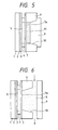
- Fig. 5 is a typical view illustrating another liquid crystal display device of the present invention.
- Fig. 6 is a typical view illustrating another liquid crystal display device of the present invention.
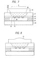
- Fig. 7 is a typical view illustrating another liquid crystal display device of the present invention.
- Fig. 8 is a typical view illustrating another liquid crystal display device of the present invention.
- Fig. 9 is a typical view illustrating another liquid crystal display device of the present invention.
- Fig. 10 is a typical view illustrating another liquid crystal display device of the present invention.
- Fig. 11 is a typical view illustrating an active matrix substrate useful in the liquid crystal display device of the present invention.
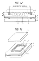
- Fig. 12 is a typical cross-sectional view illustrating the liquid crystal display device of the present invention.
- Fig. 13 is a perspective view showing the state before enclosing a potting material 8, with a sealing substrate for the liquid crystal display device of Fig. 12 removed.
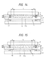
- Fig. 14 is a typical view illustrating another liquid crystal display device of the present invention.
- Fig. 15 is a typical view illustrating another liquid crystal display device of the present invention.
- Fig. 16 is a typical view illustrating another liquid crystal display device of the present invention.
- Fig. 17 is a typical view illustrating another liquid crystal display device of the present invention.
- Figs. 18A and 18B are typical views illustrating another liquid crystal display device of the present invention.
- Fig. 19 is a typical view illustrating another liquid crystal display device of the present invention.
- Figs. 20A and 20B are typical cross-sectional views illustrating the liquid crystal display device of Fig. 19.
- Fig. 21 is a typical plan view illustrating another liquid crystal display device of the present invention.
- Fig. 22 is a typical plan view illustrating another liquid crystal display device of the present invention.
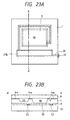
- Figs. 23A and 23B are typical views illustrating another liquid crystal display device of the present invention.
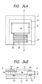
- Figs. 24A and 24B are typical views illustrating another liquid crystal display device of the present invention.
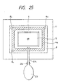
- Fig. 25 is a typical view illustrating another liquid crystal display device of the present invention.
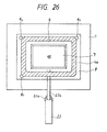
- Fig. 26 is a typical view illustrating another liquid crystal display device of the present invention.
- Fig. 27 is a typical plan view illustrating another liquid crystal display device of the present invention.
- Fig. 28 is a typical plan view illustrating another liquid crystal display device of the present invention.
- Fig. 29 is a typical plan view illustrating another liquid crystal display device of the present invention.
- Fig. 30 is a typical plan view illustrating another liquid crystal display device of the present invention.
- Fig. 31 is a typical plan view illustrating another liquid crystal display device of the present invention.
- Figs. 32A and 32B are typical views illustrating another liquid crystal display device of the present invention.
- Fig. 33 is a typical plan view illustrating another liquid crystal display device of the present invention.
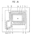
- Fig. 34 is a typical plan view illustrating another liquid crystal display device of the present invention.
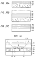
- Figs. 35A to 35C are typical views showing a manufacturing method of the Si substrate applicable to the liquid crystal display device of the present invention.
- Fig. 36 is a typical cross-sectional view illustrating another liquid crystal cell of the present invention.
- Fig. 37 is a typical cross-sectional view illustrating another liquid crystal cell of the present invention.
- Fig. 38 is a typical cross-sectional view illustrating another liquid crystal cell of the present invention.
- Figs. 39A to 39C are typical views showing a manufacturing process of the liquid crystal cell of Fig. 36.
- Figs. 40A to 40C are typical views showing another manufacturing process of the liquid crystal cell of Fig. 36.
- Figs. 41A and 41B are typical views illustrating another liquid crystal display device of the present invention.
- Figs. 42A to 42C are typical views for illustrating a manufacturing method of the device of the present invention.
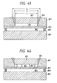
- Fig. 43 is a typical cross-sectional view illustrating another liquid crystal display device of the present invention.
- Fig. 44 is a typical cross-sectional view illustrating another liquid crystal display device of the present invention.
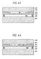
- Fig. 45 is a typical cross-sectional view illustrating another liquid crystal display device of the present invention.
- Fig. 46 is a typical cross-sectional view illustrating another liquid crystal display device of the present invention.
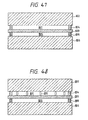
- Fig. 47 is a typical cross-sectional view illustrating another liquid crystal display device of the present invention.
- Fig. 48 is a typical cross-sectional view illustrating another liquid crystal display device of the present invention.
- Figs. 49A and 49B are typical schematic views illustrating another liquid crystal display device of the present invention.
- Figs. 50A to 50C are typical schematic views illustrating another liquid crystal display device of the present invention.
- Figs. 51A and 51B are typical views illustrating another liquid crystal display device of the present invention.
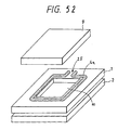
- Fig. 52 is a typical view illustrating a process for making the potting material filling region according to the present invention.
- Figs. 53A and 53B are typical views illustrating another liquid crystal display device of the present invention.
- a liquid crystal display device of the present invention is comprised of picture element electrodes provided on the first plane of a substrate and an opposed electrode placed opposedly to said picture element electrodes, between which a liquid crystal is carried, wherein in a region of said substrate corresponding to said picture element electrodes is formed a concave portion from the second plane side opposite the first plane of said substrate, said region being light translucent, and said concave recess or portion being sealed by a transparent substrate to form a space therein, and a light transparent and liquid filling material being sealed within the space.
- liquid crystal display devices of the present invention are also included the appropriately improved liquid crystal display devices of the above constitution.
- a light transparent material enclosed into the concave recess or cavity prevents the variation in the thickness of liquid crystal gap. That is, because the pressure equivalent to the internal pressure of liquid crystal is exerted on the thin film being translucent from the opposite side, the membrane portion composed of the thin film is prevented from flexing due to dead weight of liquid crystal, so that there is no difference in the cell gap amount of liquid crystal between sites. Also, because of no thermal stress acting on the thin film, driving elements on the thin film undergo no thermal stress, thereby causing only minimum variation in the characteristics, and resulting in less degradation in the display quality of liquid crystal. Hence, the quite high quality display image can be obtained stably.
- liquid crystal display device of the present invention it is possible to adjust the volume change of the translucent material enclosed into the concave portion due to temperature change to be substantially equivalent to that of the concave portion.
- the liquid crystal display device of the present invention may be configured to reinforce the thin film layer provided with liquid crystal driving elements by filling the liquid filling material in the concave portion, and enhance the environment resistance by providing a region for absorbing volume changes of the liquid filling material reinforcing the thin film layer which occur due to varying temperature or atmospheric pressure, outside of the image display portion.
- the liquid crystal display device of the present invention may be configured to enclose, as the liquid filling material a resin in a certain thickness or below on the surface of thin film which is the bottom of the concave portion, and enclosing an inert gas into remaining portion.
- the liquid crystal display devices of the present invention also include a liquid crystal display device in which two substrates have a thin film layer provided with liquid crystal driving elements sandwiched therebetween, one of the substrates having the liquid crystal material and the other having the liquid filling material, wherein the two substrates are transparent, and a transparent electrode is provided on the surface of the transparent substrate enclosing the liquid crystal material, and a light shielding layer and color filters are provided on the surface of the transparent substrate enclosing the liquid filling material.
- the liquid crystal display devices of the present invention also include a liquid crystal display device in which there are provided two substrates having a liquid crystal driving element layer sandwiched therebetween, with a liquid crystal material provided between one substrate and the liquid crystal driving element layer, and the liquid filling material provided between the other substrate and the liquid crystal driving element layer, wherein the two substrates are transparent, and the volume of the liquid crystal material is equal to or greater than that of the liquid filling material.
- the liquid crystal display devices of the present invention also include a liquid crystal display device in which a liquid crystal panel has a liquid crystal carried between a liquid crystal driving element substrate having a liquid crystal driving element layer via a transparent insulating layer on an opaque substrate, and a transparent opposed substrate having a transparent electrode on a transparent substrate, the opaque substrate corresponding to a display area of the liquid crystal panel is hollowed up to the transparent insulating layer, the liquid filling material is disposed in a hollow portion, and enclosed via the elastic sealing member by a transparent sealing substrate.
- the present invention can exhibit the excellent effect in the liquid crystal display device having mounted the driving elements composed of single crystal Si but is not limited to such liquid crystal display devices employing single crystal Si, and the present invention may be applicable to the conventional liquid crystal display devices employing polycrystalline Si, amorphous Si or other semiconductors.
- the volume change of the transparent and liquid filling can be absorbed by the resiliency of sealing member used for the sealing of the transparent material, preventing the influence on the liquid crystal layer or driving elements.
- 1 is a transparent substrate
- 2 is a light shielding layer for shielding light between a color filter layer corresponding to each picture element and the picture element
- 3 is a common electrode for applying a voltage to the liquid crystal
- 4 is a liquid crystal seal area
- 5 is a liquid crystal, the seal area 4 defining the layer thickness of the liquid crystal 5.
- 6 is a silicon SOI substrate where picture element area is hollowed out to be translucent (light transmitting) (i.e., a concave portion is formed)
- 7 is a thin film provided with an electrode for applying a voltage to liquid crystal, a transistor and a driving circuit for each picture element, wherein the portion residing on the upper side of a hollow portion 10 is a membrane portion 7a.
- a translucent liquid 8 having a specific weight equal to that of liquid crystal, as the light transparent material is filled in the hollow portion 10, and enclosed by covering the hollow portion 10 with a transparent substrate 9.
- this translucent liquid 8 By causing this translucent liquid 8 to exert a pressure equal to or greater than the internal pressure of the liquid crystal layer from the opposite side, the forces pressing on the membrane portion 7a from left and right sides are equalized for each section to cause the force of the liquid crystal 5 pressing on the membrane portion 7a to be balanced for each section, so that no flexure of the membrane layer 7 occurs.
- This liquid crystal display device is of a sealed structure which excludes any contaminant such as alkali, giving rise to a higher reliability.
- the transparent substrate 9 is favorably composed of an inorganic material such as glass which allows no water to percolate thereinto to provide a better temperature resistance.
- Fig. 5 is an example wherein a liquid crystal 11 identical to liquid crystal 5 within the liquid crystal cell is filled by the same volume into the hollow portion 10 to balance the pressing forces from left and right sides onto the membrane 7.
- a transparent substrate 9 sealing the liquid crystal 11 is attached to partially enter the hollow portion 10.
- Fig. 6 is an example in which a liquid 8 with the same dead weight filled in the hollow portion 10 is circularly flowed.
- the force of the liquid crystal pressing on the membrane portion 7a is balanced for each section, and the heat generated in the panel portion is absorbed by virtue of the circular flow to maintain the temperature constant. Therefore, it is suitable for usages such as a projection TV which has high brightness and causes significant temperature elevation.
- the translucent liquid 8 having a specific weight equal to that of liquid crystal and the same liquid crystal 11 are provided, it will be appreciated that other materials can be also used.
- Fig. 7 is an example in which a potting resin 36 as the light transparent material is filled in the hollow portion 10.
- the manufacturing method of a display device as shown in Fig. 7 is as follows.
- a thin film is formed on a substrate 21 made of single crystal silicon as the main component which is an SOI substrate or semiconductor substrate.
- the thin film 22 is composed of an insulating layer as well as an active layer of the SOI substrate 21, and a deposited layer formed in the postprocess, whereby driving elements 24 for driving the liquid crystal and electrodes 25 are formed in this thin film 22 to fabricate an active matrix circuit substrate.
- a glass substrate 28 having an opposed electrode 29 is bonded by the sealing member 27, and thereafter a liquid crystal 26 is transferred into the gap between both substrates and sealed by a well-known method.
- a liquid crystal display portion A is necessary to be made transparent, and thus is formed into the hollow portion 10 by removing a single crystal silicon portion of the SOI substrate by anisotropical etching with an alkaline etching liquid, until a portion of the thin film 22 is exposed. Thereafter, a transparent potting resin 36 is filled into the hollow portion 10 to provide reinforcement.
- the potting resin 36 for use may be gel-type silicon resin such as KJR-9010 made by The Shin-Etsu Chemical Co., Ltd., for example.
- Adhesive for use may be a UV curable resin (epoxy type, unsaturated polyester type, acrylate type, thiol type, salt type) which is curable at temperatures practically used, or an instantaneous adhesive of two liquid mixture type.
- a liquid crystal cell filled with resin can be obtained as shown in Fig. 7.
- the optical scattering can be prevented to improve the visibility.
- a resin having a refractive index approximating that of the thin film and a transparent substrate a brighter liquid crystal display device with lowered interfacial scattering and better transmittance can be provided.
- Fig. 11 illustrates an active matrix circuit substrate usable in this example.
- a CMOS converter is used for the peripheral driving circuit, and a PMOS transistor is used for the switching element of picture element electrode.
- 61 is a supporting substrate
- 62 is a backing insulating layer
- 63 is an element separating oxide film
- 64 is a source region of NMOS transistor
- 65 is a drain region of NMOS transistor
- 66 is a drain region of PMOS transistor
- 67 is a source region of PMOS transistor
- 68 is a gate oxide film
- 69 is a gate electrode
- 70 is a channel region of NMOS transistor
- 71 is a channel region of PMOS transistor
- 72 is an N-type electric field relaxation region
- 73 is a P-type electric field relaxation region
- 74 is an A1 (wiring) electrode
- 75 is an NMOS transistor
- 76, 77 is a PMOS transistor
- 78 is a holding capacitor
- 79 is a CMOS inverter
- 80 81 is an interlayer insul
- an optical element e.g., a lens 31 may be incorporated in a package member, as shown in Fig. 8.
- an illumination system used in the liquid crystal cell or optical system on the visual field side can be simplified, allowing the system to be smaller with its costs reduced.
- a liquid crystal may be filled in the same manner as shown in Fig. 7, whereupon the flexure of membrane portion 7a can be similarly eliminated and the variation in thickness of the liquid crystal gap is prevented.
- the light transparent material 32 composed of such liquid crystal may be sealed by a glass plate with a convex lens 33.
- the sealing member is not limited to glass, but may be sufficient with a member which can transmit the light such as a plastic plate.
- the reliability of the liquid crystal display device having one electrode formed on the thin film is significantly improved. Also, for this reason, the display quality will not degrade and the decrease in manufacturing yield can be prevented, whereby it is possible to lower the price of products. Since other optical system can be also incorporated, the total system can be made smaller with its costs reduced.
- Fig. 12 is a cross-sectional view showing a liquid crystal display device of this example.
- a circuit substrate 1 is non-translucent, and has Tufts and other driving circuit formed via an insulating layer on the surface thereof.
- an opposed substrate 2 which is translucent such as glass is attached by a seal member 4, and a liquid crystal 5 is enclosed between them.
- transmissent means to allow visible light to pass through.
- a hollow portion 10 is formed to thereby afford a translucent nature to the region of the circuit substrate 1 corresponding to the display area.
- a sealing substrate 9 which is translucent such as glass is attached via the seal member 4a, and a potting material 8 is enclosed between the circuit substrate 1 and the sealing substrate 9.
- This potting material 8 has a less stiffening, flowable nature in the temperature range in which the liquid crystal display device is practically used, and serves as the translucent material.
- the seal member 4a may be silicon resin or epoxy resin, for example, and the potting material 8 may be polyethylene glycol, a transparent liquid crystal material or silicon-type gel.
- Fig. 13 is a perspective view showing the state before enclosing the potting material 8, with the sealing substrate 9 removed.
- the seal member 4a for bonding the sealing substrate 9 with the circuit substrate 1 is laid to surround the outside of the hollow portion 10. Also, on one side of the area surrounded by the seal members 4a is formed an inlet port 4b for transferring the potting material 8.
- the potting material 8 is transferred through the inlet port 4b between the circuit substrate 1 and the sealing substrate 9 after bonding the sealing substrate 9 via the seal member 4a to the circuit substrate 1, and hermetically enclosed by sealing the inlet port 46 with a sealing material as will be described later.
- a membrane portion 10a left behind by formation of the hollow portion 10 is covered with the potting material 8 and the sealing substrate 9, and protected from the variation in humidity or atmospheric pressure.
- the practical use of the liquid crystal display device is normally effected in the temperature range from about -20 to +60°C. Accordingly, it is necessary not to apply any excessive pressure to the membrane portion 10a left behind by formation of the hollow portion 10 in this temperature range.
- the volume change of potting material due to temperature variation is set to be substantially equal to the volume change between the circuit substrate 1 and the sealing substrate 9, which is caused by the volume change of the seal member 4a varying the spacing between the circuit substrate 1 and the sealing substrate 9.
- d 1 and d 2 are defined as shown in Fig. 12, and assuming that the length of one side for the display region corresponding to the width of hollow portion 10 is L, the interval from the side edge of hollow portion 10 to the seal member 4a is 1, the coefficient of linear expansion for the seal member 4a in the longitudinal direction is ⁇ (K -1 ), the coefficient of cubic expansion for the potting material 8 is ⁇ (K -1 ), and the temperature variation is T(K), wherein 1 «L is supposed, d 1 ⁇ L 2 T ⁇ (d 1 +d 2 ) ⁇ L 2 T
- the left side indicates the volume change regarding the potting material 8 enclosing region due to expansion (shrinkage) of the seal member 4a, while the right side indicates the volume change of potting material 8.
- d 2 is equal to 600 ⁇ m and d 1 is equal to 5mm.
- the coefficient of cubic expansion ⁇ for ethylene glycol is 0.64x10 -3 (K -1 ).
- a variety of silicon resins are made wherein the coefficient of linear expansion in its longitudinal direction can be selected in a range from 0.1 to 10x10 -3 (K -1 ).
- ⁇ 0.7x10 -3 (K -1 ) is selected, so that the above expression (B) can be satisfied.
- each of ⁇ and ⁇ slightly varies with the temperature, but as the design value, the average value in the temperature range for practical use may be adopted.
- the opposed substrate 2 and the circuit substrate 1 are bonded via the seal member 4, and after a liquid crystal 5 is transferred between them and then sealed, the hollow portion 10 is formed in the circuit substrate 1 to leave behind the membrane portion 10a.
- the transfer and sealing of the potting material 8 is performed, and this is divided into three processes including laying the seal member 4a, transferring the potting material 8 and sealing the inlet port 4b (see Fig. 13).
- the seal member 4a is applied around the hollow portion 10. This application can be effected by tracing a shape discharged through the tip end of needle from the dispenser, or by squeegee printing. In making this application, the inlet port 4b is formed as shown in Fig. 13.
- the sealing substrate 9 such as glass is placed on the seal member 4a applied, a pressure is exerted so that the circuit substrate 1 and the sealing substrate 9 may be overlapped with a desired gap, and by burning (e.g., in an oven for two hours at 80°C), the filling region of the potting material 8 is formed.
- the gap between the circuit substrate 1 and the sealing substrate 9 can be controlled by disposing a gap member having a desired thickness, for example, a glass or a needle, between the circuit substrate 1 and the sealing substrate 2. Also, when a very narrow gap (e.g., about 10 ⁇ m) is required, beads having a diameter roughly corresponding to this gap may be mixed into the seal member 4a, when applied, to thereby provide the desired gap.
- a gap member having a desired thickness for example, a glass or a needle
- the filling of potting material 8 can be effected by a conventionally well-known vacuum transfer method.
- the potting material 8 is subjected to vacuum degassing (e.g., for twelve hours at 0.133 Pa (10 -3 Torr)) before transfer to exclude any mixture of bubbles.
- the liquid crystal display device (liquid crystal cell) having formed the filling area of the potting material 8 between the circuit substrate 1 and the sealing substrate 2 and the potting material 8 placed in a Petri dish are set within a vacuum apparatus to draw a vacuum to a degree of vacuum of about 0.133 Pa (10 -3 Torr).
- the time of drawing vacuum is about one to twenty-four hours after having reached 0.133 Pa (10 -3 Torr).
- the liquid crystal display device is immersed in the Petri dish containing the potting material 8 still in vacuum state.
- the potting material 8 enters the filling region to some extent due to capillary phenomenon.
- the vacuum apparatus After the transfer with the capillary phenomenon arrives at an equilibrium state, the vacuum apparatus is gradually leaked for a period from twenty minutes to one hour to allow the potting material 8 to be sufficiently transferred into the filling region.
- the potting material 8 is preferably a material having low vapor pressure.
- the liquid crystal display device is taken out from the vacuum apparatus, and after the inlet port 4b is cleanly wiped with acetone and degreased, the sealing of the inlet port 4b is effected by mounting a sealing material.
- the sealing material may be epoxy resin when the potting material 8 used is polyethylene glycol.
- Fig. 14 is a variation of Fig. 12. This variation of Fig. 14 is similar to Fig. 12, except that a groove 11 is formed in the site of laying the seal member 4a to the circuit substrate 1, and the seal member 4a is laid within this groove, whereby the substantially thicker application of the seal member 4a can be made without increasing the interval between the circuit substrate 1 and the sealing substrate 9.
- the volume change of the seal member 5 can be larger than that of Fig. 12, whereby this variation can follow the instance where the volume change of the potting material 8 is large.
- groove 13 is formed simultaneously with the formation of hollow portion 10 (normally by etching), the increase in the number of processes can be avoided.
- depth of groove 13 is equal to that of hollow portion 10 in this example, it should be noted that this depth of groove 13 may be selected in accordance with the quality of potting material 8 for use and the quality of seal member 4a.
- the condition that the volume change of the potting material 8 with temperature change may be substantially equal to the volume change between the circuit substrate 1 and the sealing substrate 9 caused by the volume change of the seal member 4a with temperature change is, when 1 «L, (d 1 +d 2 ) ⁇ L 2 T ⁇ (d 1 +d 2 ) ⁇ L 2 T namely ⁇ ⁇ ⁇
- Fig. 15 is a typical view showing a further variation. This variation as shown can exhibit the same effects as that of Fig. 14 by making the hollow portion 10 a wider area including the range for laying the seal member 4a.
- Fig. 16 is a typical view showing another variation. This variation as shown in equivalent to that of Fig. 15, except that the sealing substrate 9 is of a convex shape in cross section in which its central portion protrudes toward the hollow portion 10 so that the display region is thick and the peripheral seal region is thin.
- the sealing substrate 6 is thick in the display region, the volume of potting material 8 can be reduced, and the selection width of the seal member 4a can be widened.
- the condition that the volume change of the potting material 8 with temperature change may be substantially equal to the volume change between the circuit substrate 1 and the sealing substrate 9 caused by the volume change of the seal member 4a with temperature change is (d 1 +d 2 ) ⁇ ⁇ (d 1 -d 2 ) ⁇ when 1 «L, and using d 1 and d 2 as shown in Fig. 16, whereby ⁇ can be set smaller than that of the examples of Figs. 12 to 15 for the same ⁇ .
- Fig. 17 is a typical view of another variation.
- This variation uses a sealing substrate 9 of convex shape in cross section, like the example of Fig. 16, instead of the sealing substrate 9 in the example of Fig. 12.
- the coefficient of cubic expansion for the potting material 8 is necessary to be smaller than in the example of Fig. 16, wherein there is the advantage that the mounting state of the seal member 4a is stabler than in the example of Fig. 16.
- Fig. 18A is a plan view of a liquid crystal display device in this example, and Fig. 18B is a cross-sectional view taken along the line A-A'.
- the liquid crystal display device of this example consists of an image display liquid crystal cell portion and a potting cell portion for reinforcing the liquid crystal cell portion by transferring the potting material.
- the liquid crystal cell portion is comprised of a liquid crystal 50 transferred into a portion surrounded by a transparent substrate 51, a liquid crystal driving element layer 60, and a frame member as the seal member 52.
- the transparent substrate 51 is provided with a light shielding layer for shielding light between color filters, a transparent electrode for applying a voltage to liquid crystal, and an oriented film for orienting the liquid crystal in a fixed direction.
- the liquid crystal driving element layer 60 is comprised of a picture element electrode, a thin film transistor (TFT) for applying a signal to the electrode, a signal line for sending the signal to TFT, a TFT driving line, for each picture element section, and horizontal and vertical shift registers for driving the picture element Tufts.
- TFT thin film transistor
- the liquid crystal driving element layer 60 is made on an Si substrate manufactured by the method as shown in Figs. 35A to 35C.
- the Si substrate is an Si single crystal substrate which is superior in economical aspect and has extremely excellent crystallinity to be uniformly flat over the large area.
- the semiconductor active elements are made on the Si single crystal layer having significantly less defects, so that the floating capacity of semiconductors is reduced, whereby it is possible to provide high performance liquid crystal display devices wherein the elements and circuits capable of effecting high speed operation, no latch-up phenomenon, and excellent radiation resistance characteristic are integrated on the same substrate as that of the liquid crystal image display picture elements.
- a manufacturing method of the Si substrate will be exemplified below with reference to Figs. 35A to 35C.
- a porous Si substrate is formed by anodizing a P-type (100) monocrystalline Si substrate having a thickness of 300 ⁇ m (microns) in an HF solution.
- Si epitaxial layer 102 with a thickness of 1.0 micron is grown on the P-type (100) porous Si substrate 101 thus obtained by low-pressure CVD.
- Deposition is conducted under the following conditions: Source gas SiH 4 Carrier gas H 2 Temperature 850°C Pressure 1.33 Pa (1x10 -2 Torr) Growth rate 3.3nm/sec
- a 100nm (1000 ⁇ ) thick oxide layer 103 is formed on the surface of the epitaxial layer 102, and on its oxide surface is placed another Si substrate 107 formed with a 500nm (5000 ⁇ ) thick oxide layer 104 and a 100nm (1000 ⁇ ) thick nitride layer 105, as shown in Fig. 35B.
- the whole structure is then heated at 800°C in an nitrogen atmosphere for 0.5 hours to firmly join the two substrates to each other.
- the etching rate of the non-porous Si single-crystal with the etching solution is extremely low, such that the etching layer is 5nm (50 angstroms) thick or less even 65 minutes later, and the selective ratio of the etching rate of the porous layer to that of the non-porous Si single-crystal is as large as 10 5 or more, as shown in Fig. 35C.
- the etched amount in the non-porous layer is a practically negligible decrease.
- the Si substrate 101 having a thickness of 200 ⁇ m (microns), rendered porous, is removed, and a single-crystal Si layer 102 having a thickness of 1.0 ⁇ m is formed on the SiO 2 103.
- SiH 2 Cl is used as the source gas, the growth temperature has to be higher by several tens of degrees. However, high-speed etching characteristic peculiar to the porous substrate is maintained.
- TFT is formed on the single crystal silicon thin film 102 to provide a liquid crystal driving element layer 60, which is opaque to visible light because the liquid crystal driving element layer 60 is made on the Si substrate 1.
- a liquid crystal driving element layer 60 which is opaque to visible light because the liquid crystal driving element layer 60 is made on the Si substrate 1.
- the etching solution used is tetramethyl ammonium hydride (TMAH) aqueous solution.
- TMAH tetramethyl ammonium hydride
- the etching conditions are 22% TMAH aqueous solution, 90°C and ten hours.
- the Si substrate 1 of a structure where a thin insulating layer resides on the Si substrate and a single crystal Si layer is laid on its upper portion (Silicon On Insulator structure, SOI), because the insulating layer 7 serves as the etching stop layer to be effective for the uniform etching.
- the etching solution is not particularly limitative as far as the selection ratio of Si to SiO 2 can be sufficiently attained such as KOH.
- This method is largely divided into three processes including making the potting material filling region, transferring the potting material and sealing the inlet port. In the following, these processes will be described in this order.
- the Si substrate 1 is hollowed by etching to provide a region 20 for absorbing potting material volume change, a passageway for connecting the opening portion 10 to the region 20 for absorbing potting material volume change, and a passageway for connecting the opening portion 10 to the potting material inlet port 25 at the same time while the opening portion 10 is being etched.
- an adhesive (seal or frame member 4a) is applied onto the Si substrate 1 around the region 20 for absorbing potting material volume change.
- the frame member used was epoxy resin (Structbond EH454NF made by Mitsui Toatsu Chemicals, Inc.).
- the frame member 4a with adhesive may be formed either by discharging adhesive through the tip of needle to trace a pattern, or by squeegee printing.
- the glass substrate 9 made of a material having a thermal expansion coefficient approximating that of the Si substrate 1, because it is effective to suppress the warpage of liquid crystal display device.
- the glass substrate 9 used was AL glass made by Asahi Glass Co., Ltd., having a thermal expansion coefficient relatively approximating that of Si (thermal expansion coefficient of 36x10 -7 for AL glass, and 32x10 -7 for Si).
- the gap was suppressed by carrying a gap member (glass or needle) having a desired thickness between the glass substrate 9 and the Si substrate 1.
- the frame member 4a is formed into a desired gap thickness by mixing beads (Micropeal SP made by Sekisui Fine Chemical) having a diameter of about 10 ⁇ m in the epoxy resin.
- the potting material is subjected to vacuum degassing (e.g., for twelve hours at 0.133 Pa (10 -3 Torr)) before transferring to exclude any mixture of bubbles.
- the liquid crystal display device liquid crystal cell
- the time of drawing vacuum is from about one to twenty-four hours after having reached 0.133Pa (10 -3 Torr).
- the liquid crystal cell is immersed in the potting material by placing it in the Petri dish containing the potting material still in vacuum state. After the transfer with the capillary phenomenon reaches an equilibrium state, the vacuum apparatus is gradually leaked for a period from twenty minutes to one hour to sufficiently transfer the potting material into the frame.
- the potting material is transferred in a vacuum of about 0.133 Pa (10 -3 Torr) as above described. Therefore, the potting material is necessary to be a liquid which has a low vapor pressure, is transparent and is neither solidified nor gasified in a temperature range from -20°C to 80°C.
- the potting cell used contained liquid crystal, polyethylene glycol (Polyethylene glycol #200 made by Kanto Chemical), silicone oil (Shinetsu Silicone made by The Shin-Etsu Chemical Co., Ltd.).
- the sealing of the opening is performed in the following way.
- the liquid crystal cell is taken out from the vacuum apparatus, and the inlet port 25 is cleanly wiped with acetone and degreased.
- the sealing of the inlet port 25 for potting material is effected by mounting sealing material 22.
- the sealing material used was epoxy resin (Structbond ES280 made by Mitsui Toatsu Chemical) or ultraviolet curable resin when the potting material was liquid crystal and polyethylene glycol, while it was Silicone Bond (Shinetsu Silicone made by The Shin-Etsu Chemical Co., Ltd.) when the potting material was silicone oil.
- the curing was made at room temperature for twelve hours when epoxy resin was used. In the case of silicon resin, the curing was made at 80°C for two hours.
- the sealing time for ultraviolet curable resin is as short as one minute for applying ultraviolet radiation, so that the sealing is very effectively made firmly and rapidly.
- the liquid crystal display device of this example makes the display in the opening portion 10 by driving the liquid crystal 50 of the opening portion 10 by means of the liquid crystal driving elements fabricated in the liquid crystal driving element layer 60. Since the distance between the glass substrate 51 and the liquid crystal driving element layer 60 defined by the frame member 52 (hereinafter referred to as the gap) affects the transmittance of light, it is desirable that the cell gap is uniform over the entire face of the opening portion 10 to effect even display over the entire face. In this example, the thickness of liquid crystal driving element layer 60 is as thin as one-thousandth or less the opening area, so that the liquid crystal driving element is liable to deformation and cracks. Therefore, the structure as reinforced by potting as shown in this example can enhance the durability and reliability in this liquid crystal display device, and is very effective to provide higher image quality.
- the liquid crystal display device of this example has a structure of absorbing the volume change of potting material with the temperature or atmospheric pressure variation by virtue of the deformation of rubber film 21, and is strong to variations in environment.
- Fig. 19 is a plan view of a liquid crystal display device of this example.
- Fig. 20A is a cross-sectional view taken along the line A-A'
- Fig. 20B is a cross-sectional view taken along the line B-B'.
- the liquid crystal display device of this example is a variant of the liquid crystal display device of the example 3.
- This example has a feature that the depth of hollow by etching the region 23 for absorbing potting material volume change and the depth of hollow by etching the passageway connecting the opening portion 10 to the region 20a for absorbing potting material volume change and the passageway connecting the opening portion 10 to the potting material inlet port 25 are shallower than that of the opening portion 10.
- the region of shallower hollow other than the opening portion 10 is masked with a material having a masking effect against TMAH such as a Teflon tape or silicon resin. After the opening portion 10 is etched to a desired depth, the mask is removed, and the opening portion 10 is further etched until it reaches an insulating layer 7. In this manner, the above structure can be realized.
- TMAH a masking effect against Teflon tape or silicon resin.
- Fig. 21 The feature of this example resides in that there are formed a plurality of regions 20 for absorbing potting material volume change.
- the depth of hollow for the region 20 for absorbing potting material volume change is equal to the depth of hollow for the opening portion 10.
- a structure can be realized in which at least one of the plurality of regions 20 for absorbing potting material volume change is shallower than the depth of hollow for the opening portion 10.
- Fig. 22 The feature of this example resides in that there are formed a plurality of regions 20a for absorbing potting material volume change which have a shallower hollow than the opening portion 10. There is also a possible structure in which the regions 20a for absorbing potting material volume change are all equal depth of hollow, or except for at least some hollows.
- Fig. 23A is a plan view of a liquid crystal display device of this example
- Fig. 23B is a cross-sectional view taken along the line A-A'.
- the feature of this example resides in that there is provided a region 20b for absorbing potting material volume change which has a gas enclosed.
- the enclosed gas may occupy a part or a whole of the region 20b for absorbing potting material volume change.
- a forming method of the potting cell and an enclosing method of gas will be described below.
- a potting cell is formed in such a way that after hollowing into a desired pattern by etching, a seal or frame member 4a is applied around the hollow portion, and a glass plate 9 is placed thereon.
- the potting material is transferred by the vacuum transfer method, the whole structure is heated up to about 100°C in a desired gas atmosphere, and held for about one hour. Thereafter, it is gradually cooled down to room temperature, and the potting material inlet port 25 is sealed with a sealing material.
- another sealing method is possible in which after the potting material is transferred, a vacuum is drawn again, a desired amount of potting material is extracted from within the cell, and a desired gas is leaked to restore the cell to an ordinary pressure, whereby the sealing is effected.
- Fig. 24A is a plan view of a liquid crystal display device of this example
- Fig. 24B is a cross-sectional view taken along the line A-A'.
- the feature of this example resides in that the potting material inlet port 25 is sealed, the distance of a passageway 27 from the potting material inlet port 25 to the opening portion 10 is lengthened, with its cross section made smaller.
- the length l of a passageway 27 and its cross section S are defined as follows. First, the cross section S is 1mm 2 or less.
- Fig. 25 is a typical view of a liquid crystal display device of this example.
- the feature of this example resides in that there is provided a rubber bag 23 for absorbing the potting material volume change at one tip of a needle 23a.
- a forming method of the potting cell of this example will be described below.
- a potting cell is formed in such a way that after the opening portion 10 is hollowed out by etching, a frame (seal) member 4a is formed, the needle 23a is installed to serve as a passageway between the inside and the outside of the frame member 4a, and a glass plate 9 is placed thereon.
- a plurality of spacers 4c are disposed.
- the potting material is transferred to the end of the needle 23a outside the cell, and the rubber bag 23 entirely filled with the potting material is mounted to the end of the needle 23a.
- the mounting portion is sealed with an epoxy type resin 22a curable at room temperature, and held at room temperature for the curing for twelve hours or more.
- the image display portion can be reinforced with potting material, resulting in the greater strength against the environmental changes. Also, it is possible to make a plurality of regions for absorbing potting material volume change comprised of the needle 23a, the rubber bag 23 and the sealing member 22a.
- Fig. 26 is a typical view of a liquid crystal display device of this example.
- the feature of this example resides in that there is provided a flexible tube 23 made of vinylchloride. A forming method of the potting cell of this example will be described below.
- a cell portion comprised of a frame member 4a, a glass plate 9 and a spacer 4c is formed, and the tube 23 is attached to the end of needle 23a outside the cell, and sealed with a sealing member 22a. Thereafter, the potting material is transferred in vacuum from another opening of the tube 23, the tube is then compressed to reduce the internal volume, and the inlet port is hermetically sealed by the use of a soldering iron.
- the internal volume V of tube and the volume V of deformed tube are defined as follows.
- V-V 1 > V P (Room) - V P (-20°C)
- V 1 > V P (80°C) - V P (Room)
- V P (Room) is the total volume of potting material within the potting cell at room temperature
- V P (-20°C) is the volume of the same potting material at -20°C
- V P (80°C) is the volume of the same potting material at 80°C.
- Fig. 27 is a typical view of a liquid crystal display device of this example.
- the feature of this example resides in that a gas is partially enclosed into a vessel 23.
- the volume V GAS of filler gas is defined as follows. V GAS > V P ( 80°C) - V P (Room) Where V P (Room) is the total volume of potting material within the potting cell at room temperature, and V P (80°C) is the volume of the same potting material at 80°C.
- the diameter of needle 23a is 0.5mm or less.
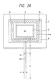
- Fig. 28 is a typical view of a liquid crystal display device of this example.
- the feature of this example resides in that a needle 23b having an open end is provided.
- the diameter d of the needle 23b and the length l of the needle 23b are defined as follows.
- d is 0.5mm or less.
- d ⁇ l 1 > V P (Room) - V P (-20°C) d ⁇ l 2 > V P (80°C) - V P (Room) 1 l 1 +l 2
- V P (Room) is the total volume of potting material within the cell at room temperature
- V P (80°C) is the volume of the same potting material at 80°C
- V P (-20°C) is the volume of the same potting material at -20°C.
- the potting material liquid plane 16 is set by filling the potting material up to the end of the needle 23b outside the cell, holding the cell at 80°C or higher for one hour, and then gradually cooling the cell. Or there is likewise a method in which the potting material is filled to the end of the needle 23b, and a desired potting material is extracted out of the cell by drawing a vacuum.
- a plurality of needles 23b can be set, and when the number is n, the length of respective needle 23b is 1/n that of 1.
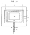
- Fig. 29 is a typical view of a liquid crystal display device of this example.
- the feature of this example resides in that a film 13 such as Goatex which can transmit the gas but not the liquid is provided.
- the length of the needle 23b is the same as defined in the example 12.
- the film 13 is attached after transferring the potting material and setting a desired potting material liquid plane 16, and sealed with a sealing material.
- Fig. 30 is a typical view of a liquid crystal display device of this example.
- the feature of this example resides in that a padding 34 such as a sponge is provided in the needle 23b.
- the length of the needle 23b is the same as defined in the example 12.
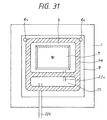
- Fig. 31 is a typical view of a liquid crystal display device of this example.
- the feature of this example resides in that a bubble reservoir region 17 isolated from the opening portion 10 via the frame member 4 and connected through a needle 23c is formed.
- the diameter of the needle 23c is smaller than that of the needle 23b.
- bubbles are prevented from entering the opening portion 10 even if bubbles are passed through the needle 23b.
- Fig. 32A is a plan view of this example and Fig. 32B is a cross-sectional view taken along the line A-A'.
- the feature of this example resides in that a passageway 18 for the potting material is formed by means of a frame member 4a.
- a potting cell is made by forming the frame member 4a into a desired pattern and placing a glass plate 9 thereon. Spacers 4c are provided to make uniform the gap between the glass plate 9 and an Si substrate 1. The diameter of spacers 4c is 0.5mm or less. The length 15 of the passageway 18 from opening portion 10 to potting material inlet port 25 is defined as follows.
- the passageway 18 may consists of a plurality of passageways which are independent of one another. When n passageways in total are formed, the length of each passageway is 1/n that of l 5 .
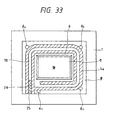
- Fig. 33 is a typical view of a liquid crystal display device of this example.
- the feature of this example resides in that a padding 34 such as a sponge is provided in the passageway 18 inside the potting material inlet port 25.
- the length and height of the passageway 18 are the same as defined in the example 14.
- Fig. 34 is a typical view of a liquid crystal display device of this example.
- the feature of this example resides in that the region for absorbing potting material volume change is formed to enclose the gas therein.
- a gas is introduced into a gas enclosing region 19 in such a manner that after the potting material is transferred through the potting material inlet port 25, the cell is held in a gas atmosphere at a temperature of 90°C or greater for one hour, and gradually cooled, or that the cell is evacuated to extract a desired volume of potting material and a desired gas is leaked to restore the cell to an ordinary pressure. Then, the inlet port 25 is sealed with a sealing material 22 to form a potting cell.
- a liquid crystal display device having a liquid crystal material in one of the intervals between two substrates and a thin film layer provided with liquid crystal driving elements carried therebetween, wherein
- Fig. 36 is a cross-sectional view of a liquid crystal cell of this example.
- This liquid crystal display device has a hollow-type package structure that a thin film 22 is formed using a semiconductor substrate 1 and one electrode 25 is disposed on the surface of thin film, wherein a resin 14 having a thickness equal to or less than a certain value is laminated on the surface of the thin film 22, and an inert gas 15 is filled in remaining thickness portion.
- Fig. 39A 1 is a substrate having single crystal silicon as the main component which is an SOI substrate or semiconductor substrate, wherein a thin film 22 is formed on the substrate 1.
- the thin film 22 is comprised of an insulating layer and an active layer of the SOI substrate 1, and a deposited layer formed by the postprocess, within which thin film 22 are formed driving elements 24 and electrodes 25 for driving the liquid crystal.
- a glass substrate 28 having an opposed electrode 29 is bonded by a seal member 27 (Fig. 39B), and thereafter sealed by transferring a liquid crystal 26 into the gap between both substrates by a well-known method (Fig. 39C).
- a liquid crystal display portion A is necessary to be transparent, and therefore a single crystal silicon portion of the SOI substrate is removed by anisotropical etching with an alkaline etching solution until the thin film portion 22 is exposed to provide a bored (concave) portion 10 (Fig. 40A). Thereafter, transparent potting resin 14 is provided in the bored portion 10 in a desired thickness for the reinforcement (Fig. 40B).
- the potting resin 14 may be a gel-type silicon resin such as KJR-9010 made by The Shin-Etsu Chemical Co., Ltd., for example.
- KJR-9010 made by The Shin-Etsu Chemical Co., Ltd.
- As the curing agent multiple micropellets are dropped in the bored portion 10 to have a thickness of about 60 ⁇ m after mixing and vacuum degassing. This is because it is necessary to evenly spread a resin liquid of relatively high viscosity over the large area in this example.
- the adhesive for use may be a UV curable resin usable at the practical use temperatures (epoxy type, unsaturated polyester type, acrylate type, thiol type, salt type) or an instantaneous adhesive of two liquid mixture type.
- B is an adhesive portion.
- the film thickness of the potting resin is as thin as about 60 ⁇ m, so that the thermal stress exerted on the thin film 22 can be minimum. Accordingly, no flexure of the thin film 22 occurs, with no locational difference in the gap amount of liquid crystal 26. Also, since the thermal stress exerted on the thin film is small, the driving elements 24 on the thin film undergo only a small thermal stress, so that the variation in characteristic is minimum, and there is no change in the display quality of the liquid crystal.
- the potting resin 14 and the inert gas 15 are of the semiconductor grade, no variation in characteristic for the driving elements 24 occurs due to the mixture of mobile ions. Likewise, there is no risk that water contents may be mixed because of the use of the hollow package of sealed type.
- the optical characteristic is substantially ideal because the resin face is smooth and the glass plate is used for the reason as previously described.
- the viscosity of liquid must be lowered, for which it is effective to raise the liquid temperature and reduce the mixture ratio of curing agent.
- the silicon resin has excellent wettability with respect to silicon and thermal oxide film, but when the bad member is used peripherally, it is necessary to enhance the wettability by washing, vapor treatment or plasma treatment.
- the resin thin film which is further flat can be obtained.
- rare gases such as helium, neon, and argon can be used, because these gases are most stable and used in smaller amount, with only slight increase of the costs for the liquid crystal cell.
- the bonding with the glass plate can be made at the highest temperature where the quality of the liquid crystal cell is not degraded, because there is typically a tendency that adhesives usable at low temperature are inferior in the adhesive strength, sealability and reliability.
- Adhesives usable at high temperature may include a thermosetting epoxy resin. It is effective, from the aspect of not giving rise to any excess pressure, that in effecting bonding, the inert gas in the atmosphere is set at a slightly higher pressure, and when cooled down to the practical use temperature, the filled gas is caused to indicate just one atmospheric pressure.
- the adhesion with the glass plate can be made by anodic bonding which requires no adhesive.
- the anodic bonding is required to be made at high temperature and high pressure due to insufficient investigation concerning its principle in the state of the art, but is a technique promising in the future because the complete intimate adhesion is assured without essentially requiring any excess member.
- a pore for adjusting the pressure of gas in the hollow package can be provided in the glass plate.
- the internal pressure of gas may fluctuate due to temperature variation outside, and although the effect of pressing on the thin film is eliminated, the clean gas once filled may escape to the outside, causing some degrade in the image quality.
- a space 49 for adjusting the volume can be further provided outward of the pore 48 provided on the glass plate 46, as shown in Fig. 37.
- the space 49 can be readily constructed by attaching a rubber thin film 50 which is easily deformable with the pressure over the pore.
- the liquid level may rise more or less depending on the value of contact angle at which the material such as silicon forming the peripheral wall face makes contact with the resin.
- the provision of somewhat smaller liquid crystal display plane accounting for the fluctuation of the liquid level may be necessary from the viewpoint of obtaining the uniform display plane.
- This example is not specifically limited to liquid crystal display devices formed by using SOI substrate having single crystal silicon as the main component, but can be readily applied to polysilicon TFTs on the oxide film formed on the single crystal silicon substrate, for example.
- the portion corresponding to the thin film is an upper structure of the oxide film, the polysilicon film and other TFTs.
- this example can be readily applied to semiconductor substrates other than silicon.
- the etching method of removing the silicon for the transparency can be also carried out by isotropic etching.
- the driving element formed on the thin film is not TFT for use in the active matrix but may be only an electrode of simple matrix.
- the method for forming resin on the thin film is only necessary to be capable of forming a thin resin layer, and may be any of atmospheric deposition, vacuum deposition, CVD, plasma deposition, and spin-on method.
- the thickness of resin formed is desirable to vary adequately with the Young's modulus.
- the thin film is spread with a tension of approximately 1 x 10 7 Pa (1x10 8 dyne/cm 2 ), so that the permissible stress for the resin is substantially the same amount. Since the internal stress exerted on typical resin package type ICs is said to be equal to roughly 100MPa (1x10 9 dyne/cm 2 ), the value can be fully accomplished by reducing the thickness of resin film.
- the member in the hollow-type package for use with the present invention is not specifically limited to the glass plate, but may be sufficient with any member which is transparent to the light, such as a plastic plate.
- an optical element such as a lens 51 may be incorporated into the hollow-type package, as shown in Fig. 38.
- the illumination system for use in the liquid crystal cell or the optical system on the visual field side can be simplified, resulting in smaller apparatus and lower costs.
- two or more layers of potting resin 14 can be provided.
- Fig. 41A is a plan view and Fig. 41B is a cross-sectional view of Fig. 41A taken along the line X 1 -X' 1 .
- 41 is a thin film layer outer periphery where a picture element portion and a peripheral circuit are provided
- 42 is a horizontal shift register
- 43 is a picture element peripheral portion
- 44 is a picture element portion where picture element driving transistors are provided.
- 45 is a vertical shift register and 46 is a liquid crystal inlet port and a sealing port.
- a picture element electrode 47 is a picture element electrode, which is connected from the drain of a thin film transistor 49 via a wiring 48 in a contact hole.
- the picture element electrode is disposed on the back side of TFT provided, and a light shielding layer 50 is provided on the TFT through the same process.
- a layer having a large step is provided on the upper layer portion, and a liquid crystal driving portion is provided in the lower layer, whereby the liquid crystal driving can be implemented in the flatter area.
- the light shielding layer is provided above the TFT through the same process, whereby owing to its high alignment precision, the opening ratio is raised, and the bright display can be implemented.
- a liquid crystal display device of this example consists of an image display liquid crystal cell portion and a potting cell portion for reinforcement of the liquid crystal cell with the potting material (flowable material) transferred.
- a fabrication method of this liquid crystal display device will be described below with reference to Figs. 42A to 42C.
- the liquid crystal cell portion is a portion surrounded by a transparent substrate 206, a liquid crystal driving element layer 203 and a frame member 208.
- the transparent substrate 206 is provided with a light shielding layer for shielding the light between color filters and a transparent electrode for applying a voltage to the liquid crystal.
- the liquid crystal driving element layer 203 is comprised of a picture element electrode, a thin film transistor (TFT) for applying a signal to the electrode, a signal line for sending the signal to the TFT, a TFT driving line, for each picture element portion, and horizontal and vertical shift registers for driving the picture element TFTs.
- the liquid crystal layer 205 is enclosed in an interstice between the frame member 208, the transparent substrate 206 and the liquid crystal driving element layer 203.
- the liquid crystal driving element layer 103 is opaque to the visible light because it is made on the Si substrate 207.
- the opening portion 10 is hollowed out by etching so that it is made transparent to the visible light.
- the etching solution used is an aqueous solution of tetramethyl ammonium hydride (TMAH).
- TMAH tetramethyl ammonium hydride
- the etching conditions are 22% TMAH aqueous solution, 90°C and ten hours.
- TMAH tetramethyl ammonium hydride
- SOI Silicon On Insulator structure
- the etching solution may be any solution only if a sufficient selection ratio of Si to SiO 2 can be attained such as KOH.
- an adhesive (frame member 204) is applied on the silicon substrate 207 around the opening portion 10 formed by etching the display region of the Si substrate 207.
- the frame member 204 used is epoxy resin (Structbond EH454NF made by Mitsui Toatsu Chemicals, Inc.).
- the frame member with adhesive may be formed either by discharging adhesive through the point of needle to trace a pattern, or by squeegee printing.
- a glass substrate 202 cut into a desired size is laid thereon, and the whole structure is pressurized to have a desired gap, and burned in an oven at 80°C for two hours to form a potting material filling region.
- the glass substrate 202 made of a material having a thermal expansion coefficient approximating that of silicon substrate 207 because it is effective to suppress the warpage of liquid crystal display device.
- the glass substrate 202 used was AL glass made by Asahi Glass Co., Ltd., having a thermal expansion coefficient relatively approximating that of silicon (thermal expansion coefficient of 36x10 -7 ; Si 32x10 -7 ).
- the gap is controlled by carrying a gap member (glass or needle) having a desired thickness between the glass substrate and the silicon substrate.
- the desired gap thickness can be attained by mixing beads (Micropeal SP made by Sekisui Fine Chemical) having a diameter of about 10 ⁇ m in the epoxy resin.
- the potting material is subjected to vacuum degassing (e.g., for twelve hours at 0.133 Pa (10 -3 Torr)) before filling to exclude any mixture of bubbles.
- the liquid crystal display device liquid crystal cell
- the liquid crystal display device having formed the frame and the potting material placed in a Petri dish are set within a vacuum apparatus to draw a vacuum to a degree of vacuum of about 0.133 Pa (10 -3 Torr).
- the time of drawing vacuum is from about one to twenty-four hours after having reached 0.133 Pa (10 -3 Torr).
- the liquid crystal cell is immersed in the potting material by placing it in the Petri dish containing the potting material still in vacuum state.
- the potting material is transferred to some extent into the potting frame 204 owing to capillary phenomenon. After the transfer with the capillary phenomenon has reached an equilibrium state, the vacuum apparatus is gradually leaked for a period from twenty minutes to one hour to sufficiently transfer the potting material into the frame.
- the potting material is transferred in a vacuum of about 0.133 Pa (10 -3 Torr) as above described. To this end, it is necessary that the potting material has a low vapor pressure and is transparent.
- the potting cell used contained liquid crystal, polyethylene glycol (Polyethylene glycol #200 made by Kanto Chemical), and silicone oil (Shinetsu Silicone made by The Shin-Etsu Chemical Co., Ltd.).
- the sealing of the opening is performed in the following way.
- the liquid crystal cell is taken out from the vacuum apparatus, and the inlet port is cleanly wiped with acetone and degreased.
- the sealing of the inlet port for potting material was effected by mounting sealing material.
- the sealing material used was epoxy resin (Structbond ES280 made by Mitsui Toatsu Chemical) or ultraviolet curable resin when the potting material used was liquid crystal and polyethylene glycol, while it was Silicone Bond (Shinetsu Silicone made by The Shin-Etsu Chemical Co., Ltd.) when the potting material was silicone oil.
- the curing was made at room temperature for twelve hours when epoxy resin was used. In the case of silicon resin, the curing was made at 80°C for two hours.
- the sealing time for ultraviolet curable resin is as short as about one minute to apply ultraviolet radiation, and the sealing is very effectively made in a firm and rapid manner.
- the liquid crystal display device of this example makes display on the opening portion 10 by driving the liquid crystal 205 of opening portion 10 by virtue of the liquid crystal driving element as made by the liquid crystal driving element layer 203.
- the distance (hereinafter referred to the cell gap) between the Si substrate 207 and the liquid crystal driving element layer 203 affects the transmittance of light, whereby it is desirable to have a uniform cell gap over the entire face of the opening portion 109 to effect uniform display over the entire plane.
- the thickness of liquid crystal driving element layer 203 is from 3 to 5 ⁇ m, and the opening portion is about 15 mm square.
- the liquid crystal driving element layer 203 is very thin, or a thickness of 1/1000 or less the size of the opening, so that it is easily subjected to deformation, and further crack. Therefore, the structure with reinforcement of the potting as shown in this example is very effective to enhance not only the durability and reliability, but also the image quality, in this liquid crystal display device.
- the potting material 201 is disposed on the liquid crystal driving element layer 203.
- a transparent glass 202 is laid on the potting material 201, and fixed by the frame member 204 to enclose the potting material 201.
- the fabrication method is the same as above described.
- the volume of potting material 101 is equal to or less than that of liquid crystal layer 205.
- This example has a feature that the volume of potting material 201 is defined by the size of transparent glass 202 and the size of opening portion 209. The height of the frame member 208 is about 10 ⁇ m, and the volume of the liquid crystal layer 205 is about 2.3 mm 3 . Accordingly, considering that the size of opening portion 209 is as large as 10 mm x 12 mm, the interval between the transparent glass 202 and the liquid crystal driving element layer 203 into which the potting material 201 is filled is 17 ⁇ m or less so that the volume of potting material 201 may be equal to or less than that of liquid crystal layer 205.
- the potting material 201 is laid on the liquid crystal driving element layer 203.
- a transparent glass 202 is placed on the potting material 201, and fixed by the frame member 104 to enclose the potting material 201.
- the fabrication method was the same as above described.
- This example has a feature that the transparent gap member (transparent beads) is provided in the potting material 201 in the example 22.
- the layer thickness of the potting material 201 is uniform owing to the transparent beads 210, there is the effect that the panel having a larger size than that of the example 25 can be easily formed.
- the even distance between the transparent glass 202 and the liquid crystal driving element layer 203 means that the distance between the transparent glass substrate 206 on the opposite side and the liquid crystal driving element layer 203, i.e., the liquid crystal cell gap as previously mentioned, is even, which is very effective to enhance the image quality.
- the potting material introduction port can be made simultaneously. This is effective to simplify the process and desirable.
- the potting material 201 is laid on the liquid crystal driving element layer 203.
- a transparent glass 202 is placed on the potting material 201, and fixed by the frame member 204 to enclose the potting material 201.
- the fabrication method was the same as above described, with the exception that the silicon substrate 207 was ground by a grinder to make the film thinner to such an interval between the transparent glass 202 and the liquid crystal driving element layer 203 so that the volume of potting material 201 be equal to or less than the volume of liquid crystal layer 205, immediately before making the opening portion 10 by silicon etching.
- This example has a feature that the silicon substrate 207 is made thinner to define the volume of potting material 201 in accordance with the thickness of silicon substrate 207.
- the height of the frame member 208 is about 10 ⁇ m, and the volume of the liquid crystal layer 205 is about 2.3 mm 3 . Accordingly, considering that the opening portion 209 was as large as 10 mm x 12 mm in size, the silicon substrate 207 was ground to 17 ⁇ m or less so that the volume of potting material 201 be equal to or less than the volume of the liquid crystal layer 205.
- the volume of potting material 201 is defined depending on the thickness of silicon substrate 207, and thus can be fabricated without regard to the size of the glass substrate 202 easily. Also, the thickness of the opening portion 10 by silicon etching is about 17 ⁇ m, the etching time is about 20 minutes, and the fabrication time can be shortened.
- the potting material introduction port can be made simultaneously. This is effective to simplify the process and desirable.
- Fig. 46 This example is exactly the same as the example 24, except that transparent beads are disposed in the potting material 201.
- the even distance between the transparent glass 202 and the liquid crystal driving element layer 203 means that the distance between the transparent glass substrate 206 on the opposite side and the liquid crystal driving element layer 203, i.e., the liquid crystal cell gap as previously mentioned, is even, which is very effective to enhance the image quality.
- the thickness of potting material was about 180 to 200 nm (1800 to 2000 ⁇ ). This enhanced the transmittance of light at a wavelength of 550nm (5500 ⁇ ), allowing for the bright display.
- the refractive index of flowable material is n
- the thickness is d
- the wavelength for use in the display device is ⁇
- it is preferable to satisfy the relation ( ⁇ /2n)xm d (where m is a natural number, and ⁇ is normally about 550 nm (5500 ⁇ ) at which the human's visibility is highest). The reason is that the transmittance is highest at this wavelength.
- the display method of this example may be any of TN type, ST type, ECB type, and ferroelectric type.
- the potting material 201 is laid on the liquid crystal driving element layer 203.
- a transparent glass 202 is placed on the potting material 201, and fixed by the frame member 204 to enclose the potting material 201.
- the fabrication method was the same as above described, with the exception that the silicon substrate 207 was totally removed by etching normally in the process for making the opening portion 10.
- This example has a feature that the silicon substrate 207 is removed by etching to define the volume of potting material 201 by the frame member 204.
- the height of the frame member 208 is about 10 ⁇ m, and the volume of the liquid crystal layer 205 is about 2.3mm 3 .
- the frame member 204 was disposed directly above the liquid crystal cell frame member 209 so that the film 203 might be deformed. And the height of the frame member 204 was 10 ⁇ m so that the volume of potting material 201 might be equal to or less than that of liquid crystal layer 205.
- the volume of potting material 201 is defined depending on the thickness of frame member 204, and thus can be fabricated without regard to the size of the glass substrate 202 easily. Also, since the silicon substrate 207 is totally removed by etching, the fabrication can be simplified without need of defining the opening portion 10. Also, by using the same material for both the transparent glass substrate 202 and the transparent glass substrate 204, the warpage of the liquid crystal display device can be extremely small. Since an AL glass (made by Asahi Glass) was used as the material for the transparent glass substrates 202, 204 in this example, the warpage amount of the liquid crystal display device was almost 0 ⁇ m.
- FIG. 48 This example apparatus is exactly the same as that of the example 24, except that transparent beads 210 are disposed in the potting material 201.
- the even distance between the transparent glass 202 and the liquid crystal driving element layer 203 means that the distance between the transparent glass substrate 206 on the opposite side and the liquid crystal driving element layer 203, i.e., the liquid crystal cell gap as previously mentioned, is even, which is very effective to enhance the image quality.
- the warpage of the liquid crystal display device can be extremely small. Since an AL glass (made by Asahi Glass) was used as the material for the transparent glass substrates in this example, the warpage amount of the liquid crystal display device was almost 0 ⁇ m.
- Fig. 49A is a plan view of a liquid crystal display device, wherein 301 is a substrate having a liquid crystal driving peripheral circuit and a picture element portion, 302 is a liquid crystal driving horizontal shift register, 303 is liquid crystal driving vertical shift register, 304 is a picture element region, and 305 is a dummy region comprised of a pattern equivalent to the picture element region.
- Fig. 49B is a cross-sectional view taken along the line X-X' as shown in Fig. 49A, wherein there are provided an illuminating light source and a polarizing plate in practice, which are omitted in the figure.
- 306 is a glass substrate, on which there are provided a color filter 308, a light shielding layer 307 for shielding the light between color filters, and a common transparent electrode, not shown, for applying a voltage to the liquid crystal layer.
- 310 is a liquid crystal of the TN type, for example.
- 309 is a frame member for forming the liquid crystal cell
- 313 is a liquid crystal driving element layer
- 311 is a picture element electrode
- 312 is a TFT.
- 314 is an Si substrate region as described in the above example
- 315 is a frame member for confining the potting material
- 316 is a potting material
- 317 is a glass plate.
- the frame member and the potting material may be the same as used in the above example.
- the feature of this example resides in a point that a dummy picture element region is provided around the outer periphery of the effective picture element region, and a frame member 309 on the liquid crystal cell side and a frame member 315 on the potting cell side are formed within the dummy picture element region. This relation is satisfied if, though they are formed with a liquid crystal driving element layer therebetween in the same region in the figure, but not necessarily, the liquid crystal cell frame member and the potting cell frame member are overlapped at least in part in the dummy region.
- the display device is stable and has higher reliability.
- the volume of potting material 316 is equal to or less than that of liquid crystal layer 310, the variation of potting material due to thermal expansion and air pressure causes no deformation of the liquid crystal cell, whereby the stable display characteristic against the environmental variation was implemented.
- FIG. 50A to 50C A first point of this example different from the example 31 is that the inlet port of potting material 316 and the sealing opening are provided.
- the potting material is transferred by first forming the frame member 315 and drawing a vacuum, whereby the transferring is easily made without mixture of bubbles to provide the good reinforcement.
- the potting materials may include a liquid crystal, the process can be shortened by providing the inlet port and the sealing opening corresponding to 321 in the liquid crystal cell portion and transferring the material at the same time with the transferring of materials 310, 316, with the reduced costs.
- Figs. 51A and 51B show a liquid crystal display of this example.
- Fig. 51A is a schematic plan view and Fig. 51B is a cross-sectional view taken along the line A-A'.
- the liquid crystal display device of this example consists of an image display liquid crystal cell portion and a potting cell portion for reinforcing the liquid crystal cell portion by transferring the potting material (transparent filler).
- the liquid crystal cell portion is comprised of a liquid crystal transferred into a portion surrounded by an opposed substrate 2, a liquid crystal driving element layer 10a, and frame members 4.
- the opposed substrate 2 is provided with color filters, a light shielding layer for shielding light between color filters, a transparent electrode for applying a voltage to liquid crystal, and an orientation control film for orienting the liquid crystal in a fixed direction.
- the liquid crystal driving element layer 10a is comprised of a picture element electrode for picture element section, a thin film transistor (TFT) for applying a signal to the electrode, a signal line for sending the signal to TFT, a TFT driving line, and horizontal and vertical shift registers for driving the picture element TFT.
- TFT thin film transistor
- the liquid crystal driving element layer 10a is formed of a single crystal Si layer manufactured by a method as shown in Figs. 35A to 35C.
- the single crystal Si layer is superior economically, and has significantly less defects over the large area, with the extremely excellent crystallinity which is even and flat. Accordingly, liquid crystal display devices of high performance can be provided in which the semiconductor active element composed of the single crystal Si layer has reduced floating capacity, and is capable of operating at high speeds, with no latch-up phenomenon, superior radiation resistance, and the drive circuit integrated on the same substrate as the display pixels.
- a manufacturing method of single crystal Si layer according to the present invention will be described below.
- a porous Si substrate 101 is formed by anodizing a P-type (100) monocrystalline Si substrate having a thickness of 300 ⁇ m in an HF solution.
- Si epitaxial layer 102 with a thickness of 1.0 ⁇ m was grown on the P-type (100) porous Si substrate 101 thus obtained by low-pressure CVD.
- Deposition was conducted under the following conditions: Source gas SiH 4 Carrier gas H 2 Temperature 850°C Pressure 1.33 Pa (1x10 -2 Torr) Growth rate 3.3nm/sec
- a 100 nm (1000 ⁇ ) thick SiO 2 layer 103 was formed on the surface of the epitaxial layer 102, and (b) on the surface of its SiO 2 layer was placed another Si substrate 107 formed with a 500 nm (5000 ⁇ ) thick SiO 2 layer 104 and a 100 nm (1000 ⁇ ) thick Si 3 N 4 layer 105, and the whole structure was then heated at 800°C in an nitrogen atmosphere for 0.5 hours to firmly join the two substrates to each other.
- the etching rate of the non-porous Si single-crystal with the etching solution was extremely low, such that the etching layer was 5 nm (50 ⁇ ) thick or less even 65 minutes later, and the selective ratio of the etching rate of the porous layer to that of the non-porous Si single-crystal was as large as 10 5 or more.
- the etched amount in the non-porous layer (several tens angstroms) was practically negligible.
- SiH 2 Cl was used as the source gas, the growth temperature had to be higher by several tens of degrees. However, high-speed etching characteristic peculiar to the porous Si substrate was maintained.
- TFT was formed on the single crystal Si layer 102 to provide a liquid crystal driving element layer 10a of Figs. 51A and 51B, wherein the liquid crystal driving element layer 10a was made on the Si substrate 1 (corresponding to the Si substrate 107 of Figs. 35B and 35C), and thus opaque to visible light.
- an opening portion 10 for the display is hollowed by etching.
- the etching solution used was tetramethyl ammonium hydride (TMAH) aqueous solution.
- TMAH tetramethyl ammonium hydride
- the etching conditions were 22% TMAH aqueous solution, 90°C and ten hours.
- the Si substrate of a structure where a thin SiO 2 layer resides on the Si substrate and a single crystal Si layer is laid on its upper portion (Silicon On Insulator structure, SOI structure), the SiO 2 layer serves as the etching stop layer to be effective for the uniform etching (for example, a structure in which the SiO 2 layer 104 and the Si 3 N 4 layer 105 shown in the Figure are omitted).
- the etching solution is not particularly limitative as far as the selection ratio of Si to SiO 2 can be sufficiently attained such as KOH.
- Fig. 52 shows the making process for the potting material filling region.
- a frame member 4a composed of non-flowable elastic adhesive is applied around the periphery of an opening portion 10 hollowed out from the Si substrate 1, except for the potting material inlet port 25.
- a silicone adhesive Toray Silicone SE9150
- a dispenser was used, and adjusted so that the thickness was about 0.5 mm, and a sealing glass substrate 9 was further laid thereon. The whole structure was pressurized to have a desired gap to cure the frame member 4a.
- the potting material is subjected to vacuum degassing (e.g., for twelve hours at 0.133 Pa (10 -3 Torr)) before filling to exclude any mixture of bubbles.
- the liquid crystal display device liquid crystal cell
- the liquid crystal display device having formed the frame and the potting material placed in a Petri dish are set within a vacuum apparatus to draw a vacuum to a degree of vacuum of about 0.133 Pa (10 -3 Torr).
- the time of drawing vacuum was from about one to twenty-four hours after reaching 0.133 Pa (10 -3 Torr).
- the liquid crystal cell is immersed in the potting material by placing it in the Petri dish containing the potting material still in vacuum state. After the transferring with the capillary phenomenon reached an equilibrium state, the vacuum apparatus was gradually leaked from twenty minutes to one hour to sufficiently transfer the potting material into the frame.
- the potting material is transferred in a vacuum of about 0.133 Pa (10 -3 Torr) as above described. And it is necessary to be a liquid which is transparent and neither solidified nor gasified in a temperature range from -20°C to 80°C.
- the potting cell used contained liquid crystal, polyethylene glycol (Polyethylene glycol #200 made by Kanto Chemical), silicone oil (Shinetsu Silicone made by The Shin-Etsu Chemical Co., Ltd.).
- the inlet port sealing process is performed in the following.
- the liquid crystal cell is taken out from the vacuum apparatus, and the inlet port 25 is cleanly wiped with acetone and degreased. Then, the sealing of the inlet port 25 is effected by mounting sealing material 22.
- the sealing material used in this example was a silicone adhesive (Toray silicone SE9150), and the curing was conducted at ordinary temperature for twenty four hours.
- the liquid crystal display device of this example has the display in the opening portion 10 by driving the liquid crystal 5 of the opening portion 10 by the liquid crystal driving element fabricated in the liquid crystal driving element layer 10a. Since the distance (cell gap) between the opposed substrate 2 and the liquid crystal driving element layer 10a defined by the frame member 4 affects the transmittance of light, it is desirable that the cell gap is uniform over the entire face of the opening portion 10 to effect even display over the entire face.
- the thickness of liquid crystal driving element layer 10a is as thin as one-thousandth or less the opening portion 10, so that the liquid crystal driving element is liable to deformation and further cracks. Therefore, the structure having the reinforcement by potting as shown in this example can enhance durability and reliability in this liquid crystal display device, and is very effective to provide better image quality.
- the liquid crystal display device of this example has a structure of absorbing the volume change of potting material with the temperature or atmospheric pressure by virtue of a deformation of elastic frame member, and is strong to variations in environment.
- Fig. 53A is a schematic plan view and Fig. 53B is a cross-sectional view taken along the line B-B' in Fig. 53A.
- a feature of this example is that the potting material having a large thermal expansion coefficient (e.g., polyethylene glycol) is used, and a glass 9a which is less expandable than the liquid is disposed within the sealing glass substrate 9. As a result, the necessary volume of potting solution is reduced, so that the variation in the volume of potting solution is reduced, resulting in smaller gap thickness of the frame member 4a
- a large thermal expansion coefficient e.g., polyethylene glycol
Landscapes
- Physics & Mathematics (AREA)
- Nonlinear Science (AREA)
- Mathematical Physics (AREA)
- Chemical & Material Sciences (AREA)
- Crystallography & Structural Chemistry (AREA)
- General Physics & Mathematics (AREA)
- Optics & Photonics (AREA)
- Liquid Crystal (AREA)
Description
| Applied voltage | 2.6(V) |
| Current density | 30 (mA·cm-2) |
| Anodizing solution | HF:H2O:C2H5OH=1:1:1 |
| Time | 2.4 hours |
| Thickness of porous Si | 300 (µm) |
| Porosity | 56 (%) |
| Source gas | SiH4 |
| Carrier gas | H2 |
| Temperature | 850°C |
| Pressure | 1.33 Pa (1x10⁻²Torr) |
| Growth rate | 3.3nm/sec |
The internal volume V of tube and the volume V of deformed tube are defined as follows.
(where m is a natural number, and λ is normally about 550 nm (5500Å) at which the human's visibility is highest). The reason is that the transmittance is highest at this wavelength.
| Applied voltage | 2.6 V |
| Current density | 30 mA·cm-2 |
| Anodizing solution | HF:H2O:C2H5OH=l:l:l |
| Time | 2.4 hours |
| Thickness of porous Si | 300 µm |
| Porosity | 56 % |
| Source gas | SiH4 |
| Carrier gas | H2 |
| Temperature | 850°C |
| Pressure | 1.33 Pa (1x10⁻² Torr) |
| Growth rate | 3.3nm/sec |
Claims (27)
- A liquid crystal display device comprised of picture element electrodes (25; 25a; 47; 311) provided on a first plane of a substrate (6; 21; 1; 207; 314) and an opposed electrode (29) placed opposedly to said picture element electrodes, between which a liquid crystal (5; 26; 50; 205; 310) is carried, wherein in a region of said substrate (6; 21; 1; 207; 314) corresponding to said picture element electrodes is formed a concave recess (10) from the second plane opposite the first plane of said substrate, said region being light translucent, and said concave recess (10) being sealed by a transparent substrate (9; 30; 31; 33; 46; 51; 202; 317) to form a space therein, and a light transparent and liquid filling material (8; 11; 14; 36; 201; 316) being sealed within the space.
- A liquid crystal display device according to claim 1, characterized in that said light transparent and liquid filling material is a resin (36; 14).
- A liquid crystal display device according to claim 1, characterized in that said light transparent and liquid filling material is a liquid crystal (11) or a transculent liquid (8) having the same specific gravity as the liquid crystal.
- A liquid crystal display device according to claim 1, characterized in that said substrate is single crystal silicon.
- A liquid crystal display device according to claim 1, characterized in that said concave recess (10) is formed by partly removing said substrate (6; 21; 1; 207; 314) by etching.
- A liquid crystal display device according to claim 1, characterized in that a passive element or an active element for driving said liquid crystal is disposed on the first plane of said substrate.
- A liquid crystal display device according to claim 1, characterized in that an optical element (31; 33; 51) is incorporated into said transparent substrate.
- A liquid crystal display device according to claim 1, characterized in that said light transparent and liquid filling material (8) is sealed by disposing a seal member (4a; 204; 315) between said transparent substrate (9; 202; 317) and said substrate (1; 207; 314).
- A liquid crystal display device according to claim 8, characterized in that the volume change of said light transparent and liquid filling material (8) with the temperature variation is adjusted to be substantially equal to the volume change of a space defined by said substrate (1; 207; 314), said transparent substrate (9; 202; 317) for sealing, and said seal member (4a; 204; 315).
- A liquid crystal display device according to claim 9, characterized in that said seal member (4a; 204) is mounted in a groove (13) provided on said substrate (1; 207).
- A liquid crystal display device according to claim 10, characterized in that said seal member (4a; 204) is mounted within said concave recess (10).
- A liquid crystal display device according to claim 9, characterized in that said transparent substrate (9) for sealing has a convex shape in cross section in which its central portion protrudes toward a hollow portion.
- A liquid crystal display device according to claim 1, characterized in that there is provided a region (20; 20a; 23; 17; 18; 19; 48; 49) for absorbing the volume change of said light transparent and liquid filling material.
- A liquid crystal display device according to claim 13, characterized in that the same material as said light transparent and liquid filling material is filled in said region (20; 23; 19) for absorbing the volume change.
- A liquid crystal display device according to claim 13, characterized in that a gas is enclosed at least partly in said region for absorbing the volume change.
- A liquid crystal display device according to claim 1, characterized in that a resin (14) and an inert gas (15) are enclosed into said concave portion.
- A liquid crystal display device according to claim 16, characterized in that said resin is formed in multilayer.
- A liquid crystal display device according to claim 16, characterized in that the thickness of said resin is 200 µm or less.
- A liquid crystal display device according to claim 16, characterized in that said inert gas is a dry air or dry nitrogen, or has a rare gas such as helium, neon, or argon as the main component.
- A liquid crystal display device according to claim 1, characterized in that a liquid crystal driving element layer (203) is carried between said transparent substrate (202) and another transparent substrate (206), wherein said liquid crystal (205) is comprised between said another substrate (206) and said liquid crystal driving element layer (203), and said light transparent and liquid filling material (201) is comprised between said transparent substrate (202) and said liquid crystal driving element layer (203), and wherein the volume of said liquid crystal (205) is equal to or less than that of said light transparent and liquid filling material (201).
- A liquid crystal display device according to claim 20, characterized in that said liquid crystal driving element layer (203) is formed on a substrate having an opaque area (207) and a transparent area, while a seal member (204) is provided on said opaque area (207), wherein the volume of light transparent and liquid filling material is defined by said seal member (204) making contact with said transparent substrate (202).
- A liquid crystal display device according to claim 21, characterized in that when the size of said transparent area is L1 and the size of an opening portion on the substrate surface side of said opaque area is L2, the size x of a glass plate (202) for enclosing said light transparent and liquid filling material satisfies L1 < x < L2.
- A liquid crystal display device according to claim 20, characterized in that the thickness d of said light transparent and liquid filling material substantially satisfies the relation
(5500/2n)mÅ
where n is the refractive index of said light transparent and liquid filling material and m is a natural number (1 Å being 0.1 nm). - A liquid crystal display device according to claim 20, characterized in that there is provided a region (302, 303) having a similar shape to that of the display area (304) around the outer periphery of display area.
- A liquid crystal display device according to claim 24, characterized in that there are provided a seal member (309) for enclosing the liquid crystal material (310) and a seal member (315) for enclosing the light transparent and liquid filling material (316) in said region (302, 303) having similar shape to that of the display area.
- A liquid crystal display device according to claim 1, characterized in that said substrate (1) constitutes a liquid crystal driving element substrate having a liquid crystal driving element layer (10a) via a transparent insulating layer on an opaque substrate, and that said opposed electrode is transparent and is formed on a transparent opposed substrate (2), wherein said concave recess (10) is formed by hollowing up said opaque substrate (1) corresponding to the display area to said transparent insulating layer, the concave recess (10) being further sealed via an elastic seal member (4a).
- A liquid crystal display device according to claim 26, wherein said liquid crystal driving element layer (10a) is made of a single crystalline Si.
Applications Claiming Priority (20)
| Application Number | Priority Date | Filing Date | Title |
|---|---|---|---|
| JP3396293 | 1993-02-01 | ||
| JP3396293A JPH06230351A (en) | 1993-02-01 | 1993-02-01 | Liquid crystal display device |
| JP3397193 | 1993-02-01 | ||
| JP5033970A JP2987794B2 (en) | 1993-02-01 | 1993-02-01 | Liquid crystal display |
| JP33972/93 | 1993-02-01 | ||
| JP3396993A JP3054898B2 (en) | 1993-02-01 | 1993-02-01 | Liquid crystal display |
| JP3395893A JPH06230350A (en) | 1993-02-01 | 1993-02-01 | Liquid crystal display |
| JP33969/93 | 1993-02-01 | ||
| JP33971/93 | 1993-02-01 | ||
| JP33970/93 | 1993-02-01 | ||
| JP5033972A JPH06230366A (en) | 1993-02-01 | 1993-02-01 | Liquid crystal display |
| JP3397093 | 1993-02-01 | ||
| JP33962/93 | 1993-02-01 | ||
| JP3396993 | 1993-02-01 | ||
| JP3397193A JPH06230345A (en) | 1993-02-01 | 1993-02-01 | Liquid crystal display device |
| JP3397293 | 1993-02-01 | ||
| JP34594093 | 1993-12-24 | ||
| JP3395893 | 1993-12-24 | ||
| JP34594093A JPH07181464A (en) | 1993-12-24 | 1993-12-24 | Liquid crystal display |
| JP33958/93 | 1993-12-24 |
Publications (3)
| Publication Number | Publication Date |
|---|---|
| EP0609809A1 EP0609809A1 (en) | 1994-08-10 |
| EP0609809B1 true EP0609809B1 (en) | 2001-08-08 |
| EP0609809B8 EP0609809B8 (en) | 2001-11-21 |
Family
ID=27564364
Family Applications (1)
| Application Number | Title | Priority Date | Filing Date |
|---|---|---|---|
| EP94101398A Expired - Lifetime EP0609809B8 (en) | 1993-02-01 | 1994-01-31 | Liquid crystal display device |
Country Status (3)
| Country | Link |
|---|---|
| US (1) | US5691794A (en) |
| EP (1) | EP0609809B8 (en) |
| DE (1) | DE69427882T2 (en) |
Families Citing this family (95)
| Publication number | Priority date | Publication date | Assignee | Title |
|---|---|---|---|---|
| US6097089A (en) * | 1998-01-28 | 2000-08-01 | Mitsubishi Gas Chemical Company, Inc. | Semiconductor plastic package, metal plate for said package, and method of producing copper-clad board for said package |
| US6011607A (en) * | 1995-02-15 | 2000-01-04 | Semiconductor Energy Laboratory Co., | Active matrix display with sealing material |
| US6743723B2 (en) | 1995-09-14 | 2004-06-01 | Canon Kabushiki Kaisha | Method for fabricating semiconductor device |
| JP3405087B2 (en) * | 1995-11-06 | 2003-05-12 | ソニー株式会社 | Liquid crystal display device and method of manufacturing the same |
| US5850276A (en) * | 1995-11-06 | 1998-12-15 | Sony Corporation | Method of making LCD device having alignment mark made of same material and formed at same time as microlenses |
| JP3512968B2 (en) * | 1996-04-11 | 2004-03-31 | 株式会社日本自動車部品総合研究所 | Method for manufacturing semiconductor device |
| US7053973B1 (en) * | 1996-05-16 | 2006-05-30 | Semiconductor Energy Laboratory Co., Ltd. | Display device |
| JPH09311342A (en) * | 1996-05-16 | 1997-12-02 | Semiconductor Energy Lab Co Ltd | Display device |
| US5917463A (en) * | 1996-05-21 | 1999-06-29 | Tektronix, Inc. | Plasma addressed liquid crystal display panel with thinned cover sheet |
| JPH1062736A (en) * | 1996-08-21 | 1998-03-06 | Sony Corp | Manufacturing method of liquid crystal display element and overlaying device |
| JP3403027B2 (en) * | 1996-10-18 | 2003-05-06 | キヤノン株式会社 | Video horizontal circuit |
| JP3249077B2 (en) * | 1996-10-18 | 2002-01-21 | キヤノン株式会社 | Matrix substrate and liquid crystal device |
| CN1124511C (en) * | 1997-03-10 | 2003-10-15 | 佳能株式会社 | Liquid crystal display, mfg. method therefor, and liquid crystal projector using said display |
| JP3445121B2 (en) * | 1997-10-24 | 2003-09-08 | キヤノン株式会社 | Matrix substrate, liquid crystal display device and projector using the same |
| US6670938B1 (en) * | 1999-02-16 | 2003-12-30 | Canon Kabushiki Kaisha | Electronic circuit and liquid crystal display apparatus including same |
| WO2002073300A1 (en) * | 2001-03-14 | 2002-09-19 | Telegen Corporation | Cold sealing flat panel structure using v-groove sealing |
| DE10132114B4 (en) * | 2001-06-28 | 2004-11-11 | Codixx Ag | Process for the production of LC cells for an extended temperature range |
| KR20050014060A (en) * | 2003-07-29 | 2005-02-07 | 삼성전자주식회사 | Thin film transistor array panel and method for manufacturing the same |
| TWI326059B (en) * | 2003-08-22 | 2010-06-11 | Asahi Glass Co Ltd | Display device and method for fabricating the same |
| US7692757B2 (en) * | 2004-07-30 | 2010-04-06 | Intel Corporation | Wafer scale fabrication of liquid crystal on silicon light modulation devices |
| TWI306962B (en) * | 2006-08-25 | 2009-03-01 | Au Optronics Corp | Fixing structure of liquid crystal panel and assembly method thereof |
| JP2008245668A (en) * | 2007-03-29 | 2008-10-16 | Fujinon Corp | Imaging apparatus of electronic endoscope and electronic endoscope |
| US8014167B2 (en) * | 2007-09-07 | 2011-09-06 | Seagate Technology Llc | Liquid crystal material sealed housing |
| US8642448B2 (en) | 2010-06-22 | 2014-02-04 | Applied Materials, Inc. | Wafer dicing using femtosecond-based laser and plasma etch |
| US8557683B2 (en) | 2011-06-15 | 2013-10-15 | Applied Materials, Inc. | Multi-step and asymmetrically shaped laser beam scribing |
| US8598016B2 (en) * | 2011-06-15 | 2013-12-03 | Applied Materials, Inc. | In-situ deposited mask layer for device singulation by laser scribing and plasma etch |
| US8912077B2 (en) | 2011-06-15 | 2014-12-16 | Applied Materials, Inc. | Hybrid laser and plasma etch wafer dicing using substrate carrier |
| US8507363B2 (en) * | 2011-06-15 | 2013-08-13 | Applied Materials, Inc. | Laser and plasma etch wafer dicing using water-soluble die attach film |
| US9129904B2 (en) | 2011-06-15 | 2015-09-08 | Applied Materials, Inc. | Wafer dicing using pulse train laser with multiple-pulse bursts and plasma etch |
| US8759197B2 (en) | 2011-06-15 | 2014-06-24 | Applied Materials, Inc. | Multi-step and asymmetrically shaped laser beam scribing |
| US9029242B2 (en) | 2011-06-15 | 2015-05-12 | Applied Materials, Inc. | Damage isolation by shaped beam delivery in laser scribing process |
| US8703581B2 (en) | 2011-06-15 | 2014-04-22 | Applied Materials, Inc. | Water soluble mask for substrate dicing by laser and plasma etch |
| US8946057B2 (en) | 2012-04-24 | 2015-02-03 | Applied Materials, Inc. | Laser and plasma etch wafer dicing using UV-curable adhesive film |
| US9048309B2 (en) | 2012-07-10 | 2015-06-02 | Applied Materials, Inc. | Uniform masking for wafer dicing using laser and plasma etch |
| US8859397B2 (en) | 2012-07-13 | 2014-10-14 | Applied Materials, Inc. | Method of coating water soluble mask for laser scribing and plasma etch |
| US8940619B2 (en) | 2012-07-13 | 2015-01-27 | Applied Materials, Inc. | Method of diced wafer transportation |
| US9252057B2 (en) | 2012-10-17 | 2016-02-02 | Applied Materials, Inc. | Laser and plasma etch wafer dicing with partial pre-curing of UV release dicing tape for film frame wafer application |
| US8975162B2 (en) | 2012-12-20 | 2015-03-10 | Applied Materials, Inc. | Wafer dicing from wafer backside |
| US9236305B2 (en) | 2013-01-25 | 2016-01-12 | Applied Materials, Inc. | Wafer dicing with etch chamber shield ring for film frame wafer applications |
| US9620379B2 (en) | 2013-03-14 | 2017-04-11 | Applied Materials, Inc. | Multi-layer mask including non-photodefinable laser energy absorbing layer for substrate dicing by laser and plasma etch |
| JP6194624B2 (en) * | 2013-04-25 | 2017-09-13 | ミツミ電機株式会社 | Physical quantity detection element and physical quantity detection device |
| US9105710B2 (en) | 2013-08-30 | 2015-08-11 | Applied Materials, Inc. | Wafer dicing method for improving die packaging quality |
| US9224650B2 (en) | 2013-09-19 | 2015-12-29 | Applied Materials, Inc. | Wafer dicing from wafer backside and front side |
| US9460966B2 (en) | 2013-10-10 | 2016-10-04 | Applied Materials, Inc. | Method and apparatus for dicing wafers having thick passivation polymer layer |
| US9041198B2 (en) | 2013-10-22 | 2015-05-26 | Applied Materials, Inc. | Maskless hybrid laser scribing and plasma etching wafer dicing process |
| US9312177B2 (en) | 2013-12-06 | 2016-04-12 | Applied Materials, Inc. | Screen print mask for laser scribe and plasma etch wafer dicing process |
| US9299614B2 (en) | 2013-12-10 | 2016-03-29 | Applied Materials, Inc. | Method and carrier for dicing a wafer |
| US9293304B2 (en) | 2013-12-17 | 2016-03-22 | Applied Materials, Inc. | Plasma thermal shield for heat dissipation in plasma chamber |
| KR102164941B1 (en) * | 2014-01-13 | 2020-10-14 | 삼성디스플레이 주식회사 | Thin film transistor substrate, display apparatus including the same, and manufacturing method of the thin film transistor substrate |
| US9299611B2 (en) | 2014-01-29 | 2016-03-29 | Applied Materials, Inc. | Method of wafer dicing using hybrid laser scribing and plasma etch approach with mask plasma treatment for improved mask etch resistance |
| US9018079B1 (en) | 2014-01-29 | 2015-04-28 | Applied Materials, Inc. | Wafer dicing using hybrid laser scribing and plasma etch approach with intermediate reactive post mask-opening clean |
| US8991329B1 (en) | 2014-01-31 | 2015-03-31 | Applied Materials, Inc. | Wafer coating |
| US9236284B2 (en) | 2014-01-31 | 2016-01-12 | Applied Materials, Inc. | Cooled tape frame lift and low contact shadow ring for plasma heat isolation |
| US9275902B2 (en) | 2014-03-26 | 2016-03-01 | Applied Materials, Inc. | Dicing processes for thin wafers with bumps on wafer backside |
| US9076860B1 (en) | 2014-04-04 | 2015-07-07 | Applied Materials, Inc. | Residue removal from singulated die sidewall |
| US8975163B1 (en) | 2014-04-10 | 2015-03-10 | Applied Materials, Inc. | Laser-dominated laser scribing and plasma etch hybrid wafer dicing |
| US8932939B1 (en) | 2014-04-14 | 2015-01-13 | Applied Materials, Inc. | Water soluble mask formation by dry film lamination |
| US8912078B1 (en) | 2014-04-16 | 2014-12-16 | Applied Materials, Inc. | Dicing wafers having solder bumps on wafer backside |
| US8999816B1 (en) | 2014-04-18 | 2015-04-07 | Applied Materials, Inc. | Pre-patterned dry laminate mask for wafer dicing processes |
| US9159621B1 (en) | 2014-04-29 | 2015-10-13 | Applied Materials, Inc. | Dicing tape protection for wafer dicing using laser scribe process |
| US8912075B1 (en) | 2014-04-29 | 2014-12-16 | Applied Materials, Inc. | Wafer edge warp supression for thin wafer supported by tape frame |
| US8980727B1 (en) | 2014-05-07 | 2015-03-17 | Applied Materials, Inc. | Substrate patterning using hybrid laser scribing and plasma etching processing schemes |
| US9112050B1 (en) | 2014-05-13 | 2015-08-18 | Applied Materials, Inc. | Dicing tape thermal management by wafer frame support ring cooling during plasma dicing |
| US9034771B1 (en) | 2014-05-23 | 2015-05-19 | Applied Materials, Inc. | Cooling pedestal for dicing tape thermal management during plasma dicing |
| US9165832B1 (en) | 2014-06-30 | 2015-10-20 | Applied Materials, Inc. | Method of die singulation using laser ablation and induction of internal defects with a laser |
| US9093518B1 (en) | 2014-06-30 | 2015-07-28 | Applied Materials, Inc. | Singulation of wafers having wafer-level underfill |
| US9142459B1 (en) | 2014-06-30 | 2015-09-22 | Applied Materials, Inc. | Wafer dicing using hybrid laser scribing and plasma etch approach with mask application by vacuum lamination |
| US9130057B1 (en) | 2014-06-30 | 2015-09-08 | Applied Materials, Inc. | Hybrid dicing process using a blade and laser |
| US9349648B2 (en) | 2014-07-22 | 2016-05-24 | Applied Materials, Inc. | Hybrid wafer dicing approach using a rectangular shaped two-dimensional top hat laser beam profile or a linear shaped one-dimensional top hat laser beam profile laser scribing process and plasma etch process |
| US9196498B1 (en) | 2014-08-12 | 2015-11-24 | Applied Materials, Inc. | Stationary actively-cooled shadow ring for heat dissipation in plasma chamber |
| US9117868B1 (en) | 2014-08-12 | 2015-08-25 | Applied Materials, Inc. | Bipolar electrostatic chuck for dicing tape thermal management during plasma dicing |
| US9281244B1 (en) | 2014-09-18 | 2016-03-08 | Applied Materials, Inc. | Hybrid wafer dicing approach using an adaptive optics-controlled laser scribing process and plasma etch process |
| US11195756B2 (en) | 2014-09-19 | 2021-12-07 | Applied Materials, Inc. | Proximity contact cover ring for plasma dicing |
| US9177861B1 (en) | 2014-09-19 | 2015-11-03 | Applied Materials, Inc. | Hybrid wafer dicing approach using laser scribing process based on an elliptical laser beam profile or a spatio-temporal controlled laser beam profile |
| US9196536B1 (en) | 2014-09-25 | 2015-11-24 | Applied Materials, Inc. | Hybrid wafer dicing approach using a phase modulated laser beam profile laser scribing process and plasma etch process |
| US9130056B1 (en) | 2014-10-03 | 2015-09-08 | Applied Materials, Inc. | Bi-layer wafer-level underfill mask for wafer dicing and approaches for performing wafer dicing |
| US9245803B1 (en) | 2014-10-17 | 2016-01-26 | Applied Materials, Inc. | Hybrid wafer dicing approach using a bessel beam shaper laser scribing process and plasma etch process |
| US10692765B2 (en) | 2014-11-07 | 2020-06-23 | Applied Materials, Inc. | Transfer arm for film frame substrate handling during plasma singulation of wafers |
| US9330977B1 (en) | 2015-01-05 | 2016-05-03 | Applied Materials, Inc. | Hybrid wafer dicing approach using a galvo scanner and linear stage hybrid motion laser scribing process and plasma etch process |
| US9159624B1 (en) | 2015-01-05 | 2015-10-13 | Applied Materials, Inc. | Vacuum lamination of polymeric dry films for wafer dicing using hybrid laser scribing and plasma etch approach |
| US9355907B1 (en) | 2015-01-05 | 2016-05-31 | Applied Materials, Inc. | Hybrid wafer dicing approach using a line shaped laser beam profile laser scribing process and plasma etch process |
| US9601375B2 (en) | 2015-04-27 | 2017-03-21 | Applied Materials, Inc. | UV-cure pre-treatment of carrier film for wafer dicing using hybrid laser scribing and plasma etch approach |
| US9721839B2 (en) | 2015-06-12 | 2017-08-01 | Applied Materials, Inc. | Etch-resistant water soluble mask for hybrid wafer dicing using laser scribing and plasma etch |
| US9478455B1 (en) | 2015-06-12 | 2016-10-25 | Applied Materials, Inc. | Thermal pyrolytic graphite shadow ring assembly for heat dissipation in plasma chamber |
| US9972575B2 (en) | 2016-03-03 | 2018-05-15 | Applied Materials, Inc. | Hybrid wafer dicing approach using a split beam laser scribing process and plasma etch process |
| US9852997B2 (en) | 2016-03-25 | 2017-12-26 | Applied Materials, Inc. | Hybrid wafer dicing approach using a rotating beam laser scribing process and plasma etch process |
| US9793132B1 (en) | 2016-05-13 | 2017-10-17 | Applied Materials, Inc. | Etch mask for hybrid laser scribing and plasma etch wafer singulation process |
| US11158540B2 (en) | 2017-05-26 | 2021-10-26 | Applied Materials, Inc. | Light-absorbing mask for hybrid laser scribing and plasma etch wafer singulation process |
| US10363629B2 (en) | 2017-06-01 | 2019-07-30 | Applied Materials, Inc. | Mitigation of particle contamination for wafer dicing processes |
| US10535561B2 (en) | 2018-03-12 | 2020-01-14 | Applied Materials, Inc. | Hybrid wafer dicing approach using a multiple pass laser scribing process and plasma etch process |
| US11355394B2 (en) | 2018-09-13 | 2022-06-07 | Applied Materials, Inc. | Wafer dicing using hybrid laser scribing and plasma etch approach with intermediate breakthrough treatment |
| US11011424B2 (en) | 2019-08-06 | 2021-05-18 | Applied Materials, Inc. | Hybrid wafer dicing approach using a spatially multi-focused laser beam laser scribing process and plasma etch process |
| US11342226B2 (en) | 2019-08-13 | 2022-05-24 | Applied Materials, Inc. | Hybrid wafer dicing approach using an actively-focused laser beam laser scribing process and plasma etch process |
| US10903121B1 (en) | 2019-08-14 | 2021-01-26 | Applied Materials, Inc. | Hybrid wafer dicing approach using a uniform rotating beam laser scribing process and plasma etch process |
| US11600492B2 (en) | 2019-12-10 | 2023-03-07 | Applied Materials, Inc. | Electrostatic chuck with reduced current leakage for hybrid laser scribing and plasma etch wafer singulation process |
Family Cites Families (11)
| Publication number | Priority date | Publication date | Assignee | Title |
|---|---|---|---|---|
| DE2462991C2 (en) * | 1974-12-16 | 1982-12-16 | Siemens AG, 1000 Berlin und 8000 München | Liquid crystal display for reproducing moving images |
| US4182553A (en) * | 1978-01-19 | 1980-01-08 | Xerox Corporation | Honeycomb display devices |
| IL70115A (en) * | 1983-11-02 | 1987-02-27 | Stolov Michael | Substratum for large and/or high contrast liquid crystal display |
| JPS63101829A (en) * | 1986-10-17 | 1988-05-06 | Nec Corp | Active matrix liquid crystal display device and its production |
| GB2204980A (en) * | 1987-05-22 | 1988-11-23 | Philips Electronic Associated | Active matrix addressed liquid crystal display devices |
| EP0358142B1 (en) * | 1988-09-07 | 1993-12-01 | Asulab S.A. | Liquid crystal cell with bubble traps |
| JPH04125615A (en) * | 1990-09-18 | 1992-04-27 | Pioneer Electron Corp | Cooling system for liquid crystal display device |
| JP3076880B2 (en) * | 1991-03-28 | 2000-08-14 | セイコーインスツルメンツ株式会社 | Semiconductor device for light valve and method of manufacturing the same |
| US5177629A (en) * | 1991-06-13 | 1993-01-05 | Proxima Corporation | Liquid crystal display with an optical fluid layer |
| EP0530972B1 (en) * | 1991-08-02 | 1997-11-05 | Canon Kabushiki Kaisha | Liquid crystal image display unit |
| EP1022604B1 (en) * | 1992-02-27 | 2003-09-03 | Canon Kabushiki Kaisha | Liquid crystal display device |
-
1994
- 1994-01-31 US US08/189,169 patent/US5691794A/en not_active Expired - Fee Related
- 1994-01-31 DE DE69427882T patent/DE69427882T2/en not_active Expired - Fee Related
- 1994-01-31 EP EP94101398A patent/EP0609809B8/en not_active Expired - Lifetime
Also Published As
| Publication number | Publication date |
|---|---|
| US5691794A (en) | 1997-11-25 |
| EP0609809B8 (en) | 2001-11-21 |
| EP0609809A1 (en) | 1994-08-10 |
| DE69427882T2 (en) | 2002-04-11 |
| DE69427882D1 (en) | 2001-09-13 |
Similar Documents
| Publication | Publication Date | Title |
|---|---|---|
| US5691794A (en) | Liquid crystal display device | |
| US5539550A (en) | Liquid crystal display having adhered circuit tiles | |
| US7158199B2 (en) | Liquid crystal display apparatus containing image sensor and process for producing the same | |
| US5377031A (en) | Single crystal silicon tiles for liquid crystal display panels including light shielding layers | |
| US6486929B1 (en) | Bonded layer semiconductor device | |
| US5434433A (en) | Semiconductor device for a light wave | |
| US6628353B2 (en) | Flat display device having a display panel including a plurality pixels and a microlens substrate including a plurality of microlens | |
| US6919935B2 (en) | Method of forming an active matrix display | |
| JPS63101829A (en) | Active matrix liquid crystal display device and its production | |
| US5491571A (en) | Liquid crystal display including electrodes and driver devices integrally formed in monocrystalline semiconductor layer | |
| US4786268A (en) | Liquid-crystal display manufacturing method | |
| US7102703B1 (en) | Liquid crystal display assembly for reducing optical defects | |
| JPH0567209B2 (en) | ||
| JP3054898B2 (en) | Liquid crystal display | |
| JPH07191306A (en) | Liquid crystal display | |
| JP2987794B2 (en) | Liquid crystal display | |
| JPH07181464A (en) | Liquid crystal display | |
| JPH06230351A (en) | Liquid crystal display device | |
| KR100687343B1 (en) | LCD and its manufacturing method | |
| JPH06230350A (en) | Liquid crystal display | |
| JPH0777680A (en) | Liquid crystal display | |
| JPH06230345A (en) | Liquid crystal display device | |
| JPH06230366A (en) | Liquid crystal display | |
| KR20050065818A (en) | Liquid crystal display panel and fabrication method thereof |
Legal Events
| Date | Code | Title | Description |
|---|---|---|---|
| PUAI | Public reference made under article 153(3) epc to a published international application that has entered the european phase |
Free format text: ORIGINAL CODE: 0009012 |
|
| AK | Designated contracting states |
Kind code of ref document: A1 Designated state(s): DE FR GB IT NL |
|
| 17P | Request for examination filed |
Effective date: 19941223 |
|
| 17Q | First examination report despatched |
Effective date: 19970725 |
|
| GRAG | Despatch of communication of intention to grant |
Free format text: ORIGINAL CODE: EPIDOS AGRA |
|
| GRAG | Despatch of communication of intention to grant |
Free format text: ORIGINAL CODE: EPIDOS AGRA |
|
| GRAH | Despatch of communication of intention to grant a patent |
Free format text: ORIGINAL CODE: EPIDOS IGRA |
|
| GRAH | Despatch of communication of intention to grant a patent |
Free format text: ORIGINAL CODE: EPIDOS IGRA |
|
| GRAA | (expected) grant |
Free format text: ORIGINAL CODE: 0009210 |
|
| AK | Designated contracting states |
Kind code of ref document: B1 Designated state(s): DE FR GB IT NL |
|
| PG25 | Lapsed in a contracting state [announced via postgrant information from national office to epo] |
Ref country code: NL Free format text: LAPSE BECAUSE OF FAILURE TO SUBMIT A TRANSLATION OF THE DESCRIPTION OR TO PAY THE FEE WITHIN THE PRESCRIBED TIME-LIMIT Effective date: 20010808 Ref country code: IT Free format text: LAPSE BECAUSE OF FAILURE TO SUBMIT A TRANSLATION OF THE DESCRIPTION OR TO PAY THE FEE WITHIN THE PRE;WARNING: LAPSES OF ITALIAN PATENTS WITH EFFECTIVE DATE BEFORE 2007 MAY HAVE OCCURRED AT ANY TIME BEFORE 2007. THE CORRECT EFFECTIVE DATE MAY BE DIFFERENT FROM THE ONE RECORDED.SCRIBED TIME-LIMIT Effective date: 20010808 |
|
| REF | Corresponds to: |
Ref document number: 69427882 Country of ref document: DE Date of ref document: 20010913 |
|
| ET | Fr: translation filed | ||
| REG | Reference to a national code |
Ref country code: GB Ref legal event code: IF02 |
|
| NLV1 | Nl: lapsed or annulled due to failure to fulfill the requirements of art. 29p and 29m of the patents act | ||
| PLBE | No opposition filed within time limit |
Free format text: ORIGINAL CODE: 0009261 |
|
| STAA | Information on the status of an ep patent application or granted ep patent |
Free format text: STATUS: NO OPPOSITION FILED WITHIN TIME LIMIT |
|
| 26N | No opposition filed | ||
| PGFP | Annual fee paid to national office [announced via postgrant information from national office to epo] |
Ref country code: FR Payment date: 20050110 Year of fee payment: 12 |
|
| PGFP | Annual fee paid to national office [announced via postgrant information from national office to epo] |
Ref country code: GB Payment date: 20050126 Year of fee payment: 12 |
|
| PGFP | Annual fee paid to national office [announced via postgrant information from national office to epo] |
Ref country code: DE Payment date: 20050127 Year of fee payment: 12 |
|
| PG25 | Lapsed in a contracting state [announced via postgrant information from national office to epo] |
Ref country code: GB Free format text: LAPSE BECAUSE OF NON-PAYMENT OF DUE FEES Effective date: 20060131 Ref country code: FR Free format text: LAPSE BECAUSE OF NON-PAYMENT OF DUE FEES Effective date: 20060131 |
|
| PG25 | Lapsed in a contracting state [announced via postgrant information from national office to epo] |
Ref country code: DE Free format text: LAPSE BECAUSE OF NON-PAYMENT OF DUE FEES Effective date: 20060801 |
|
| GBPC | Gb: european patent ceased through non-payment of renewal fee |
Effective date: 20060131 |
|
| REG | Reference to a national code |
Ref country code: FR Ref legal event code: ST Effective date: 20060929 |