EP0604038B1 - Plasticized polyetherimide adhesive compositions - Google Patents
Plasticized polyetherimide adhesive compositions Download PDFInfo
- Publication number
- EP0604038B1 EP0604038B1 EP93309664A EP93309664A EP0604038B1 EP 0604038 B1 EP0604038 B1 EP 0604038B1 EP 93309664 A EP93309664 A EP 93309664A EP 93309664 A EP93309664 A EP 93309664A EP 0604038 B1 EP0604038 B1 EP 0604038B1
- Authority
- EP
- European Patent Office
- Prior art keywords
- adhesive
- layer
- polyetherimide
- plasticizer
- plasticized
- Prior art date
- Legal status (The legal status is an assumption and is not a legal conclusion. Google has not performed a legal analysis and makes no representation as to the accuracy of the status listed.)
- Expired - Lifetime
Links
Images

Classifications
-
- C—CHEMISTRY; METALLURGY
- C08—ORGANIC MACROMOLECULAR COMPOUNDS; THEIR PREPARATION OR CHEMICAL WORKING-UP; COMPOSITIONS BASED THEREON
- C08K—Use of inorganic or non-macromolecular organic substances as compounding ingredients
- C08K5/00—Use of organic ingredients
- C08K5/0008—Organic ingredients according to more than one of the "one dot" groups of C08K5/01 - C08K5/59
- C08K5/0016—Plasticisers
-
- C—CHEMISTRY; METALLURGY
- C09—DYES; PAINTS; POLISHES; NATURAL RESINS; ADHESIVES; COMPOSITIONS NOT OTHERWISE PROVIDED FOR; APPLICATIONS OF MATERIALS NOT OTHERWISE PROVIDED FOR
- C09J—ADHESIVES; NON-MECHANICAL ASPECTS OF ADHESIVE PROCESSES IN GENERAL; ADHESIVE PROCESSES NOT PROVIDED FOR ELSEWHERE; USE OF MATERIALS AS ADHESIVES
- C09J179/00—Adhesives based on macromolecular compounds obtained by reactions forming in the main chain of the macromolecule a linkage containing nitrogen, with or without oxygen, or carbon only, not provided for in groups C09J161/00 - C09J177/00
- C09J179/04—Polycondensates having nitrogen-containing heterocyclic rings in the main chain; Polyhydrazides; Polyamide acids or similar polyimide precursors
- C09J179/08—Polyimides; Polyester-imides; Polyamide-imides; Polyamide acids or similar polyimide precursors
-
- H—ELECTRICITY
- H10—SEMICONDUCTOR DEVICES; ELECTRIC SOLID-STATE DEVICES NOT OTHERWISE PROVIDED FOR
- H10W—GENERIC PACKAGES, INTERCONNECTIONS, CONNECTORS OR OTHER CONSTRUCTIONAL DETAILS OF DEVICES COVERED BY CLASS H10
- H10W70/00—Package substrates; Interposers; Redistribution layers [RDL]
- H10W70/01—Manufacture or treatment
- H10W70/05—Manufacture or treatment of insulating or insulated package substrates, or of interposers, or of redistribution layers
- H10W70/093—Connecting or disconnecting other interconnections thereto or therefrom, e.g. connecting bond wires or bumps
-
- H—ELECTRICITY
- H10—SEMICONDUCTOR DEVICES; ELECTRIC SOLID-STATE DEVICES NOT OTHERWISE PROVIDED FOR
- H10W—GENERIC PACKAGES, INTERCONNECTIONS, CONNECTORS OR OTHER CONSTRUCTIONAL DETAILS OF DEVICES COVERED BY CLASS H10
- H10W76/00—Containers; Fillings or auxiliary members therefor; Seals
- H10W76/60—Seals
-
- H—ELECTRICITY
- H10—SEMICONDUCTOR DEVICES; ELECTRIC SOLID-STATE DEVICES NOT OTHERWISE PROVIDED FOR
- H10W—GENERIC PACKAGES, INTERCONNECTIONS, CONNECTORS OR OTHER CONSTRUCTIONAL DETAILS OF DEVICES COVERED BY CLASS H10
- H10W99/00—Subject matter not provided for in other groups of this subclass
-
- H—ELECTRICITY
- H10—SEMICONDUCTOR DEVICES; ELECTRIC SOLID-STATE DEVICES NOT OTHERWISE PROVIDED FOR
- H10W—GENERIC PACKAGES, INTERCONNECTIONS, CONNECTORS OR OTHER CONSTRUCTIONAL DETAILS OF DEVICES COVERED BY CLASS H10
- H10W70/00—Package substrates; Interposers; Redistribution layers [RDL]
- H10W70/60—Insulating or insulated package substrates; Interposers; Redistribution layers
- H10W70/67—Insulating or insulated package substrates; Interposers; Redistribution layers characterised by their insulating layers or insulating parts
- H10W70/68—Shapes or dispositions thereof
- H10W70/682—Shapes or dispositions thereof comprising holes having chips therein
-
- H—ELECTRICITY
- H10—SEMICONDUCTOR DEVICES; ELECTRIC SOLID-STATE DEVICES NOT OTHERWISE PROVIDED FOR
- H10W—GENERIC PACKAGES, INTERCONNECTIONS, CONNECTORS OR OTHER CONSTRUCTIONAL DETAILS OF DEVICES COVERED BY CLASS H10
- H10W72/00—Interconnections or connectors in packages
- H10W72/071—Connecting or disconnecting
- H10W72/0711—Apparatus therefor
- H10W72/07141—Means for applying energy, e.g. ovens or lasers
-
- H—ELECTRICITY
- H10—SEMICONDUCTOR DEVICES; ELECTRIC SOLID-STATE DEVICES NOT OTHERWISE PROVIDED FOR
- H10W—GENERIC PACKAGES, INTERCONNECTIONS, CONNECTORS OR OTHER CONSTRUCTIONAL DETAILS OF DEVICES COVERED BY CLASS H10
- H10W72/00—Interconnections or connectors in packages
- H10W72/071—Connecting or disconnecting
- H10W72/073—Connecting or disconnecting of die-attach connectors
-
- H—ELECTRICITY
- H10—SEMICONDUCTOR DEVICES; ELECTRIC SOLID-STATE DEVICES NOT OTHERWISE PROVIDED FOR
- H10W—GENERIC PACKAGES, INTERCONNECTIONS, CONNECTORS OR OTHER CONSTRUCTIONAL DETAILS OF DEVICES COVERED BY CLASS H10
- H10W72/00—Interconnections or connectors in packages
- H10W72/071—Connecting or disconnecting
- H10W72/073—Connecting or disconnecting of die-attach connectors
- H10W72/07331—Connecting techniques
- H10W72/07337—Connecting techniques using a polymer adhesive, e.g. an adhesive based on silicone or epoxy
-
- H—ELECTRICITY
- H10—SEMICONDUCTOR DEVICES; ELECTRIC SOLID-STATE DEVICES NOT OTHERWISE PROVIDED FOR
- H10W—GENERIC PACKAGES, INTERCONNECTIONS, CONNECTORS OR OTHER CONSTRUCTIONAL DETAILS OF DEVICES COVERED BY CLASS H10
- H10W72/00—Interconnections or connectors in packages
- H10W72/30—Die-attach connectors
- H10W72/351—Materials of die-attach connectors
- H10W72/353—Materials of die-attach connectors not comprising solid metals or solid metalloids, e.g. ceramics
- H10W72/354—Materials of die-attach connectors not comprising solid metals or solid metalloids, e.g. ceramics comprising polymers
-
- H—ELECTRICITY
- H10—SEMICONDUCTOR DEVICES; ELECTRIC SOLID-STATE DEVICES NOT OTHERWISE PROVIDED FOR
- H10W—GENERIC PACKAGES, INTERCONNECTIONS, CONNECTORS OR OTHER CONSTRUCTIONAL DETAILS OF DEVICES COVERED BY CLASS H10
- H10W72/00—Interconnections or connectors in packages
- H10W72/851—Dispositions of multiple connectors or interconnections
- H10W72/874—On different surfaces
-
- H—ELECTRICITY
- H10—SEMICONDUCTOR DEVICES; ELECTRIC SOLID-STATE DEVICES NOT OTHERWISE PROVIDED FOR
- H10W—GENERIC PACKAGES, INTERCONNECTIONS, CONNECTORS OR OTHER CONSTRUCTIONAL DETAILS OF DEVICES COVERED BY CLASS H10
- H10W90/00—Package configurations
-
- H—ELECTRICITY
- H10—SEMICONDUCTOR DEVICES; ELECTRIC SOLID-STATE DEVICES NOT OTHERWISE PROVIDED FOR
- H10W—GENERIC PACKAGES, INTERCONNECTIONS, CONNECTORS OR OTHER CONSTRUCTIONAL DETAILS OF DEVICES COVERED BY CLASS H10
- H10W90/00—Package configurations
- H10W90/701—Package configurations characterised by the relative positions of pads or connectors relative to package parts
- H10W90/731—Package configurations characterised by the relative positions of pads or connectors relative to package parts of die-attach connectors
- H10W90/734—Package configurations characterised by the relative positions of pads or connectors relative to package parts of die-attach connectors between a chip and a stacked insulating package substrate, interposer or RDL
Definitions
- the present invention relates to a plasticized polyetherimide composition useful as a low temperature laminating adhesive. More particularly, the present invention relates to the employment of a plasticized polyetherimide as a low temperature polyetherimide laminating adhesive in a high density interconnect circuit array which can be fabricated at temperatures of 260°C or below.
- high density interconnect structures utilized polyetherimide, such as Ultem polyetherimide, a product of GE Plastics Division, as a laminating adhesive for Kapton polyimide film, a product of E.I. duPont de Nemours Chemical Co, as shown in Eichelberger et al, U.S. patent 4,783,695.
- a typical procedure involved spray coating a polyetherimide solution onto a substrate having at least one integrated circuit (IC) chip followed by a bake step to effect the removal of the solvent. Kapton polyimide film was then laminated onto the substrate at 300°C as a first dielectric overlay.
- IC integrated circuit
- the laminating adhesive In addition to satisfying lower temperature requirements, the laminating adhesive also must adhere to substrates such as alumina, aluminum nitride, silicon, silicon nitride, components such as gallium arsenide, and various metals and polymer dielectrics, such as Kapton polyimide. There is also a need for solvent compatibility, optical absorbance at laser wavelength 351 nm for laser ablation, and flow characteristics at temperatures permitting additional polyimide dielectric layer laminations. If more Kapton polyimide dielectric layers are required, the melt viscosity of the initial laminating adhesive also must be sufficiently high to avoid movement of the base lamination layer during the application of the subsequently applied polyimide dielectric layers.
- US-A-5095060 discloses blend compositions comprising a polyphenylene ether resin, a polyetherimide siloxane copolymer and pentaerythritol tetrabenzoate.
- the polyetherimide siloxane copolymer provides the compositions with improved flame retardant properties while the pentaerythritol tetrabenzoate lowers the melt viscosity.
- the compositions may further include an impact-modifying rubber compound, preferably a block copolymer of a vinyl aromatic hydrocarbon and an alkene or post-hydrogenated diene hydrocarbon.
- EP-A-0465199 discloses a high density interconnect structure incorporating a plurality of laminated dielectric layers fabricated using a variable crosslinking adhesive, such as a siloxane polyimide/epoxy crosslinking copolymer blend, in order to maintain the stability of the already fabricated structure during the addition of the later laminations while also maintaining the reparability of the high density interconnect structure.
- a variable crosslinking adhesive such as a siloxane polyimide/epoxy crosslinking copolymer blend
- EP-A-0232655 discloses adhesive compositions comprising an arylaliphatic copolyimide with ether chain formations, obtained by the polycondensation reaction of a tetracarboxylic aromatic acid or of one of its derivatives with at least two primary diamines, one of these diamines consisting of a polyether chain ending with the two amine functional groups and at least an epoxy resin possessing more than one epoxy group per molecule.
- These adhesive compositions can be used particularly for the gluing of films of polymers to thin metal sheets.
- US-A-4624724 discloses a method for making an integrated circuit silicon composite die having a hot melt adhesive on the surface of its silicon base.
- An integrated circuit silicon wafer silicon composite die in wafer form is diced after a hot melt adhesive has been applied onto its silicon base utilizing a spin coating procedure.
- Integrated circuit silicon composite arrays are also provided by integrally bonding the integrated circuit silicon die onto a carrier substrate.
- the present invention is based on the discovery that a polyetherimide, such as Ultem polyetherimide of GE Plastics Division, can be plasticized with certain plasticizers, such as pentaerythritol tetrabenzoate ester (Benzoflex S-552 of the Velsicol Chemical Co) or triphenylphosphate. It has been found that clear films can be made of the plasticized polyetherimide by casting a blend of the polyetherimide and plasticizer from certain organic solvents, such as acetophenone or anisole. The combination of the polyetherimide with two plasticizers, such as in a mixture of polyetherimide, pentaerythritol tetrabenzoate and triphenylphosphate also has been found effective. A melt viscosity suitable for processing is achieved at temperatures between 200°C to 260°C.
- plasticized polyetherimide adhesive composition having a melt viscosity capable of providing substantially void free adhesive bonding at temperatures in the range of about 2000 to 260°C between overlay dielectric layer and substrate having at least one IC chip attached thereon, which plasticized polyetherimide composition consists of by weight,
- a high density interconnect circuit array comprising,
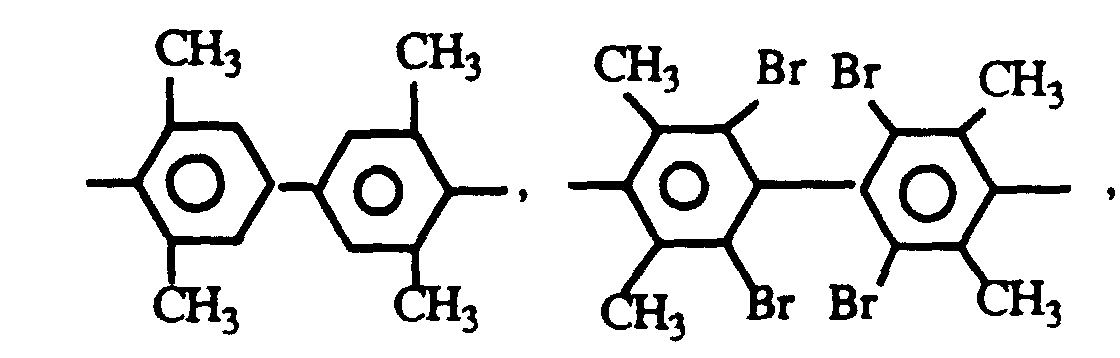
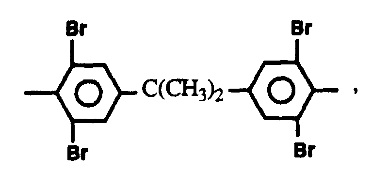
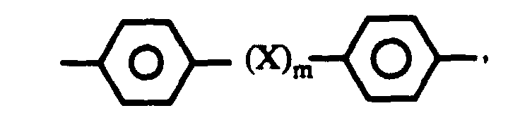
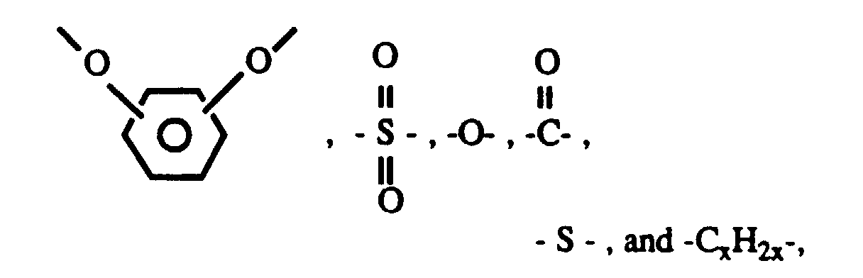
- Polyetherimides which can be utilized in the practice of the present invention to make the plasticized polyetherimide adhesive composition comprise the reaction product of substantially equal molar amounts of an aromatic bis(ether anhydride) of the formula, and an aryldiamine of the formula, NH 2 R 1 NH 2 , where R is a member selected from the class consisting of divalent organic radicals of the formulas, and and divalent organic radicals included within the formula, where X is a member selected from the class consisting of divalent radicals of the formulas, m is O or l, y is an integer equal to 1 to 5, and the bonds of the -O-R-O- radical of formula 1 are equally situated on the phthalic anhydride end groups in the ,3,3'-positions, 3,4'-positions or the ,4,4'-positions.
- the aromatic (ether anhydride) of formula (1) such as 2,2-bis[4-2,3-dicarboxyphenoxy)phenyl]propane dianhydride, and 2,2-bis[4(3,4-dicarboxyphenoxy)phenyl]propane dianhydride.
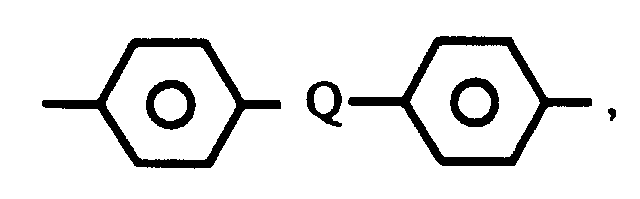
- R 1 in formula (2) is a divalent organic radical having from 6-20 carbon atoms and halogenated derivatives thereof, alkylene radicals and cycloalkylene radicals having from 2-20 carbon atoms, C (2-8) alkylene terminated polydiorganosiloxane, and divalent radicals included within the formula, where Q is a member selected from the class consisting of where x is an integer equal to 1 to 5.
- aryl diamines of formula (2) which also include mixtures thereof, there are, for example,
- Plasticizers which can be used in combination with the above-described polyetherimide are for example, pentaerythritol tetrabenzoate, triphenylphosphate and bisimides such as, bisphenol A dianhydride bis(N-phenylimide), bisphenol A dianhydride bis(N-methylimide), and bisphenol A dianhydride bis(N-butylimide), and bisphenol A dianhydride bis(N-pyridylimide),
- the plasticized polyetherimide can be made by solvent blending or melt blending procedures.
- a typical solvent blending procedure would involve the use of predetermined quantities of polyetherimide and plasticizer which are placed in a container with the appropriate amount of an organic solvent to dissolve the polymer and plasticizer and provide a clear homogeneous polymer solution. This can be accomplished by heating the mixture to about 80°C with gentle agitation. Suitable organic solvents are anisole, acetophenone, N-methylpyrrolidone, methylene chloride, chloroform, dimethylacetamide and p-methylacetophenone.
- the solution of plasticized polyetherimide can then be applied as an adhesive coating to the surface of a dielectric film, such as Kapton polyimide.
- An alternative to solution blending is melt blending.
- a polyetherimide, such as Ultem polyetherimide is heated above its melt flow temperature and an appropriate amount of plasticizer is added to the melt. In this manner, it is possible to extrude films for subsequent use as laminating adhesive
- the plasticized polyetherimide composition can be used as an adhesive in the fabrication of multi-chip integrated circuit arrays.
- the preferred method for assembling the integrated circuit array is shown by Eichelberger et al, U.S. Patent 4,783,695 which is incorporated herein by reference. Accordingly, a plurality of circuit chips is disposed on a substrate.
- the plasticized polyetherimide is applied onto the chips and the substrate in order that the resulting polyimide overlay layer bridges the chips.
- Application of the plasticized polyetherimide can be achieved by initially applying a solution of the plasticized polyetherimide by a spinning technique, or it can be heat pressed on in the form of a film or laminated on as a composite layer with a polyimide, such as a Kapton polyimide.
- Lamination may be achieved using conventional laminators employing a silicone rubber press pad to accomodate the surface topography of the circuitry.
- laminations can be achieved using a vacuum-pressure laminator. Lamination is conducted at the temperature at which the plasticized polyetherimide melts, preferably in the range between 200°C to 260°C.
- Via holes formed in the array resulting from the above processing steps can be used to provide contact to power, ground, or signal, or packaging pins if desired.
- an argon ion laser operating at 351 nm is used to drill vias through the Kapton polyimide and adhesive layer overlying the bond pads on the chips and substrate.
- a laser is sequentially focused at each pad site to ablate polymeric material.
- the polymer overlay film absorbs incident radiation which locally heats the film resulting in rapid thermal decomposition and evaporation.
- via holes can be formed by depositing a thin layer of metal, such as, for example, a 1000 ⁇ thick layer of titanium or chromium on the laminate surface. Openings in the metal are then patterned using conventional photolithography methods.
- the perforated metallic layer is then exposed to a laser beam to form through holes by ablation of the polymer film.
- An excimer laser or CW laser can be used in this process as well as reactive ion etching.
- the drawing shows in cross-section, a simplified view of a high density interconnect structure comprising a substrate to which there is affixed an integrated circuit chip having an interconnection pad, a dielectric overlay layer and a metal layer.
- a substrate such as alumina
- an IC chip at 30 which is bonded to the base of a well or recess in the substrate 10 by an epoxy chip adhesive at 20, such as Ablebond 84-1-LMN-T of Able Stik Lab., Gardena, CA..
- the well walls of substrate 10 are shown at 11 and 12.
- a plasticized polyetherimide adhesive layer at 40 which bonds a dielectric overlay layer 50, such as Kapton polyetherimide, to the substrate and IC chip.
- a metal layer for example, Ti/Cu/Ti, is shown at 60 having a via opening to a metal bond pad at 31 on the IC chip.
- the high density interconnect circuit arrays included within the scope of the present invention also can have one or more chips, and additional laminate layers above the laminate layers in direct contact with the IC chips and substrate.
- These additional laminated dielectric overlay layers can consist of a Kapton polyimide dielectric layer and an adhesive layer, such as a siloxane polyetherimide.
- a plurality of via openings to provide additional interconnection pads on IC chips and metal pads on the substrate are also within the scope of the present invention to provide more complex structures.
- a solution was prepared of 2.5 g of Ultem 1010 polyetherimide of the Plastics Division of GE Co.,0.25 g of Benzoflex S-552, a pentaerythritol tetrabenzoate ester of the Velsicol Chemical Co, 7.5 g of anisole and 0.8 g of toluene. The solution was then heated for several hours with stirring at 80°C. The solution was spin coated into a 1 mil thick metal frame supported Kapton polyimide film of the E.I. Dupont de Nemours Co. The resulting coated polyimide film was baked to remove the solvent.
- the bake cycle was 30 min at 110°C, 30 min at 150°C and 30 min at 175°C, followed by a final bake-out of 1 hr at 250°C.
- the polyimide/plasticized polyetherimide composite was then laminated to an alumina substrate having IC chips bonded on the alumina substrate within chip wells.
- the alumina substrate was placed in a vacuum chamber with the polyimide/polyetherimide composite film above with the plasticized polyetherimide side down overlying the chips and substrate.
- the chamber was evacuated and heated to 260°C.
- a pressure of 55 psi was applied to the top side of the polyimide/plasticized polyetherimide composite and the chamber held at this temperature for 1 hr.
- After cooling under pressure to a temperature below 150°C the laminated part was removed.
- a clean, void-free lamination resulted.
- a pull strength test on the laminated part resulted in the Kapton polyimide layer ripping at 7 lbs, whereas a lb pull strength was obtained with a laminate having a similar thickness of Kapton polyimide and polyetherimide free of plasticizer.
- Polymer solutions containing 0, 10, 20, 30 and 40% by weight Benzoflex S-552 in Ultem 1010 polyetherimide were prepared by dissolving the polymer and plasticizer in an appropriate amount of anisole.
- the polymer solutions were then respectively spun onto Kapton polyimide films supported on metal frames.
- the resulting coated polyimide films were then spin coated and baked to remove solvent. The bake cycle was identical to that described in example 1.
- the resulting composite structures contained 1/2 mil adhesives on 1 mil thick Kapton polyimide film.
- the resulting polyimide/plasticized polyetherimide composite layers were then laminated as described in example 1.
- the laminations were evaluated for optical quality. Excellent void free laminations were obtained.
- the unplasticized polyetherimide composite however, had numerous air pockets due to poor flow properties during lamination.
- a polymer solution was prepared by mixing 9 g of Ultem 1000 polyetherimide with 1 g of bisphenol A dianhydride bis(N-methylimide) in 40 g of anisole and heating for several hrs. at 80°C. The resulting solution was spin coated and baked to form a 1/2 mil adhesive film on Kapton polyimide. The resulting polyimide/plasticized polyetherimide composite was then laminated to an alumina substrate containing IC chips which had been placed in chip wells on the alumina substrate. The lamination was carried out as described in example 1 resulting in a void free lamination. A 7 lb pull strength test was performed before the Kapton polyimide showed signs of tearing apart.
- a plasticized polyetherimide layer (1/2 mil thick) was prepared by blending 5% by weight of bisphenol A dianhydride bis(N-phenylimide) with Ultem 1010 polyetherimide. The ingredients were dissolved in acetophenone to provide a clear solution which was used to form a solvent free layer.
- a composite Kapton polyimide/plasticized polyetherimide film was prepared which was laminated onto an alumina substrate at 250°C using a pressure of 45 psi applied to the top side.
- a pull strength test showed a value of 6.4 lbs. whereas a part laminated with unplasticized Ultem 1010 polyetherimide had a pull strength of 1.6 lbs.
- a polyimide/plasticized polyetherimide composite was prepared as described in example 1, except that the adhesive was applied to Kapton polyimide E film.
- the composite was then laminated to an aluminum nitride substrate containing IC chips composed of silicon and gallium arsenide. Lamination was accomplished by placing the composite and the substrate in a vacuum chamber having the plasticized polyetherimide side in contact with the chips and substrate. The chamber was evacuated. The array was heated to 2500° C with a pressure of 10 psi applied to the top side. These conditions were maintained for 20 min. After cooling under pressure to a temperature below 150°C, the laminated part was removed. A clean, void free lamination resulted.
- plasticizers can be used in conjunction with additional polyetherimides as shown in the description preceding these examples.
- One such series of plasticizers are commercially available from Velsicol Chemical, namely aromatic aliphatic ester derivatives of pentaerythritol.
- Some of the key requirements of the plasticizers are compatibility with polyetherimides and solvents and thermal stability in excess of 260°C.
Landscapes
- Chemical & Material Sciences (AREA)
- Chemical Kinetics & Catalysis (AREA)
- Organic Chemistry (AREA)
- Health & Medical Sciences (AREA)
- Medicinal Chemistry (AREA)
- Polymers & Plastics (AREA)
- Laminated Bodies (AREA)
- Adhesives Or Adhesive Processes (AREA)
- Die Bonding (AREA)
Description



bisphenol A dianhydride bis(N-phenylimide),


| PERFORMANCE SUMMARY OF PLASTICIZED POLYETHERIMIDE LAMINATIONS (260°C) | |||
| wt.% Benzoflex S-552 in Ultem 1010 | Lamination Quality | Electrical test | Remarks |
| 0 | poor (air bubbles) | - | |
| 10 | excellent, clear, void free | 100% functional | |
| 20 | excellent, clear void free | 100% functional | |
| 30 | excellent, clear void free | some opens | flow of plasticized polyetherimide during upper layer lamination at 185° |
| 40 | excellent, clear void free | some opens | flow of plasticized polyetherimide during upper layer lamination at 185°C |
Claims (11)
- A plasticized polyetherimide adhesive composition having a melt viscosity capable of providing substantially void free adhesive bonding at temperatures in the range of about 2000 to 260°C between overlay dielectric layer and substrate having at least one IC chip attached thereon, which plasticized polyetherimide composition consists of by by weight,(A) 100 parts of a polyetherimide, and(B) 5 to 25 parts of plasticizer.
- A plasticized polyetherimide adhesive in accordance with claim 1, where the plasticizer is a bisphenol A dianhydride bis(alkyl or aryl bisimide).
- A plasticized polyetherimide adhesive in accordance with claim 1, where the plasticizer is pentaerythritol tetrabenzoate.
- A plasticized polyetherimide adhesive in accordance with claim 1, where the plasticizer is triphenylphosphate.
- A plasticized polyetherimide adhesive in accordance with claim 2, where the plasticizer is bisphenol A dianhydride bis(N-phenylimide).
- A plasticized polyetherimide adhesive in accordance with claim 2, where the plasticizer is bisphenol A dianhydride bis(N-methylimide).
- A plasticized polyetherimide adhesive in accordance with claim 2, where the plasticizer is bisphenol A dianhydride bis(N-butylimide).
- A plasticized polyetherimide adhesive in accordance with claim 2, where the plasticizer is bisphenol A dianhydride bis(N-pyridylimide).
- A high density interconnect circuit array comprising,where the laminate layer of (c) has a plurality of via openings, where at least one of the via openings is aligned with at least one of the interconnection pads of (b) and a pattern of interconnection conductors disposed on top of the laminate layer so as to extend between some of the openings to provide electrical connections between at least one of the interconnection pads through the openings, which laminate layer of (c) comprises a dielectric overlay layer and an adhesive layer in direct contact with the integrated chip, which adhesive layer comprises a plasticized polyetherimide of any preceding claim having a melt viscosity sufficiently low to provide void free adhesive bonding at temperatures in the range of between 200°C to 260°C between the dielectric overlay layer and substrate having at least one integrated circuit chip disposed thereon.(a) a substrate,(b) at least one integrated circuit chip with at least one interconnection pad disposed on the substrate, and(c) a laminate layer overlying and bridging the integrated circuit chip,
- A high density interconnect circuit array in accordance with claim 9, having at least one additional laminate layer above the laminate layer of (c) comprising a dielectric layer and an adhesive layer.
- A high density interconnect circuit array in accordance with claim 10, where the dielectric layer is a polyimide and the adhesive layer is a siloxane polyimide.
Applications Claiming Priority (2)
| Application Number | Priority Date | Filing Date | Title |
|---|---|---|---|
| US07/987,849 US5300812A (en) | 1992-12-09 | 1992-12-09 | Plasticized polyetherimide adhesive composition and usage |
| US987849 | 1992-12-09 |
Publications (3)
| Publication Number | Publication Date |
|---|---|
| EP0604038A2 EP0604038A2 (en) | 1994-06-29 |
| EP0604038A3 EP0604038A3 (en) | 1995-01-04 |
| EP0604038B1 true EP0604038B1 (en) | 1999-08-04 |
Family
ID=25533624
Family Applications (1)
| Application Number | Title | Priority Date | Filing Date |
|---|---|---|---|
| EP93309664A Expired - Lifetime EP0604038B1 (en) | 1992-12-09 | 1993-12-02 | Plasticized polyetherimide adhesive compositions |
Country Status (4)
| Country | Link |
|---|---|
| US (1) | US5300812A (en) |
| EP (1) | EP0604038B1 (en) |
| JP (1) | JPH06256750A (en) |
| DE (1) | DE69325881T2 (en) |
Families Citing this family (23)
| Publication number | Priority date | Publication date | Assignee | Title |
|---|---|---|---|---|
| US5300813A (en) * | 1992-02-26 | 1994-04-05 | International Business Machines Corporation | Refractory metal capped low resistivity metal conductor lines and vias |
| US5418687A (en) * | 1994-02-01 | 1995-05-23 | Hewlett-Packard Company | Wafer scale multi-chip module |
| US5561085A (en) | 1994-12-19 | 1996-10-01 | Martin Marietta Corporation | Structure for protecting air bridges on semiconductor chips from damage |
| US5866952A (en) * | 1995-11-30 | 1999-02-02 | Lockheed Martin Corporation | High density interconnected circuit module with a compliant layer as part of a stress-reducing molded substrate |
| JP2842378B2 (en) * | 1996-05-31 | 1999-01-06 | 日本電気株式会社 | High-density mounting structure for electronic circuit boards |
| US5972145A (en) * | 1996-06-07 | 1999-10-26 | International Business Machines Corporation | Removable passivating polyimide coating and methods of use |
| US5879787A (en) * | 1996-11-08 | 1999-03-09 | W. L. Gore & Associates, Inc. | Method and apparatus for improving wireability in chip modules |
| FR2766834B1 (en) * | 1997-07-29 | 1999-10-08 | Eurocopter France | ADHESIVE COMPOSITION FOR HOT GLUING AND GLUING PROCESS FOR IMPLEMENTING IT |
| US6856013B1 (en) * | 1999-02-19 | 2005-02-15 | Micron Technology, Inc. | Integrated circuit packages, ball-grid array integrated circuit packages and methods of packaging an integrated circuit |
| US6825550B2 (en) | 1999-09-02 | 2004-11-30 | Micron Technology, Inc. | Board-on-chip packages with conductive foil on the chip surface |
| US7042070B2 (en) * | 1999-09-22 | 2006-05-09 | Texas Instruments Incorporated | Direct attachment of semiconductor chip to organic substrate |
| US6571468B1 (en) * | 2001-02-26 | 2003-06-03 | Saturn Electronics & Engineering, Inc. | Traceless flip chip assembly and method |
| US7498196B2 (en) * | 2001-03-30 | 2009-03-03 | Megica Corporation | Structure and manufacturing method of chip scale package |
| US20030064542A1 (en) * | 2001-10-02 | 2003-04-03 | Corisis David J. | Methods of packaging an integrated circuit |
| TW584950B (en) | 2001-12-31 | 2004-04-21 | Megic Corp | Chip packaging structure and process thereof |
| TW544882B (en) * | 2001-12-31 | 2003-08-01 | Megic Corp | Chip package structure and process thereof |
| TW503496B (en) * | 2001-12-31 | 2002-09-21 | Megic Corp | Chip packaging structure and manufacturing process of the same |
| US6673698B1 (en) | 2002-01-19 | 2004-01-06 | Megic Corporation | Thin film semiconductor package utilizing a glass substrate with composite polymer/metal interconnect layers |
| US6964881B2 (en) * | 2002-08-27 | 2005-11-15 | Micron Technology, Inc. | Multi-chip wafer level system packages and methods of forming same |
| DE10253163B4 (en) * | 2002-11-14 | 2015-07-23 | Epcos Ag | Hermetic encapsulation device and wafer scale manufacturing method |
| US7220490B2 (en) | 2003-12-30 | 2007-05-22 | E. I. Du Pont De Nemours And Company | Polyimide based adhesive compositions useful in flexible circuit applications, and compositions and methods relating thereto |
| JP5306634B2 (en) * | 2007-11-22 | 2013-10-02 | 新光電気工業株式会社 | WIRING BOARD, SEMICONDUCTOR DEVICE, AND WIRING BOARD MANUFACTURING METHOD |
| US10240030B2 (en) * | 2014-12-02 | 2019-03-26 | Sabic Global Technologies B.V. | Article comprising a high flow polyetherimide composition |
Family Cites Families (9)
| Publication number | Priority date | Publication date | Assignee | Title |
|---|---|---|---|---|
| US5047487A (en) * | 1985-01-04 | 1991-09-10 | Raychem Corporation | Compositions of poly(imides) having phenylindane diamines and/or dianhydride moieties in the poly(imide) backbone |
| US4624724A (en) * | 1985-01-17 | 1986-11-25 | General Electric Company | Method of making integrated circuit silicon die composite having hot melt adhesive on its silicon base |
| FR2592050B1 (en) * | 1985-12-24 | 1988-01-08 | Centre Etd Mat Org Tech Avance | ARYLALIPHATIC COPOLYIMIDES WITH ETHER LINES, THEIR PREPARATION, THEIR MIXTURES OR REACTION PRODUCTS WITH EPOXIDE RESINS AND THEIR USE IN THE MANUFACTURE OF FLEXIBLE COMPOSITE MATERIALS |
| US4783695A (en) * | 1986-09-26 | 1988-11-08 | General Electric Company | Multichip integrated circuit packaging configuration and method |
| US4897153A (en) * | 1989-04-24 | 1990-01-30 | General Electric Company | Method of processing siloxane-polyimides for electronic packaging applications |
| CA2026201A1 (en) * | 1989-09-26 | 1991-03-27 | Kazuo Doyama | Engineering plastic composition and articles made of the same |
| DE3941280A1 (en) * | 1989-12-14 | 1991-06-20 | Basf Ag | POLYMER GRANULES WITH IMPROVED PROCESSABILITY |
| US5161093A (en) * | 1990-07-02 | 1992-11-03 | General Electric Company | Multiple lamination high density interconnect process and structure employing a variable crosslinking adhesive |
| US5095060A (en) * | 1990-12-19 | 1992-03-10 | General Electric Company | Blends of polyphenylene ether resin, a polyetherimide siloxane copolymer and pentaerythritol tetrabenzoate |
-
1992
- 1992-12-09 US US07/987,849 patent/US5300812A/en not_active Expired - Lifetime
-
1993
- 1993-12-02 DE DE69325881T patent/DE69325881T2/en not_active Expired - Fee Related
- 1993-12-02 EP EP93309664A patent/EP0604038B1/en not_active Expired - Lifetime
- 1993-12-08 JP JP5307607A patent/JPH06256750A/en active Pending
Also Published As
| Publication number | Publication date |
|---|---|
| EP0604038A3 (en) | 1995-01-04 |
| DE69325881T2 (en) | 2000-02-24 |
| US5300812A (en) | 1994-04-05 |
| EP0604038A2 (en) | 1994-06-29 |
| DE69325881D1 (en) | 1999-09-09 |
| JPH06256750A (en) | 1994-09-13 |
Similar Documents
| Publication | Publication Date | Title |
|---|---|---|
| US5300812A (en) | Plasticized polyetherimide adhesive composition and usage | |
| CN102167905B (en) | Polyimide resin composition for semiconductor devices and the film formation method in using its semiconductor device and semiconductor device | |
| CN107325285B (en) | Polyimide, polyimide-based adhesive, adhesive material, adhesive layer, adhesive sheet, laminate, wiring board, and method for producing same | |
| US6329050B1 (en) | Adhesive for electronic parts and adhesive tape for electronic parts | |
| WO2020219852A1 (en) | Phenolic functionalized polyimides and compositions thereof | |
| WO2007018120A1 (en) | Adhesive film and semiconductor device using same | |
| JPH04262593A (en) | Multilayer interconnection structure and multilayers laminating method therefor | |
| JPH08325533A (en) | Adhesive tape for electronic parts and liquid adhesive | |
| US20070004844A1 (en) | Dielectric material | |
| JP5293496B2 (en) | Adhesive composition, adhesive film, and semiconductor device | |
| CN120513511A (en) | Method for producing laminate, and resin composition | |
| US5534602A (en) | High temperature polyether imide compositions and method for making | |
| JP3055388B2 (en) | Adhesive film | |
| EP0618269B1 (en) | Thermosetting resin compositions and their use for making resin articles and thin film wiring boards | |
| EP0015720B1 (en) | Copolymeric coating compositions | |
| CN110117418A (en) | The production method of cover film and the insulating layer of semiconductor component surfaces | |
| JP4071958B2 (en) | Polyimide resin composition | |
| JP4940499B2 (en) | Low dielectric constant polymer | |
| JP2025532030A (en) | Polyimide adhesive compositions containing maleimide moieties and amine compounds, components and methods | |
| WO2023228815A1 (en) | Resin composition, cured product, antenna element and electronic component | |
| EP1420048A2 (en) | Metal laminate | |
| JPH0532891A (en) | Thermosetting resin composition and printed wiring board using the same | |
| JP3536640B2 (en) | Adhesive film, manufacturing method thereof, support member with adhesive film, and semiconductor device | |
| JP3570202B2 (en) | Adhesive film, manufacturing method thereof, support member with adhesive film, and semiconductor device | |
| KR102411810B1 (en) | Semiconductor package |
Legal Events
| Date | Code | Title | Description |
|---|---|---|---|
| PUAI | Public reference made under article 153(3) epc to a published international application that has entered the european phase |
Free format text: ORIGINAL CODE: 0009012 |
|
| AK | Designated contracting states |
Kind code of ref document: A2 Designated state(s): DE FR GB IT NL |
|
| PUAL | Search report despatched |
Free format text: ORIGINAL CODE: 0009013 |
|
| AK | Designated contracting states |
Kind code of ref document: A3 Designated state(s): DE FR GB IT NL |
|
| 17P | Request for examination filed |
Effective date: 19950704 |
|
| 17Q | First examination report despatched |
Effective date: 19961112 |
|
| GRAG | Despatch of communication of intention to grant |
Free format text: ORIGINAL CODE: EPIDOS AGRA |
|
| GRAG | Despatch of communication of intention to grant |
Free format text: ORIGINAL CODE: EPIDOS AGRA |
|
| GRAH | Despatch of communication of intention to grant a patent |
Free format text: ORIGINAL CODE: EPIDOS IGRA |
|
| GRAH | Despatch of communication of intention to grant a patent |
Free format text: ORIGINAL CODE: EPIDOS IGRA |
|
| GRAA | (expected) grant |
Free format text: ORIGINAL CODE: 0009210 |
|
| AK | Designated contracting states |
Kind code of ref document: B1 Designated state(s): DE FR GB IT NL |
|
| REF | Corresponds to: |
Ref document number: 69325881 Country of ref document: DE Date of ref document: 19990909 |
|
| ET | Fr: translation filed | ||
| ITF | It: translation for a ep patent filed | ||
| PLBE | No opposition filed within time limit |
Free format text: ORIGINAL CODE: 0009261 |
|
| STAA | Information on the status of an ep patent application or granted ep patent |
Free format text: STATUS: NO OPPOSITION FILED WITHIN TIME LIMIT |
|
| 26N | No opposition filed | ||
| REG | Reference to a national code |
Ref country code: FR Ref legal event code: TP |
|
| REG | Reference to a national code |
Ref country code: GB Ref legal event code: 732E |
|
| NLS | Nl: assignments of ep-patents |
Owner name: LOCKHEED MARTIN CORPORATION |
|
| PGFP | Annual fee paid to national office [announced via postgrant information from national office to epo] |
Ref country code: NL Payment date: 20011120 Year of fee payment: 9 Ref country code: FR Payment date: 20011120 Year of fee payment: 9 |
|
| PGFP | Annual fee paid to national office [announced via postgrant information from national office to epo] |
Ref country code: GB Payment date: 20011122 Year of fee payment: 9 |
|
| PGFP | Annual fee paid to national office [announced via postgrant information from national office to epo] |
Ref country code: DE Payment date: 20011123 Year of fee payment: 9 |
|
| REG | Reference to a national code |
Ref country code: GB Ref legal event code: IF02 |
|
| PG25 | Lapsed in a contracting state [announced via postgrant information from national office to epo] |
Ref country code: GB Free format text: LAPSE BECAUSE OF NON-PAYMENT OF DUE FEES Effective date: 20021202 |
|
| PG25 | Lapsed in a contracting state [announced via postgrant information from national office to epo] |
Ref country code: NL Free format text: LAPSE BECAUSE OF NON-PAYMENT OF DUE FEES Effective date: 20030701 Ref country code: DE Free format text: LAPSE BECAUSE OF NON-PAYMENT OF DUE FEES Effective date: 20030701 |
|
| GBPC | Gb: european patent ceased through non-payment of renewal fee | ||
| NLV4 | Nl: lapsed or anulled due to non-payment of the annual fee |
Effective date: 20030701 |
|
| PG25 | Lapsed in a contracting state [announced via postgrant information from national office to epo] |
Ref country code: FR Free format text: LAPSE BECAUSE OF NON-PAYMENT OF DUE FEES Effective date: 20030901 |
|
| REG | Reference to a national code |
Ref country code: FR Ref legal event code: ST |
|
| PG25 | Lapsed in a contracting state [announced via postgrant information from national office to epo] |
Ref country code: IT Free format text: LAPSE BECAUSE OF NON-PAYMENT OF DUE FEES;WARNING: LAPSES OF ITALIAN PATENTS WITH EFFECTIVE DATE BEFORE 2007 MAY HAVE OCCURRED AT ANY TIME BEFORE 2007. THE CORRECT EFFECTIVE DATE MAY BE DIFFERENT FROM THE ONE RECORDED. Effective date: 20051202 |