EP0602888B1 - Performing arithmetic operations on data - Google Patents
Performing arithmetic operations on data Download PDFInfo
- Publication number
- EP0602888B1 EP0602888B1 EP93309863A EP93309863A EP0602888B1 EP 0602888 B1 EP0602888 B1 EP 0602888B1 EP 93309863 A EP93309863 A EP 93309863A EP 93309863 A EP93309863 A EP 93309863A EP 0602888 B1 EP0602888 B1 EP 0602888B1
- Authority
- EP
- European Patent Office
- Prior art keywords
- component
- bit
- data item
- component data
- circuitry
- Prior art date
- Legal status (The legal status is an assumption and is not a legal conclusion. Google has not performed a legal analysis and makes no representation as to the accuracy of the status listed.)
- Expired - Lifetime
Links
- 238000012545 processing Methods 0.000 claims description 79
- 239000002131 composite material Substances 0.000 claims description 48
- 238000000034 method Methods 0.000 claims description 38
- 238000010586 diagram Methods 0.000 description 7
- 238000003860 storage Methods 0.000 description 7
- 238000013500 data storage Methods 0.000 description 6
- 230000000295 complement effect Effects 0.000 description 4
- 238000012546 transfer Methods 0.000 description 4
- 230000000694 effects Effects 0.000 description 3
- 238000012937 correction Methods 0.000 description 2
- 238000010191 image analysis Methods 0.000 description 2
- 238000004519 manufacturing process Methods 0.000 description 2
- 230000003287 optical effect Effects 0.000 description 2
- 239000004065 semiconductor Substances 0.000 description 2
- 238000004088 simulation Methods 0.000 description 2
- 238000003892 spreading Methods 0.000 description 2
- 238000004458 analytical method Methods 0.000 description 1
- 238000013459 approach Methods 0.000 description 1
- 238000003491 array Methods 0.000 description 1
- 230000001419 dependent effect Effects 0.000 description 1
- 238000001514 detection method Methods 0.000 description 1
- 238000000605 extraction Methods 0.000 description 1
- 238000003702 image correction Methods 0.000 description 1
- 230000002452 interceptive effect Effects 0.000 description 1
- 230000003362 replicative effect Effects 0.000 description 1
- 238000012795 verification Methods 0.000 description 1
Images


Classifications
-
- G—PHYSICS
- G06—COMPUTING; CALCULATING OR COUNTING
- G06F—ELECTRIC DIGITAL DATA PROCESSING
- G06F7/00—Methods or arrangements for processing data by operating upon the order or content of the data handled
- G06F7/38—Methods or arrangements for performing computations using exclusively denominational number representation, e.g. using binary, ternary, decimal representation
- G06F7/48—Methods or arrangements for performing computations using exclusively denominational number representation, e.g. using binary, ternary, decimal representation using non-contact-making devices, e.g. tube, solid state device; using unspecified devices
- G06F7/50—Adding; Subtracting
- G06F7/505—Adding; Subtracting in bit-parallel fashion, i.e. having a different digit-handling circuit for each denomination
-
- G—PHYSICS
- G06—COMPUTING; CALCULATING OR COUNTING
- G06F—ELECTRIC DIGITAL DATA PROCESSING
- G06F7/00—Methods or arrangements for processing data by operating upon the order or content of the data handled
- G06F7/38—Methods or arrangements for performing computations using exclusively denominational number representation, e.g. using binary, ternary, decimal representation
- G06F7/48—Methods or arrangements for performing computations using exclusively denominational number representation, e.g. using binary, ternary, decimal representation using non-contact-making devices, e.g. tube, solid state device; using unspecified devices
-
- G—PHYSICS
- G06—COMPUTING; CALCULATING OR COUNTING
- G06F—ELECTRIC DIGITAL DATA PROCESSING
- G06F9/00—Arrangements for program control, e.g. control units
- G06F9/06—Arrangements for program control, e.g. control units using stored programs, i.e. using an internal store of processing equipment to receive or retain programs
- G06F9/30—Arrangements for executing machine instructions, e.g. instruction decode
- G06F9/30003—Arrangements for executing specific machine instructions
- G06F9/30007—Arrangements for executing specific machine instructions to perform operations on data operands
- G06F9/30036—Instructions to perform operations on packed data, e.g. vector, tile or matrix operations
-
- G—PHYSICS
- G06—COMPUTING; CALCULATING OR COUNTING
- G06F—ELECTRIC DIGITAL DATA PROCESSING
- G06F2207/00—Indexing scheme relating to methods or arrangements for processing data by operating upon the order or content of the data handled
- G06F2207/38—Indexing scheme relating to groups G06F7/38 - G06F7/575
- G06F2207/3804—Details
- G06F2207/3808—Details concerning the type of numbers or the way they are handled
- G06F2207/3828—Multigauge devices, i.e. capable of handling packed numbers without unpacking them
-
- G—PHYSICS
- G06—COMPUTING; CALCULATING OR COUNTING
- G06F—ELECTRIC DIGITAL DATA PROCESSING
- G06F2207/00—Indexing scheme relating to methods or arrangements for processing data by operating upon the order or content of the data handled
- G06F2207/38—Indexing scheme relating to groups G06F7/38 - G06F7/575
- G06F2207/3804—Details
- G06F2207/386—Special constructional features
Definitions
- the present invention relates to techniques for performing arithmetic operations on data.
- Wilson US-A 5,129,092 (“Wilson '092”), describes techniques for processing data matrices such as images and spatially related data using neighborhood processing units. As shown and described in relation to Figs. 1 and 2, the processing units form an array with several groups of eight processing units. Each processing unit's connections to its adjacent processing units to the immediate left and right in the array include a carry in line to its left and a carry out line to the right.
- Wilson '092 describes arithmetic operations beginning at col. 12 line 40.
- bit serial arithmetic a carry signal from a carry flip-flop is passed to multiplexers, one of which acts as a truth table for a carry propagate value, which is stored in flip-flops, provided to an output selector, and can be read back to memory.
- parallel arithmetic a carry input from a processing unit to the immediate left is obtained and a carry output propagates to a processing unit to the immediate right.
- FIG. 7 shows a Connection Machine system that performs image processing by simulating a binary image jungle (BIJ).
- a front end processor can make calls to cause processing units in the Connection Machine to perform arithmetic and logical operations.
- Fig. 8 illustrates a part of an array of processing units in a Connection Machine, with a processing unit storing a pixel value of an image at a lowest level of a BIJ and receiving a pixel value from another processing unit at the next higher level of the BIJ.
- each processing unit operates on the results from the next lower level of its first and second children.
- Figs. 13 and 14 each show a sequence of data item arrays in which sums of pixel values are obtained.
- each processing unit's local memory can contain a respective pixel's value.
- EP-A-0 464 601 discloses an arithmetic operation system in which a carry control indication register stores carry control information for each of a plurality of cascaded arithmetic units.
- Each arithmetic unit includes a carry controller that receives a carry control bit from the carry control indication register and, based on the carry control bit, modifies an output carry from the arithmetic unit before it is supplied to the adjacent more significant bit arithmetic unit.
- the system can be partitioned into fields at arbitrary positions.
- EP-A-0 486 143 discloses techniques for parallel processing of data in which, before processing, operands are packed into a word with at least one cleared buffer bit between each operand.
- the buffer bit is cleared before any arithmetic or logical operation involving signed arithmetic and again before evaluating results. This prevents propagation of a signed bit from flowing into bits of another operand's result.
- logic operations Some operations, referred to herein as "logic operations,” obtain one result bit using each operand bit. Therefore, a logic operation produces valid results when performed in parallel on a composite operand that includes a plurality of component data items. Examples include NOT, AND, OR, and XOR.
- ordinary arithmetic operations can obtain a result with more bits than the values on which the operations are performed. For example, adding two K-bit values can produce a (K + 1)-bit result because of a carry signal. Subtracting one K-bit value from another that is smaller can result in a borrow signal to the (K + 1)th bit. Multiplying two K-bit values can produce a 2K-bit result. And division can sometimes produce an unlimited number of bits if not truncated at some level of precision.
- each component could relate to a pixel of an image; the components can be gray scale or color pixel values.
- inter-component signals signals between components
- inter-component signals signals between components
- Some techniques use a processor with special circuitry that can prevent inter-component signals.
- Others which can use a conventional processor, obtain valid results of an arithmetic operations despite inter-component signals.
- the article includes a data storage medium and instruction data stored by the data storage medium, which could be a magnetic storage medium, an optical storage medium, a semiconductor memory, or other memory medium.
- the article can be used in a system that includes memory, a storage medium access device, and a processor.
- the memory stores multi-bit data items, such as data relating to pixels of an image.
- the instruction data indicate instructions a processor can execute to perform an arithmetic operation in parallel on a composite operand that includes more than one of the multi-bit data items.
- the instructions ensure that the results obtained are valid despite inter-component signals.
- the instruction data can be, for example, code that can be executed by a microprocessor such as the CPU of a conventional workstation or other computer.
- One special circuitry technique uses a processor with gating circuitry that can be used to control transfer of signals between component data items. This technique can use conventional microprocessors if the maximum component width is an integer multiple of the microprocessor width.
- Another special circuitry technique uses a processor with a mask register connected to the processing circuitry.
- the mask register could be loaded with an allow value, such as ON, in bit positions that are allowed to receive inter-component signals from the next lower bit positions.
- the mask register could be loaded with a prevent value, such as OFF, in bit positions that are not allowed to receive inter-component signals from the next lower bit positions.
- the mask register could be loaded each time component width changes, allowing many component widths. Also, for operations on data other than composite operands, the mask register can be loaded with values that permit inter-component signals to propagate freely.
- One technique that can use a conventional processor uses one or more buffer bits between each pair of adjacent component data items. For example, a buffer bit could be annexed to every component, above its most significant bit or below its least significant bit. Or, if precision can be sacrificed, the least significant bit of each component could be a buffer bit. The values of the buffer bits can then be manipulated to prevent or compensate for inter-component signals.
- An addition operation can clear all buffer bits before adding composite operands. For example, if the operation adds pairs of components, each composite operand can be ANDed with a mask having an OFF value in each buffer bit and an ON value elsewhere. If the operation adds a constant to every component, a constant operand can be formed by replicating the constant separated by buffer bits that have an OFF value.
- a subtraction operation can use a buffer bit above each component's most significant bit.
- each buffer bit in a composite minuend can have ON values and each buffer bit in a composite subtrahend can start with an OFF value.
- the buffer bits ensure that each component of the minuend has a value exceeding the aligned component of the subtrahend. As a result, a borrow signal cannot propagate to the next component's result.
- Multiplication and division can be implemented with addition and subtraction, together with shifting and logic operations using masks.
- the buffer bits can be used to generate the masks.
- the buffer bit technique can also be implemented using special circuitry that inserts buffer bits between component data items.
- Another technique that can use a conventional processor can be used to reduce or eliminate buffer bits for certain arithmetic operations.
- This technique prepares composite operands for an addition operation by adjusting values indicated by component data items. For example, if it can be predicted that a certain component's value will cause an inter-component carry signal, the component adjacent its most significant bit can be adjusted by subtracting one from it prior to the operation, so that the inter-component carry signal has no effect.
- the techniques of the invention are advantageous because they provide a range of alternatives, each of which is useful in appropriate situations.
- Each technique can ensure that inter-component signals do not invalidate results of an arithmetic operation performed in parallel on composite operands with plural multi-bit component data items such as pixel values.
- some of the techniques can be used together in certain situations. As a result of the invention, arithmetic operations on multi-bit component data items can be performed rapidly and efficiently in many situations.
- composite operand used below is an operand that includes two or more data items, referred to as “component data items” or “components.”
- a processor or other circuitry performing an arithmetic operation on a composite operand may produce an "inter-component signal."
- An inter-component signal is a signal like a carry signal, a borrow signal, or a shifted bit that may cause an operation on one component to affect results obtained for another component.
- An arithmetic operation "would ordinarily produce an inter-component signal from a component data item" if the operation performed according to ordinary arithmetic produces an inter-component signal whose effect extends outside the component data item. Adding one to a two-bit component data item with the value 11, for example, would ordinarily produce an inter-component carry signal affecting the next bit to the left.
- Figs. 1-4 illustrate general features of the invention.
- Fig. 1 shows schematically a technique that obtains a valid result of an arithmetic operation performed in parallel on multi-bit component data items.
- Fig. 2 shows a software product with instruction data indicating instructions a processor can perform in accordance with a technique like that in Fig. 1.
- Fig. 3 shows general features of a processor with inter-component prevent circuitry to prevent transfer of inter-component signals between processing positions.
- Fig. 4 shows general acts in a method of operating a processor to obtain valid results despite an inter-component signal.
- composite operand 10 includes component data items 12 and 14, each including two bits.
- Component 12 has the value 01
- component 14 has the value 10.
- composite operand 20 includes components 22 and 24, with the respective values 01 and 10.
- Components 12 and 22 can occupy the same bit positions and components 14 and 24 similarly can occupy the same bit positions
- the most significant bits of components 12 and 22 can be adjacent respectively to the least significant bits of components 12 and 22. Therefore, when a processor performs an arithmetic operation adding operand 10 to operand 20, components 12 and 22 are added and components 14 and 24 are added.
- result 30 includes data items 32 and 34, with the values 11 and 00 respectively.
- the "1" values in data item 32 both result from carry signals, carry signal 36 from the most significant bit of components 14 and 24 and carry signal 38 from the least significant bit of components 12 and 22.
- carry signal 36 causes an invalid result in data item 32, because the sum of 01 and 01 is 10, not 11.
- the processor can instead produce valid result 40, in which data items 42 and 44 have the values 10 and 00 respectively.
- valid result 40 in which data items 42 and 44 have the values 10 and 00 respectively.
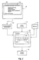
- Fig. 2 shows software product 60, an article of manufacture that can be used in a system that includes components like those shown in Fig. 2.
- Software product 60 includes data storage medium 62 that can be accessed by storage medium access device 64.
- Data storage medium 62 could, for example, be a magnetic medium such as a set of one or more floppy disks, an optical medium such as a set of one or more CD-ROMs, semiconductor memory, or any other appropriate medium for storing data.
- Data storage medium 62 stores data that storage medium access device 64 can provide to processor 66, which could for example be a microprocessor.
- Processor 66 is connected for receiving data from input circuitry 70.
- the data could be obtained from any appropriate source, such as a facsimile (fax) machine; a scanner, which could be the scanner of a digital copier or an input/output device of a computer; an editor, which could be a forms editor or other interactive image editor controlled by user input devices such as a keyboard and mouse or a pen- or stylus-based input device; or a network, which could be a local area network or other network capable of transmitting data.
- the data could relate to an image.
- Processor 66 is also connected for providing data to output circuitry 80.
- the data could in turn be provided to a fax machine, a printer, a display, or a network.
- the printer could be the printer of a digital copier or an input/output device of a computer.
- software product 60 includes data stored by storage medium 62.
- the stored data include instruction data indicating arithmetic operation instructions 90.
- Processor 66 can execute instructions 90 to perform an arithmetic operation on a composite operand that includes a plurality of component data items.
- Processor 66 can obtain the component data items on which the arithmetic operation is performed by accessing memory 92.
- Each item of data can, for example, relate to a pixel of an image.
- the items of data can each include more than one bit.
- the data stored by storage medium 62 could also include data indicating instructions processor 66 can execute to store data items received from input circuitry 70 in memory 92, to retrieve data items from memory 92 for an arithmetic operation or to be provided to output circuitry 80, or to store data items resulting from an arithmetic operation in memory 92.
- Processor 66 includes processing circuitry 94 with plural processing positions 96.
- Processor 66 could, for example, be a conventional microprocessor.
- Each of processing positions 96 can perform an operation on one bit.
- Processing circuitry 94 includes position connecting circuitry 98 connecting processing positions 96 in pairs to form an array. A signal from one processing position in a pair can be transferred by position connecting circuitry 98 to the other processing unit.
- Each component data item in a composite operand on which an arithmetic operation is being performed can be in a respective subarray of processing positions 96.
- Processor 66 can execute arithmetic operation instructions 90 to obtain a resulting data item in each component's subarray.
- the subarray of a first component provides an inter-component signal to position connecting circuitry 98.
- the inter-component signal is capable of causing the arithmetic operation to obtain a resulting data item indicating an invalid result in the subarray of a second component.
- Processor 66 in executing arithmetic operation instructions 90, acts to ensure that the resulting data item in the second component's subarray indicates a valid result of the arithmetic operation on the second component, despite the inter-component signal.
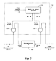
- Fig. 3 shows general components of a processor 100.
- Processing circuitry 102 can perform arithmetic operations in parallel on composite operands. Like processing circuitry 94 in Fig. 2, processing circuitry 102 has plural processing positions 104. Each of processing positions 104 can perform an operation on one bit.
- Processing circuitry 102 includes position connecting circuitry 106 connecting processing positions 104 in pairs to form an array. A signal from one processing position in a pair can be transferred by position connecting circuitry 106 to the other processing unit.
- Inter-component prevent circuitry 110 is connected so that it can prevent transfer of signals between processing positions 104 through position connecting circuitry 106.
- Control circuitry 112 is connected to provide control signals to processing circuitry 102 and inter-component prevent circuitry 110.
- the control signals cause processing circuitry 102 to perform an arithmetic operation in parallel on a composite operand that includes plural multi-bit component data items.
- each component data item can relate to a pixel of an image.
- Each component is in a respective subarray of processing positions 104.
- Processing circuitry 102 performs the arithmetic operation on each component to obtain a resulting data item in each component's subarray.
- the subarray of a first component provides an inter-component signal to position connecting circuitry 106.
- the inter-component signal is capable of causing the arithmetic operation to obtain a resulting data item indicating an invalid result in the subarray of a second component.
- control signals also cause inter-component prevent circuitry 110 to prevent transfer of the inter-component signal by position connecting circuitry 106.
- inter-component prevent circuitry 110 causes transfer of the inter-component signal by position connecting circuitry 106.
- Fig. 4 shows general acts in a method of operating a processor with processing circuitry like processing circuitry 94 in Fig. 2.
- the act in box 130 provides a composite operand to processing circuitry 94, with each component being provided to a respective subarray of processing positions 96.
- the act in box 132 operates processing circuitry 94 to perform an arithmetic operation in parallel on the composite operand to obtain a resulting data item in each subarray.
- the subarray of a first component provides an inter-component signal.
- the act in box 132 is performed so as to ensure that each resulting data item indicates a valid result despite the inter-component signal.
- Figs. 5 and 6 illustrate two implementations of the general components shown in Fig. 3.
- Figs. 7 and 8 illustrate two implementations of the general steps shown in Fig. 4 that are applicable for processing units that can operate in parallel on more than one data item; a number of such processing units could be used in parallel without position connecting circuitry between them.
- Fig. 5 illustrates an implementation of the general components described in relation to Fig. 3 that can employ conventional microprocessors in processing circuitry 102.
- the implementation in Fig. 5 includes inter-component prevent circuitry 110 that can prevent an inter-component signal between the microprocessors. Therefore, if each microprocessor is M bits wide, where M ⁇ 1, the array of processing positions can be divided into subarrays at any integer multiple of M bits. Each subarray can then perform arithmetic operations on component data items.
- Fig. 5 shows microprocessor 150, the pth microprocessor in an array of microprocessors that provides processing positions 104.
- position connecting circuitry 106 connects the carry in and carry out leads of adjacent microprocessors.
- the carry in lead of microprocessor 150 receives a signal from the carry out lead of the ( p - 1)th microprocessor only if a carry select signal is provided to AND gate 152.
- a signal from the carry out lead of microprocessor 150 is provided to the ( p + 1)th microprocessor only if a carry select signal is provided to AND gate 154.
- Width-to-select decoder 156 can be a read only memory (ROM), programmable array logic (PAL), or other conventional circuitry that responds to a signal from control circuitry 112 by providing carry enable signals to the appropriate AND gates so that carry signals can be transferred within a subarray but not between subarrays of different component data items.
- the signal from control circuitry 112 can indicate a subarray width, such as M, 2M, 3M, and so forth, and the output from width-to-select decoder 156 can accordingly be ON for AND gates within a subarray and OFF for AND gates between subarrays.
- the signal from control circuitry 112 can indicate a width such that the output from width-to-select decoder 156 provides an ON output to all AND gates.
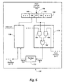
- Fig. 6 illustrates another implementation of the general components described in relation to Fig. 3 that can employ a customized arithmetic logic unit (ALU) 170.
- the implementation in Fig. 6 includes inter-component prevent circuitry that can prevent an inter-component signal between any two adjacent processing positions within ALU 170. Therefore, if ALU 170 is M bits wide, the array of processing positions can be divided into equal subarrays at any integer factor of M bits. Each subarray can then perform arithmetic operations on component data items.
- ALU arithmetic logic unit
- Processing position 172 is the pth position in processing positions 104 within ALU 170.
- position connecting circuitry as in Fig. 3 connects carry in and carry out leads of adjacent processing positions. As shown, however, the carry in lead of position 172 receives a signal from the carry out lead of the ( p - 1)th position through position connecting logic 174. Similarly, the carry out lead of position 172 provides a signal to the carry in lead of the ( p + 1)th position through position connecting logic 176.
- Position connecting logic 174 provides a carry in signal from the ( p - 1)th position only if an ON value is provided to the other input lead of AND gate 180, so that the signal is provided to the carry in lead of position 172 through OR gate 182.
- the mask register provides an OFF signal to AND gates 180 and 184, the carry in lead of position 172 receives an ON signal only if the subtract signal to AND gate 184 is ON.
- Position connecting logic 176 includes similar circuitry.
- Mask register 190 can be implemented with conventional register circuitry that can be loaded with mask values by signals from control circuitry 112.
- the mask values include enable values, illustratively ON, and prevent values, illustratively OFF.
- Mask register 190 is connected so that each mask value is provided to AND gates that control the carry in line of a respective position like AND gates 180 and 184.
- Mask value 192 controls the carry in line of the (p - 1)th position, mask value 194 the carry in line of the p th position, and mask value 196 the carry in line of the ( p + 1)th position.
- an enable value allows a carry out signal from the next lower position to propagate upward, while a prevent value prevents upward propagation of carry out signals. But during a subtraction operation, a prevent value provides a carry in signal even if the next lower position is not providing a carry out signal, as required by the standard implementation of two's complement arithmetic.
- Control circuitry 112 can load mask register 190 each time the number of bits in each component data item changes. For instance, if the component data items are pixel values, mask values can be changed whenever the number of bits in each pixel value changes.
- mask value 192 controls the uppermost processing position of one component's subarray
- mask value 194 controls the lowermost processing position of an adjacent component's subarray, which is position 172.
- Each of the above implementations employs special circuitry.
- the following implementations do not require special circuitry, but may use processing positions less efficiently than the above implementations due to additional bits such as buffer bits.
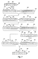
- Fig. 7 is a flow diagram illustrating two implementations of the general acts described in relation to Fig. 4 that employ extra bits, called buffer bits, between component data items.
- the first implementation illustrated by operands 200 through 250, performs an addition operation
- the second illustrated by operands 250 through 300, performs a subtraction operation.
- Composite operand 200 includes a plurality of component data items. As shown, components 202 and 204 are adjacent to each other within operand 200.
- a spread operation can be performed on operand 200 to obtain composite operand 210.
- Operand 210 includes component 212 with the same value as component 202 and component 214 with the same value as component 204.
- operand 210 includes buffer bit 216 between components 212 and 214.
- any spread operation can be used that uses a composite operand to obtain another composite operand that includes one or more buffer bits between adjacent component data items.
- a spread operation could be implemented using spreading circuitry.
- the number of buffer bits could be large enough to ensure that the resulting data item produced in each component's subarray would not affect an adjacent subarray, but this may be inefficient.
- the number of buffer bits should preferably be kept at a minimum.
- each component data item includes ((M/n) -1) bits or less, where n is an integer
- n components can be included in one M-bit composite operand if one buffer bit can be inserted at or adjacent the least significant bit or at or adjacent the most significant bit of every component data item. In these cases, all arithmetic can be done MOD 2 n - 1 .
- buffer bits are inserted by spreading components, range and resolution of component values are preserved but additional processing positions are used for buffer bits. If buffer bits replace least significant bits of components, precision or resolution of component values is sacrificed. If buffer bits replace most significant bits, the range of component values is reduced by half.
- a buffer bit at or adjacent the most significant bit may conveniently be used to indicate a binary result of an arithmetic operation for a pixel, as described in the copending, concurrently filed European Patent Application EP-A-0 602 887.
- each component data item includes more than ((M/n) -1) but not more than (M/n) bits, and if some precision can be sacrificed, then n component data items can be included in one M-bit composite operand if the least significant bits of some or all components are used as buffer bits. In this case, arithmetic operations are performed on even numbers only.
- operand 210 is ANDed with operand 220, a mask operand that is ON in every bit position in a component's subarray and is OFF in every buffer bit position, as shown by bit 222.
- the AND operation produces composite operand 230, with component 232 having the same value as component 212 and with component 234 having the same value as component 214.
- Buffer bit 236 has the value zero.
- the addition operation adds composite operand 230 to composite operand 240, the relevant part of which is illustratively shown as identical to operand 230, with components 242 and 244 the same as components 232 and 234 and with buffer bit 246 the same as buffer bit 236.
- Operand 240 could be obtained by copying operand 230 or could be obtained by acts similar to those described above. If a constant was being added to each component in a composite operand, the constant operand could be obtained starting with an all-zero operand with which the constant could be ORed at the position of each component's subarray.
- Addition of operands 230 and 240 produces composite operand 250, with a resulting data item in each component's subarray Resulting data item 252 indicates a valid result of adding components 232 and 242, while resulting data item 254 indicates a valid result of adding components 234 and 244.
- Buffer bit 256 has the value one because of carry signal 258 received from the subarray in which components 234 and 244 are added, but buffer bit 256 has ensured that resulting data items 252 and 254 indicate valid results. If another addition were performed, buffer bit 256 would be cleared again before adding.
- Operands 200 through 250 thus illustrate an implementation of the acts in Fig. 4.
- Operands 200, 210, 230, and 240 illustrate how each component data item is provided to a subarray.
- Operands 230, 240, and 250 illustrate how an arithmetic operation is performed in parallel to obtain valid results despite an inter-component signal, carry signal 258.
- a two's complement subtraction operation can be implemented by inverting a subtrahend and adding to it a minuend plus a carry to produce a difference between the minuend and the subtrahend. Therefore, to obtain a valid result for each component, it is necessary to add a carry into each resulting data item. This can be done using buffer bits, provided that the buffer bits in both the minuend operand and the inverted subtrahend operand have the value one, so that they are certain to produce a carry signal to the next subarray.
- composite operand 250 is the minuend operand, but it may have zeros in some buffer bits. Therefore, to prepare it for a subtraction operation, it is ORed with operand 260, a mask operand that is OFF in every bit position in a component's subarray and is ON in every buffer bit position, as shown by bits 262 and 264.
- Mask 260 can be seen to be the complement of mask 220. An implementation can store one of the two masks, inverting as required to obtain the other.
- the OR operation produces composite operand 270, with component 272 having the same value as component 252 and with component 274 having the same value as component 254.
- Buffer bits 276 and 278 have the value one.
- Composite operand 280 is the subtrahend, illustratively obtained by ORing a constant 11 with each subarray in an all-zero operand, so that constant data items 282 and 284 each have the value 11 and buffer bits 286 and 288 each have the value zero. The subtrahend must be obtained such that all buffer bits have the value zero. Then, operand 280 is inverted to obtain operand 290, in which constant data items 292 and 294 each have the value 00 and buffer bits 296 and 298 each have the value one. The inversion operation is conventionally performed by an arithmetic logic unit (ALU) as part of a two's complement subtraction operation so it need not be implemented in code.
- ALU arithmetic logic unit
- An addition operation then adds operand 270 to operand 290 to obtain operand 300, with a resulting data item in each subarray.
- Resulting data item 302 indicates a valid result of subtracting constant data item 282 from component 252 because of carry signal 304, while resulting data item 306 indicates a valid result of subtracting constant data item 284 from component 254 because of carry signal 308.
- Operands 250 through 300 thus illustrate an implementation of the acts in Fig. 4.
- Operands 250, 270, 280, and 290 illustrate how each component data item is provided to a subarray.
- Operands 270, 290, and 300 illustrate how an arithmetic operation is performed in parallel to obtain valid results despite inter-component signals, carry signals 304 and 308.
- multiplication and division operations can also be performed using buffer bits together with techniques that produce masks.
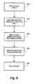
- Fig. 8 illustrates another implementation of the general acts described in relation to Fig. 4 that biases values of component data items. This implementation depends on constraints applied to values of composite operands.
- the act in box 350 receives input values. These values are constrained to positive numbers with no more than q bits, so that they can range from 0 to 2 q .
- the act in box 352 forms a composite operand with a subarray for each input value. All subarrays can be of the same length, which must exceed log 2 ( n + m).
- the act in box 354 biases the components by adding n to the value in each subarray, ensuring a non-negative result when a stored value is added to the subarray.
- the act in box 356 then adds a stored value to each subarray, obtaining values that can range from zero to (n + m ).
- the stored values added by the act in box 356 must be adjusted to ensure that carry signals do not lead to invalid results.
- the adjustment can be done by scanning the stored values to be added to the composite operand leftward from the least significant end to the most significant end. If a stored value is less than zero, as indicated by a one in its most significant bit, one is subtracted from the next stored value to the left. This procedure is effective because each negative stored value would produce a carry signal while none of the non-negative stored values would. As a result of this adjustment, the carry signals produced by adding negative stored values lead to valid results.
- the act in box 358 then adjusts the results from box 356.
- the act in box 358 could, for example, subtract n from each subarray, reversing the act in box 354.
- each subarray would include a valid result of adding an input value received in box 350 to a stored value prior to the adjustment referred to in box 356.
- the subtraction in box 358 could be done in more than one way. One way would be to handle each subarray separately; the value in each subarray could be used to access a lookup table to obtain another value reduced by n from the value in the subarray. Another way would be to provide a lookup table for the result from box 356. Other adjustments could be made as desired, to truncate or otherwise obtain data suitable for subsequent operations.
- Fig. 8 The implementation of Fig. 8 would be useful for adding entries from a table, as in dithering pixel values. It could be extended for use in other situations.
- the general implementation features described above could be used in a wide variety of data processing applications. They are expected to be particularly useful, however, in performing some types of image processing more rapidly than they could be performed serially on each component data item.
- the features described above could be used to implement techniques similar to those described in Serra, J., Image Analysis and Mathematical Morphology, Academic Press, 1982 and Serra, J., Image Analysis and Mathematical Morphology, Volume 2: Theoretical Advances, Academic Press, 1988.
- Such techniques may be used, for example, to provide document services, such as removal of noise or other non-informative features, skew correction, data encoding, extraction of segments for automatic form or control sheet creation, and printer specific correction.
- Such document services can be used in digital copying machines, including fax machines and photocopying machines, in machines that produce data defining an image for a printer or other image output device, in machines that operate on data defining an image received from a scanner or other image input device, and in other machines that perform image processing.
- the general implementation features described above may also be useful in various other applications, such as searching an image database for images containing a particular set of features; scanning envelopes for addresses; interpreting forms from a high-speed scanner; machine vision; and process-specific print image correction and verification.
- the invention could also be applied to perform various other image processing operations, such as pixel counting, gray scale morphology, gray scale rotation, generating error-diffused images, and skew detection.
- the invention could also be used with data that does not relate to an image.
- the invention could be used, for example, to perform finite difference analysis or simulations of physical phenomena.
- the invention has been described in relation to implementations in which component data items in an composite operand are separated by single buffer bits.
- the invention could also be implemented with plural buffer bits between component data items.
- inter-component prevent circuitry that includes gating circuitry or a mask register
- the invention might also be implemented with other types of inter-component prevent circuitry. If used with a processor that provides carry look-ahead signals or other such signals, the inter-component prevent circuitry could also prevent such signals from causing invalid results.
- the invention has been described in relation to implementations that operate on data relating to images, but might also be implemented to operate on data that does not relate to an image.
- the invention has been described in relation to implementations that include readily available discrete components.
- the invention mignt also be implemented with custom VLSI components, and similarly with custom memory components.
- the invention has been described in relation to implementations with conventional microprocessors, but the invention might also be implemented with reduced instruction set (RISC) chips or with any other processor, including the processor of a mainframe computer, minicomputer, supercomputer, or any other computing device.
- RISC reduced instruction set
- a composite operand could include component data items of different widths, provided that other operands are aligned with components of the same widths in the same positions.
- the component data items could be arranged in groups of two or more, with the components in each group being related: If the components in each group relate to the same pixel, each component could hold a value for a respective threshold reduction. More generally, if the components in each group relate to the same location in a physical simulation space, one component could hold a value for the location and the other locations could hold derivatives at the location.
Description
- The present invention relates to techniques for performing arithmetic operations on data.
- Wilson, US-A 5,129,092 ("Wilson '092"), describes techniques for processing data matrices such as images and spatially related data using neighborhood processing units. As shown and described in relation to Figs. 1 and 2, the processing units form an array with several groups of eight processing units. Each processing unit's connections to its adjacent processing units to the immediate left and right in the array include a carry in line to its left and a carry out line to the right.
- Wilson '092 describes arithmetic operations beginning at col. 12
line 40. In bit serial arithmetic, a carry signal from a carry flip-flop is passed to multiplexers, one of which acts as a truth table for a carry propagate value, which is stored in flip-flops, provided to an output selector, and can be read back to memory. In parallel arithmetic, a carry input from a processing unit to the immediate left is obtained and a carry output propagates to a processing unit to the immediate right. When performing parallel arithmetic operations, care must be used in writing algorithms in order to avoid overflow, so that carry signals will not accidentally propagate from one data word to the next, since many data words are on the same line of bits. - Mahoney, EP-A 460 970, describes techniques for operating on a body of data such as data defining an image. Fig. 7 shows a Connection Machine system that performs image processing by simulating a binary image jungle (BIJ). A front end processor can make calls to cause processing units in the Connection Machine to perform arithmetic and logical operations. Fig. 8 illustrates a part of an array of processing units in a Connection Machine, with a processing unit storing a pixel value of an image at a lowest level of a BIJ and receiving a pixel value from another processing unit at the next higher level of the BIJ. As described at
page 20 lines 15-28 in relation to Fig. 10, each processing unit operates on the results from the next lower level of its first and second children. Figs. 13 and 14 each show a sequence of data item arrays in which sums of pixel values are obtained. As described in relation to Fig. 18, each processing unit's local memory can contain a respective pixel's value. - EP-A-0 464 601 discloses an arithmetic operation system in which a carry control indication register stores carry control information for each of a plurality of cascaded arithmetic units. Each arithmetic unit includes a carry controller that receives a carry control bit from the carry control indication register and, based on the carry control bit, modifies an output carry from the arithmetic unit before it is supplied to the adjacent more significant bit arithmetic unit. The system can be partitioned into fields at arbitrary positions.
- EP-A-0 486 143 discloses techniques for parallel processing of data in which, before processing, operands are packed into a word with at least one cleared buffer bit between each operand. The buffer bit is cleared before any arithmetic or logical operation involving signed arithmetic and again before evaluating results. This prevents propagation of a signed bit from flowing into bits of another operand's result.
- It is the object of the present invention to provide a method of operating a processor to perform arithmetic operations with high processing speed.
- This object is solved by subject matter of
claim 1. - Preferred embodiments of the present invention are the subject matter of the dependent claims.
- Some operations, referred to herein as "logic operations," obtain one result bit using each operand bit. Therefore, a logic operation produces valid results when performed in parallel on a composite operand that includes a plurality of component data items. Examples include NOT, AND, OR, and XOR.
- In contrast, ordinary arithmetic operations can obtain a result with more bits than the values on which the operations are performed. For example, adding two K-bit values can produce a (K + 1)-bit result because of a carry signal. Subtracting one K-bit value from another that is smaller can result in a borrow signal to the (K + 1)th bit. Multiplying two K-bit values can produce a 2K-bit result. And division can sometimes produce an unlimited number of bits if not truncated at some level of precision.
- Because results of greater widtn could be produced, conventional processors cannot perform ordinary arithmetic operations in parallel on composite operands that include plural component data items such as pixel values. An operation on one component may produce an inter-component signal, such as a carry signal, a borrow signal, or a shift, that propagates or overflows into the next component, invalidating the result obtained from the next component. If the components are bits, logic operations can be used rather than arithmetic operations to solve this problem. But if the components contain more than one bit, logic operations cannot satisfactorily replace arithmetic operations.
- The invention strives to provide improved techniques that perform arithmetic operations in parallel on composite operands that include plural multi-bit component data items. For example, each component could relate to a pixel of an image; the components can be gray scale or color pixel values.
- Although the arithmetic operations would ordinarily produce signals between components, referred to herein as "inter-component signals," that would cause invalid results, the techniques of the invention produce valid results. Some techniques use a processor with special circuitry that can prevent inter-component signals. Others, which can use a conventional processor, obtain valid results of an arithmetic operations despite inter-component signals.
- Each technique that can use a conventional processor can be implemented in an article of manufacture The article includes a data storage medium and instruction data stored by the data storage medium, which could be a magnetic storage medium, an optical storage medium, a semiconductor memory, or other memory medium. The article can be used in a system that includes memory, a storage medium access device, and a processor. The memory stores multi-bit data items, such as data relating to pixels of an image. The instruction data indicate instructions a processor can execute to perform an arithmetic operation in parallel on a composite operand that includes more than one of the multi-bit data items. The instructions ensure that the results obtained are valid despite inter-component signals. The instruction data can be, for example, code that can be executed by a microprocessor such as the CPU of a conventional workstation or other computer.
- One special circuitry technique uses a processor with gating circuitry that can be used to control transfer of signals between component data items. This technique can use conventional microprocessors if the maximum component width is an integer multiple of the microprocessor width.
- Another special circuitry technique uses a processor with a mask register connected to the processing circuitry. The mask register could be loaded with an allow value, such as ON, in bit positions that are allowed to receive inter-component signals from the next lower bit positions. The mask register could be loaded with a prevent value, such as OFF, in bit positions that are not allowed to receive inter-component signals from the next lower bit positions. The mask register could be loaded each time component width changes, allowing many component widths. Also, for operations on data other than composite operands, the mask register can be loaded with values that permit inter-component signals to propagate freely.
- One technique that can use a conventional processor uses one or more buffer bits between each pair of adjacent component data items. For example, a buffer bit could be annexed to every component, above its most significant bit or below its least significant bit. Or, if precision can be sacrificed, the least significant bit of each component could be a buffer bit. The values of the buffer bits can then be manipulated to prevent or compensate for inter-component signals.
- An addition operation can clear all buffer bits before adding composite operands. For example, if the operation adds pairs of components, each composite operand can be ANDed with a mask having an OFF value in each buffer bit and an ON value elsewhere. If the operation adds a constant to every component, a constant operand can be formed by replicating the constant separated by buffer bits that have an OFF value.
- A subtraction operation can use a buffer bit above each component's most significant bit. To ensure valid results, each buffer bit in a composite minuend can have ON values and each buffer bit in a composite subtrahend can start with an OFF value. In effect, the buffer bits ensure that each component of the minuend has a value exceeding the aligned component of the subtrahend. As a result, a borrow signal cannot propagate to the next component's result.
- Multiplication and division can be implemented with addition and subtraction, together with shifting and logic operations using masks. The buffer bits can be used to generate the masks.
- The buffer bit technique can also be implemented using special circuitry that inserts buffer bits between component data items.
- Another technique that can use a conventional processor can be used to reduce or eliminate buffer bits for certain arithmetic operations. This technique prepares composite operands for an addition operation by adjusting values indicated by component data items. For example, if it can be predicted that a certain component's value will cause an inter-component carry signal, the component adjacent its most significant bit can be adjusted by subtracting one from it prior to the operation, so that the inter-component carry signal has no effect.
- The techniques of the invention are advantageous because they provide a range of alternatives, each of which is useful in appropriate situations. Each technique can ensure that inter-component signals do not invalidate results of an arithmetic operation performed in parallel on composite operands with plural multi-bit component data items such as pixel values. In addition, some of the techniques can be used together in certain situations. As a result of the invention, arithmetic operations on multi-bit component data items can be performed rapidly and efficiently in many situations.
- The present invention will be described further, by way of example, with reference to the accompanying drawings, in which:-
- Fig. 1 is a schematic diagram showing how a valid result of an arithmetic operation on each component of a composite operand can be obtained even though the operation would ordinarily produce an inter-component signal causing an invalid result;
- Fig. 2 is a schematic block diagram showing components of a system in which a processor can execute instructions from a software product to obtain valid results of an arithmetic operation despite inter-component signals;
- Fig. 3 is a schematic block diagram showing a processor that includes inter-component prevent circuitry that can prevent inter-component signals;
- Fig. 4 is a flow chart showing acts by which a processor can obtain valid results despite inter-component signals;
- Fig. 5 is a schematic circuit diagram showing gating circuitry implementing the inter-component prevent circuitry of Fig. 3;
- Fig. 6 is a schematic circuit diagram showing mask register circuitry implementing the inter-component prevent circuitry of Fig. 3;
- Fig. 7 is a schematic flow diagram showing an addition operation and a subtraction operation, each implementing the acts in Fig. 4; and
- Fig. 8 is a flow chart showing a biasing approach that implements the acts in Fig. 4.
-
- The term "composite operand" used below is an operand that includes two or more data items, referred to as "component data items" or "components."
- A processor or other circuitry performing an arithmetic operation on a composite operand may produce an "inter-component signal." An inter-component signal is a signal like a carry signal, a borrow signal, or a shifted bit that may cause an operation on one component to affect results obtained for another component.
- An arithmetic operation "would ordinarily produce an inter-component signal from a component data item" if the operation performed according to ordinary arithmetic produces an inter-component signal whose effect extends outside the component data item. Adding one to a two-bit component data item with the value 11, for example, would ordinarily produce an inter-component carry signal affecting the next bit to the left.
- Figs. 1-4 illustrate general features of the invention. Fig. 1 shows schematically a technique that obtains a valid result of an arithmetic operation performed in parallel on multi-bit component data items. Fig. 2 shows a software product with instruction data indicating instructions a processor can perform in accordance with a technique like that in Fig. 1. Fig. 3 shows general features of a processor with inter-component prevent circuitry to prevent transfer of inter-component signals between processing positions. Fig. 4 shows general acts in a method of operating a processor to obtain valid results despite an inter-component signal.
- In Fig. 1,
composite operand 10 includescomponent data items Component 12 has thevalue 01, whilecomponent 14 has thevalue 10. Similarly,composite operand 20 includescomponents respective values -
Components components components components operation adding operand 10 tooperand 20,components components - An ordinary arithmetic operation of addition performed on
composite operands result 30. As shown, result 30 includesdata items values 11 and 00 respectively. The "1" values indata item 32 both result from carry signals, carrysignal 36 from the most significant bit ofcomponents signal 38 from the least significant bit ofcomponents signal 36 causes an invalid result indata item 32, because the sum of 01 and 01 is 10, not 11. - In order to avoid
invalid result 30, the processor can instead producevalid result 40, in whichdata items values - Fig. 2 shows
software product 60, an article of manufacture that can be used in a system that includes components like those shown in Fig. 2.Software product 60 includesdata storage medium 62 that can be accessed by storagemedium access device 64.Data storage medium 62 could, for example, be a magnetic medium such as a set of one or more floppy disks, an optical medium such as a set of one or more CD-ROMs, semiconductor memory, or any other appropriate medium for storing data. -
Data storage medium 62 stores data that storagemedium access device 64 can provide to processor 66, which could for example be a microprocessor. Processor 66 is connected for receiving data frominput circuitry 70. The data could be obtained from any appropriate source, such as a facsimile (fax) machine; a scanner, which could be the scanner of a digital copier or an input/output device of a computer; an editor, which could be a forms editor or other interactive image editor controlled by user input devices such as a keyboard and mouse or a pen- or stylus-based input device; or a network, which could be a local area network or other network capable of transmitting data. The data could relate to an image. - Processor 66 is also connected for providing data to
output circuitry 80. The data could in turn be provided to a fax machine, a printer, a display, or a network. The printer could be the printer of a digital copier or an input/output device of a computer. - In addition to
data storage medium 62,software product 60 includes data stored bystorage medium 62. The stored data include instruction data indicatingarithmetic operation instructions 90. Processor 66 can executeinstructions 90 to perform an arithmetic operation on a composite operand that includes a plurality of component data items. - Processor 66 can obtain the component data items on which the arithmetic operation is performed by accessing
memory 92. Each item of data can, for example, relate to a pixel of an image. The items of data can each include more than one bit. The data stored bystorage medium 62 could also include data indicating instructions processor 66 can execute to store data items received frominput circuitry 70 inmemory 92, to retrieve data items frommemory 92 for an arithmetic operation or to be provided tooutput circuitry 80, or to store data items resulting from an arithmetic operation inmemory 92. - Processor 66 includes
processing circuitry 94 with plural processing positions 96. Processor 66 could, for example, be a conventional microprocessor. Each ofprocessing positions 96 can perform an operation on one bit.Processing circuitry 94 includesposition connecting circuitry 98 connectingprocessing positions 96 in pairs to form an array. A signal from one processing position in a pair can be transferred byposition connecting circuitry 98 to the other processing unit. - Each component data item in a composite operand on which an arithmetic operation is being performed can be in a respective subarray of processing positions 96. Processor 66 can execute
arithmetic operation instructions 90 to obtain a resulting data item in each component's subarray. During execution ofarithmetic operation instructions 90, the subarray of a first component provides an inter-component signal to position connectingcircuitry 98. The inter-component signal is capable of causing the arithmetic operation to obtain a resulting data item indicating an invalid result in the subarray of a second component. Processor 66, in executingarithmetic operation instructions 90, acts to ensure that the resulting data item in the second component's subarray indicates a valid result of the arithmetic operation on the second component, despite the inter-component signal. - Fig. 3 shows general components of a
processor 100.Processing circuitry 102 can perform arithmetic operations in parallel on composite operands. Like processingcircuitry 94 in Fig. 2,processing circuitry 102 has plural processing positions 104. Each ofprocessing positions 104 can perform an operation on one bit.Processing circuitry 102 includesposition connecting circuitry 106 connectingprocessing positions 104 in pairs to form an array. A signal from one processing position in a pair can be transferred byposition connecting circuitry 106 to the other processing unit. -
Processor 100 is not, however, a conventional microprocesor. Inter-component preventcircuitry 110 is connected so that it can prevent transfer of signals betweenprocessing positions 104 throughposition connecting circuitry 106. -
Control circuitry 112 is connected to provide control signals toprocessing circuitry 102 and inter-component preventcircuitry 110. - The control signals cause
processing circuitry 102 to perform an arithmetic operation in parallel on a composite operand that includes plural multi-bit component data items. For example, each component data item can relate to a pixel of an image. Each component is in a respective subarray of processing positions 104.Processing circuitry 102 performs the arithmetic operation on each component to obtain a resulting data item in each component's subarray. During performance of the arithmetic operation, the subarray of a first component provides an inter-component signal to position connectingcircuitry 106. The inter-component signal is capable of causing the arithmetic operation to obtain a resulting data item indicating an invalid result in the subarray of a second component. - The control signals also cause inter-component prevent
circuitry 110 to prevent transfer of the inter-component signal byposition connecting circuitry 106. As a result, the resulting data item in the second component's subarray indicates a valid result of the arithmetic operation on the second component. - Fig. 4 shows general acts in a method of operating a processor with processing circuitry like processing
circuitry 94 in Fig. 2. The act inbox 130 provides a composite operand to processingcircuitry 94, with each component being provided to a respective subarray of processing positions 96. The act inbox 132 operatesprocessing circuitry 94 to perform an arithmetic operation in parallel on the composite operand to obtain a resulting data item in each subarray. During performance of the arithmetic operation, the subarray of a first component provides an inter-component signal. The act inbox 132 is performed so as to ensure that each resulting data item indicates a valid result despite the inter-component signal. - The general features described above in relation to Figs. 1-4 could be implemented in many different ways with a wide variety of components and with various operations. For example, some of the general features described above have been implemented with conventional processors while others could be implemented with specially designed processors.
- Figs. 5 and 6 illustrate two implementations of the general components shown in Fig. 3. Figs. 7 and 8 illustrate two implementations of the general steps shown in Fig. 4 that are applicable for processing units that can operate in parallel on more than one data item; a number of such processing units could be used in parallel without position connecting circuitry between them.
- Fig. 5 illustrates an implementation of the general components described in relation to Fig. 3 that can employ conventional microprocessors in
processing circuitry 102. The implementation in Fig. 5 includes inter-component preventcircuitry 110 that can prevent an inter-component signal between the microprocessors. Therefore, if each microprocessor is M bits wide, where M ≥ 1, the array of processing positions can be divided into subarrays at any integer multiple of M bits. Each subarray can then perform arithmetic operations on component data items. - Fig. 5 shows
microprocessor 150, the pth microprocessor in an array of microprocessors that provides processing positions 104. Within the array,position connecting circuitry 106 connects the carry in and carry out leads of adjacent microprocessors. As shown, however, the carry in lead ofmicroprocessor 150 receives a signal from the carry out lead of the (p - 1)th microprocessor only if a carry select signal is provided to ANDgate 152. Similarly, a signal from the carry out lead ofmicroprocessor 150 is provided to the (p + 1)th microprocessor only if a carry select signal is provided to ANDgate 154. - Width-to-
select decoder 156 can be a read only memory (ROM), programmable array logic (PAL), or other conventional circuitry that responds to a signal fromcontrol circuitry 112 by providing carry enable signals to the appropriate AND gates so that carry signals can be transferred within a subarray but not between subarrays of different component data items. The signal fromcontrol circuitry 112 can indicate a subarray width, such as M, 2M, 3M, and so forth, and the output from width-to-select decoder 156 can accordingly be ON for AND gates within a subarray and OFF for AND gates between subarrays. To perform an operation on an array-wide value, which is useful for tasks that tend to generate large numbers such as pixel counting, the signal fromcontrol circuitry 112 can indicate a width such that the output from width-to-select decoder 156 provides an ON output to all AND gates. - Fig. 6 illustrates another implementation of the general components described in relation to Fig. 3 that can employ a customized arithmetic logic unit (ALU) 170. The implementation in Fig. 6 includes inter-component prevent circuitry that can prevent an inter-component signal between any two adjacent processing positions within
ALU 170. Therefore, ifALU 170 is M bits wide, the array of processing positions can be divided into equal subarrays at any integer factor of M bits. Each subarray can then perform arithmetic operations on component data items. -
Processing position 172 is the pth position inprocessing positions 104 withinALU 170. Within the array, position connecting circuitry as in Fig. 3 connects carry in and carry out leads of adjacent processing positions. As shown, however, the carry in lead ofposition 172 receives a signal from the carry out lead of the (p - 1)th position throughposition connecting logic 174. Similarly, the carry out lead ofposition 172 provides a signal to the carry in lead of the (p + 1)th position throughposition connecting logic 176. -
Position connecting logic 174 provides a carry in signal from the (p - 1)th position only if an ON value is provided to the other input lead of ANDgate 180, so that the signal is provided to the carry in lead ofposition 172 through ORgate 182. When the mask register provides an OFF signal to ANDgates position 172 receives an ON signal only if the subtract signal to ANDgate 184 is ON.Position connecting logic 176 includes similar circuitry. -
Mask register 190 can be implemented with conventional register circuitry that can be loaded with mask values by signals fromcontrol circuitry 112. The mask values include enable values, illustratively ON, and prevent values, illustratively OFF.Mask register 190 is connected so that each mask value is provided to AND gates that control the carry in line of a respective position like ANDgates Mask value 192 controls the carry in line of the (p - 1)th position,mask value 194 the carry in line of the pth position, andmask value 196 the carry in line of the (p + 1)th position. In general, an enable value allows a carry out signal from the next lower position to propagate upward, while a prevent value prevents upward propagation of carry out signals. But during a subtraction operation, a prevent value provides a carry in signal even if the next lower position is not providing a carry out signal, as required by the standard implementation of two's complement arithmetic. -
Control circuitry 112 can loadmask register 190 each time the number of bits in each component data item changes. For instance, if the component data items are pixel values, mask values can be changed whenever the number of bits in each pixel value changes. - In the illustrated example,
mask value 192 controls the uppermost processing position of one component's subarray, whilemask value 194 controls the lowermost processing position of an adjacent component's subarray, which isposition 172. - Each of the above implementations employs special circuitry. In contrast, the following implementations do not require special circuitry, but may use processing positions less efficiently than the above implementations due to additional bits such as buffer bits.
- Fig. 7 is a flow diagram illustrating two implementations of the general acts described in relation to Fig. 4 that employ extra bits, called buffer bits, between component data items. The first implementation, illustrated by
operands 200 through 250, performs an addition operation, the second, illustrated byoperands 250 through 300, performs a subtraction operation. -
Composite operand 200 includes a plurality of component data items. As shown,components operand 200. - A spread operation can be performed on
operand 200 to obtaincomposite operand 210.Operand 210 includescomponent 212 with the same value ascomponent 202 andcomponent 214 with the same value ascomponent 204. In addition,operand 210 includesbuffer bit 216 betweencomponents - In general, any spread operation can be used that uses a composite operand to obtain another composite operand that includes one or more buffer bits between adjacent component data items. For example, a spread operation could be implemented using spreading circuitry. The number of buffer bits could be large enough to ensure that the resulting data item produced in each component's subarray would not affect an adjacent subarray, but this may be inefficient.
- For maximum efficiency, the number of buffer bits should preferably be kept at a minimum.
- If an M-bit microprocessor is being used, for example, and each component data item includes ((M/n) -1) bits or less, where n is an integer, then n components can be included in one M-bit composite operand if one buffer bit can be inserted at or adjacent the least significant bit or at or adjacent the most significant bit of every component data item. In these cases, all arithmetic can be done MOD 2n - 1.
- If buffer bits are inserted by spreading components, range and resolution of component values are preserved but additional processing positions are used for buffer bits. If buffer bits replace least significant bits of components, precision or resolution of component values is sacrificed. If buffer bits replace most significant bits, the range of component values is reduced by half.
- In addition, a buffer bit at or adjacent the most significant bit may conveniently be used to indicate a binary result of an arithmetic operation for a pixel, as described in the copending, concurrently filed European Patent Application EP-A-0 602 887.
- If each component data item includes more than ((M/n) -1) but not more than (M/n) bits, and if some precision can be sacrificed, then n component data items can be included in one M-bit composite operand if the least significant bits of some or all components are used as buffer bits. In this case, arithmetic operations are performed on even numbers only.
- Before an addition operation that adds aligned components in two composite operands, each buffer bit in both operands should be cleared to zero to prevent propagation of carry signals from one component's subarray to another's. Therefore,
operand 210 is ANDed withoperand 220, a mask operand that is ON in every bit position in a component's subarray and is OFF in every buffer bit position, as shown bybit 222. - The AND operation produces
composite operand 230, withcomponent 232 having the same value ascomponent 212 and withcomponent 234 having the same value ascomponent 214.Buffer bit 236 has the value zero. - The addition operation adds
composite operand 230 tocomposite operand 240, the relevant part of which is illustratively shown as identical tooperand 230, withcomponents components buffer bit 246 the same asbuffer bit 236.Operand 240 could be obtained by copyingoperand 230 or could be obtained by acts similar to those described above. If a constant was being added to each component in a composite operand, the constant operand could be obtained starting with an all-zero operand with which the constant could be ORed at the position of each component's subarray. - Addition of
operands composite operand 250, with a resulting data item in each component's subarrayResulting data item 252 indicates a valid result of addingcomponents data item 254 indicates a valid result of addingcomponents Buffer bit 256 has the value one because of carry signal 258 received from the subarray in whichcomponents buffer bit 256 has ensured that resultingdata items buffer bit 256 would be cleared again before adding. -
Operands 200 through 250 thus illustrate an implementation of the acts in Fig. 4.Operands Operands - A two's complement subtraction operation can be implemented by inverting a subtrahend and adding to it a minuend plus a carry to produce a difference between the minuend and the subtrahend. Therefore, to obtain a valid result for each component, it is necessary to add a carry into each resulting data item. This can be done using buffer bits, provided that the buffer bits in both the minuend operand and the inverted subtrahend operand have the value one, so that they are certain to produce a carry signal to the next subarray.
- In Fig. 7,
composite operand 250 is the minuend operand, but it may have zeros in some buffer bits. Therefore, to prepare it for a subtraction operation, it is ORed withoperand 260, a mask operand that is OFF in every bit position in a component's subarray and is ON in every buffer bit position, as shown bybits Mask 260 can be seen to be the complement ofmask 220. An implementation can store one of the two masks, inverting as required to obtain the other. - The OR operation produces
composite operand 270, withcomponent 272 having the same value ascomponent 252 and withcomponent 274 having the same value ascomponent 254.Buffer bits -
Composite operand 280 is the subtrahend, illustratively obtained by ORing a constant 11 with each subarray in an all-zero operand, so thatconstant data items buffer bits operand 280 is inverted to obtainoperand 290, in whichconstant data items value 00 andbuffer bits - An addition operation then adds
operand 270 tooperand 290 to obtainoperand 300, with a resulting data item in each subarray. Resultingdata item 302 indicates a valid result of subtractingconstant data item 282 fromcomponent 252 because ofcarry signal 304, while resultingdata item 306 indicates a valid result of subtractingconstant data item 284 fromcomponent 254 because ofcarry signal 308. -
Operands 250 through 300 thus illustrate an implementation of the acts in Fig. 4.Operands Operands signals - As described in copending, concurrently filed European Patent Application EP-A-0 602 886, multiplication and division operations can also be performed using buffer bits together with techniques that produce masks.
- Fig. 8 illustrates another implementation of the general acts described in relation to Fig. 4 that biases values of component data items. This implementation depends on constraints applied to values of composite operands.
- The act in
box 350 receives input values. These values are constrained to positive numbers with no more than q bits, so that they can range from 0 to 2 q . The implementation shown in Fig. 8 performs an arithmetic operation that adds a stored value, such as a value from a table, to each input value, and the stored values are similarly constrained to positive or negative numbers with no more than r bits, ranging between ± (2 r-1- 1). If q = r = 4, for example, input values can range from zero to 15 while stored values can range from - 7 to + 7. In this example, the arithmetic operation can obtain values ranging from - 7 to + 22. In general, an arithmetic operaion that adds a stored value to an input value can obtain values ranging from - n to + m where n and m are positive integers. - The act in
box 352 forms a composite operand with a subarray for each input value. All subarrays can be of the same length, which must exceed log2(n + m). - The act in
box 354 biases the components by adding n to the value in each subarray, ensuring a non-negative result when a stored value is added to the subarray. The act inbox 356 then adds a stored value to each subarray, obtaining values that can range from zero to (n + m). - The stored values added by the act in
box 356 must be adjusted to ensure that carry signals do not lead to invalid results. In the example set forth above, the adjustment can be done by scanning the stored values to be added to the composite operand leftward from the least significant end to the most significant end. If a stored value is less than zero, as indicated by a one in its most significant bit, one is subtracted from the next stored value to the left. This procedure is effective because each negative stored value would produce a carry signal while none of the non-negative stored values would. As a result of this adjustment, the carry signals produced by adding negative stored values lead to valid results. - The act in
box 358 then adjusts the results frombox 356. The act inbox 358 could, for example, subtract n from each subarray, reversing the act inbox 354. As a result, each subarray would include a valid result of adding an input value received inbox 350 to a stored value prior to the adjustment referred to inbox 356. The subtraction inbox 358 could be done in more than one way. One way would be to handle each subarray separately; the value in each subarray could be used to access a lookup table to obtain another value reduced by n from the value in the subarray. Another way would be to provide a lookup table for the result frombox 356. Other adjustments could be made as desired, to truncate or otherwise obtain data suitable for subsequent operations. - The implementation of Fig. 8 would be useful for adding entries from a table, as in dithering pixel values. It could be extended for use in other situations.
- The general implementation features described above could be used in a wide variety of data processing applications. They are expected to be particularly useful, however, in performing some types of image processing more rapidly than they could be performed serially on each component data item. In particular, the features described above could be used to implement techniques similar to those described in Serra, J., Image Analysis and Mathematical Morphology, Academic Press, 1982 and Serra, J., Image Analysis and Mathematical Morphology, Volume 2: Theoretical Advances, Academic Press, 1988. Such techniques may be used, for example, to provide document services, such as removal of noise or other non-informative features, skew correction, data encoding, extraction of segments for automatic form or control sheet creation, and printer specific correction. Such document services can be used in digital copying machines, including fax machines and photocopying machines, in machines that produce data defining an image for a printer or other image output device, in machines that operate on data defining an image received from a scanner or other image input device, and in other machines that perform image processing.
- The features described above can be used to perform arithmetic operations on gray scale or color pixel values during a wide variety of image processing operations.
- The general implementation features described above may also be useful in various other applications, such as searching an image database for images containing a particular set of features; scanning envelopes for addresses; interpreting forms from a high-speed scanner; machine vision; and process-specific print image correction and verification.
- The invention could also be applied to perform various other image processing operations, such as pixel counting, gray scale morphology, gray scale rotation, generating error-diffused images, and skew detection.
- The invention could also be used with data that does not relate to an image. The invention could be used, for example, to perform finite difference analysis or simulations of physical phenomena.
- The invention has been described in relation to several implementations. The invention might also be implemented by using two or more of the implementations together.
- The invention has been described in relation to implementations in which component data items in an composite operand are separated by single buffer bits. The invention could also be implemented with plural buffer bits between component data items.
- The invention has been described in relation to inter-component prevent circuitry that includes gating circuitry or a mask register The invention might also be implemented with other types of inter-component prevent circuitry. If used with a processor that provides carry look-ahead signals or other such signals, the inter-component prevent circuitry could also prevent such signals from causing invalid results.
- The invention has been described in relation to addition and subtraction, but could be applied to other arithmetic operations, including multiplication, division, and threshold convolution, as described in copending, concurrently filed European Patent Application EP-A-0 602 886.
- The invention has been described in relation to implementations that operate on data relating to images, but might also be implemented to operate on data that does not relate to an image.
- The invention has been described in relation to implementations that include readily available discrete components. The invention mignt also be implemented with custom VLSI components, and similarly with custom memory components.
- The invention has been described in relation to implementations with conventional microprocessors, but the invention might also be implemented with reduced instruction set (RISC) chips or with any other processor, including the processor of a mainframe computer, minicomputer, supercomputer, or any other computing device.
- The invention has been described in relation to composite operands with simple structures. In the examples described above, all component data items are of the same length and the components within a composite operand need not be related to each other The invention could also be implemented with composite operands with additional structure, within the limitations of processor width. For example, a composite operand could include component data items of different widths, provided that other operands are aligned with components of the same widths in the same positions. Also, the component data items could be arranged in groups of two or more, with the components in each group being related: If the components in each group relate to the same pixel, each component could hold a value for a respective threshold reduction. More generally, if the components in each group relate to the same location in a physical simulation space, one component could hold a value for the location and the other locations could hold derivatives at the location.
Claims (7)
- A method of operating a processor (66) that includes processing circuitry (94) for performing arithmetic oeprations in parallel on operands; the processing circuitry (94) having a plurality of processing positions (96), each for performing operations on one bit; the processing circuitry (94) including position connecting circuitry (98) connecting the processing positions (96) to form an array of processing positions; the position connecting circuitry (98) connecting adjacent processing positions (96) so that a signal from one of the processing positions can be transferred to an adjacent processing position;
the method including the steps of:said method being characterized in thata) providing one or more sequences (200) of two or more component data items (202, 204), each including more than one bit, to the processing positions (96) in the processing circuitry (94); each sequence having at least a first component data item (204) with a most significant bit adjacent to a least significant bit of a second component data item (202) in said sequence;b) providing a buffer bit (216, 236, 246, 256, 286, 288, 276, 278, 296, 298) between the first and second component data items in said sequence; said sequence of component data items forming a composite operand that includes the buffer bit;c) operating the processor (66) to perform an arithmetic operation in parallel on the composite operand; the arithmetic operation being an operation that would ordinarily produce an inter-component signal from the first component data item to the second component data item causing the arithmetic operation to obtain an invalid result for the second component data item; the buffer bit having a value that ensures that the arithmetic operation obtains a valid result for the second component data item despite the inter-component signal; the arithmetic operation producing, for each component data item, a respective resulting data item indicating a valid result of the arithmetic operation on the component data item;-
said buffer bit replaces either the most significant bit of the first component data item or the least significant bit of the second component data item. - A method as claimed in claim 1, in which the act of operating the processor (66) comprises obtaining a value in the position of the buffer bit so that the position of the buffer bit does not respond to the inter-component signal by providing a signal to the position connecting circuitry (98).
- A method as claimed in claim 1 or claim 2, in which the least significant bit of the second component data item is the buffer bit.
- A method as claimed in claim 1 or claim 2, in which the most significant bit of the first component data item is the buffer bit.
- A method as claimed in any preceding claim, further comprising:providing a second sequence of two or more component data items, each including more than one bit, to the processing positions (96) in the processing circuitry (94); the second sequence including a buffer bit aligned with the buffer bit in the first-mentioned sequence;the arithmetic operation being performed on the first and second sequences.
- A method as claimed in any preceding claim in which the arithmetic operation is addition and the buffer bit has the value zero.
- A method as claimed in any of claims 1 to 5 in which the arithmetic operation is subtraction and the buffer bit has the value one.
Applications Claiming Priority (2)
| Application Number | Priority Date | Filing Date | Title |
|---|---|---|---|
| US993925 | 1992-12-18 | ||
| US07/993,925 US5408670A (en) | 1992-12-18 | 1992-12-18 | Performing arithmetic in parallel on composite operands with packed multi-bit components |
Publications (2)
| Publication Number | Publication Date |
|---|---|
| EP0602888A1 EP0602888A1 (en) | 1994-06-22 |
| EP0602888B1 true EP0602888B1 (en) | 1999-09-08 |
Family
ID=25540077
Family Applications (1)
| Application Number | Title | Priority Date | Filing Date |
|---|---|---|---|
| EP93309863A Expired - Lifetime EP0602888B1 (en) | 1992-12-18 | 1993-12-08 | Performing arithmetic operations on data |
Country Status (4)
| Country | Link |
|---|---|
| US (1) | US5408670A (en) |
| EP (1) | EP0602888B1 (en) |
| JP (1) | JPH06222908A (en) |
| DE (1) | DE69326314T2 (en) |
Cited By (1)
| Publication number | Priority date | Publication date | Assignee | Title |
|---|---|---|---|---|
| KR102072543B1 (en) | 2013-01-28 | 2020-02-03 | 삼성전자 주식회사 | Multiple data type supporting adder and method for supporting adding operation of multiple data type using the adder |
Families Citing this family (60)
| Publication number | Priority date | Publication date | Assignee | Title |
|---|---|---|---|---|
| US5655131A (en) * | 1992-12-18 | 1997-08-05 | Xerox Corporation | SIMD architecture for connection to host processor's bus |
| US5651121A (en) * | 1992-12-18 | 1997-07-22 | Xerox Corporation | Using mask operand obtained from composite operand to perform logic operation in parallel with composite operand |
| US6112219A (en) * | 1993-09-23 | 2000-08-29 | Realnetworks, Inc. | Method and apparatus for performing fast discrete cosine transforms and fast inverse discrete cosine transforms using look-up tables |
| NL9400607A (en) * | 1994-04-15 | 1995-11-01 | Arcobel Graphics Bv | Data processing circuit, pipeline multiplier, ALU, and shift register unit for use with a data processing circuit. |
| ZA9510127B (en) * | 1994-12-01 | 1996-06-06 | Intel Corp | Novel processor having shift operations |
| US6738793B2 (en) | 1994-12-01 | 2004-05-18 | Intel Corporation | Processor capable of executing packed shift operations |
| US6275834B1 (en) * | 1994-12-01 | 2001-08-14 | Intel Corporation | Apparatus for performing packed shift operations |
| IL116210A0 (en) * | 1994-12-02 | 1996-01-31 | Intel Corp | Microprocessor having a compare operation and a method of comparing packed data in a processor |
| KR100329338B1 (en) | 1994-12-02 | 2002-07-18 | 피터 엔. 데트킨 | Microprocessor with packing operation of composite operands |
| GB9509989D0 (en) * | 1995-05-17 | 1995-07-12 | Sgs Thomson Microelectronics | Manipulation of data |
| US5815421A (en) * | 1995-12-18 | 1998-09-29 | Intel Corporation | Method for transposing a two-dimensional array |
| US5907842A (en) * | 1995-12-20 | 1999-05-25 | Intel Corporation | Method of sorting numbers to obtain maxima/minima values with ordering |
| US6036350A (en) * | 1995-12-20 | 2000-03-14 | Intel Corporation | Method of sorting signed numbers and solving absolute differences using packed instructions |
| US6006316A (en) * | 1996-12-20 | 1999-12-21 | International Business Machines, Corporation | Performing SIMD shift and arithmetic operation in non-SIMD architecture by operation on packed data of sub-operands and carry over-correction |
| US5946222A (en) * | 1996-12-20 | 1999-08-31 | Oak Technology, Inc. | Method and apparatus for performing a masked byte addition operation |
| US5887181A (en) * | 1997-06-23 | 1999-03-23 | Sun Microsystems, Inc. | Method and apparatus for reducing a computational result to the range boundaries of an unsigned 8-bit integer in case of overflow |
| US5901306A (en) * | 1997-06-23 | 1999-05-04 | Sun Microsystems, Inc. | Method and apparatus for reducing a computational result to the range boundaries of a signed 8-bit integer in case of overflow |
| US6041404A (en) | 1998-03-31 | 2000-03-21 | Intel Corporation | Dual function system and method for shuffling packed data elements |
| US6338135B1 (en) * | 1998-11-20 | 2002-01-08 | Arm Limited | Data processing system and method for performing an arithmetic operation on a plurality of signed data values |
| US6425003B1 (en) * | 1999-01-22 | 2002-07-23 | Cisco Technology, Inc. | Method and apparatus for DNS resolution |
| US6463521B1 (en) | 1999-06-23 | 2002-10-08 | Sun Microsystems, Inc. | Opcode numbering for meta-data encoding |
| US6363523B1 (en) * | 1999-11-12 | 2002-03-26 | Sun Microsystems, Inc. | Optimization of N-base typed arithmetic expressions |
| US8453133B2 (en) * | 1999-11-12 | 2013-05-28 | Oracle America, Inc. | Optimization of N-base typed arithmetic instructions via rework |
| US7010786B2 (en) | 1999-11-12 | 2006-03-07 | Sun Microsystems, Inc. | Predictive arithmetic overflow detection |
| US7207037B2 (en) * | 1999-11-12 | 2007-04-17 | Sun Microsystems, Inc. | Overflow sensitive arithmetic instruction optimization using chaining |
| US7107581B2 (en) * | 1999-11-12 | 2006-09-12 | Sun Microsystems, Inc. | Overflow predictive arithmetic instruction optimization using chaining |
| GB2362731B (en) | 2000-05-23 | 2004-10-06 | Advanced Risc Mach Ltd | Parallel processing of multiple data values within a data word |
| US6834337B1 (en) | 2000-09-29 | 2004-12-21 | International Business Machines Corporation | System and method for enabling multiple signed independent data elements per register |
| US7039906B1 (en) | 2000-09-29 | 2006-05-02 | International Business Machines Corporation | Compiler for enabling multiple signed independent data elements per register |
| US7155601B2 (en) * | 2001-02-14 | 2006-12-26 | Intel Corporation | Multi-element operand sub-portion shuffle instruction execution |
| US7624138B2 (en) | 2001-10-29 | 2009-11-24 | Intel Corporation | Method and apparatus for efficient integer transform |
| US7725521B2 (en) * | 2001-10-29 | 2010-05-25 | Intel Corporation | Method and apparatus for computing matrix transformations |
| US7685212B2 (en) * | 2001-10-29 | 2010-03-23 | Intel Corporation | Fast full search motion estimation with SIMD merge instruction |
| US20040054877A1 (en) | 2001-10-29 | 2004-03-18 | Macy William W. | Method and apparatus for shuffling data |
| US7739319B2 (en) * | 2001-10-29 | 2010-06-15 | Intel Corporation | Method and apparatus for parallel table lookup using SIMD instructions |
| US7631025B2 (en) * | 2001-10-29 | 2009-12-08 | Intel Corporation | Method and apparatus for rearranging data between multiple registers |
| US7818356B2 (en) | 2001-10-29 | 2010-10-19 | Intel Corporation | Bitstream buffer manipulation with a SIMD merge instruction |
| JP3779602B2 (en) * | 2001-11-28 | 2006-05-31 | 松下電器産業株式会社 | SIMD operation method and SIMD operation device |
| US7047383B2 (en) * | 2002-07-11 | 2006-05-16 | Intel Corporation | Byte swap operation for a 64 bit operand |
| GB2409062C (en) * | 2003-12-09 | 2007-12-11 | Advanced Risc Mach Ltd | Aliasing data processing registers |
| GB2409064B (en) * | 2003-12-09 | 2006-09-13 | Advanced Risc Mach Ltd | A data processing apparatus and method for performing in parallel a data processing operation on data elements |
| GB2409059B (en) * | 2003-12-09 | 2006-09-27 | Advanced Risc Mach Ltd | A data processing apparatus and method for moving data between registers and memory |
| GB2409060B (en) * | 2003-12-09 | 2006-08-09 | Advanced Risc Mach Ltd | Moving data between registers of different register data stores |
| GB2411974C (en) * | 2003-12-09 | 2009-09-23 | Advanced Risc Mach Ltd | Data shift operations |
| GB2409061B (en) * | 2003-12-09 | 2006-09-13 | Advanced Risc Mach Ltd | Table lookup operation within a data processing system |
| GB2409067B (en) * | 2003-12-09 | 2006-12-13 | Advanced Risc Mach Ltd | Endianess compensation within a SIMD data processing system |
| GB2409066B (en) * | 2003-12-09 | 2006-09-27 | Advanced Risc Mach Ltd | A data processing apparatus and method for moving data between registers and memory |
| GB2409068A (en) * | 2003-12-09 | 2005-06-15 | Advanced Risc Mach Ltd | Data element size control within parallel lanes of processing |
| GB2409065B (en) * | 2003-12-09 | 2006-10-25 | Advanced Risc Mach Ltd | Multiplexing operations in SIMD processing |
| GB2411973B (en) * | 2003-12-09 | 2006-09-27 | Advanced Risc Mach Ltd | Constant generation in SMD processing |
| GB2411976B (en) * | 2003-12-09 | 2006-07-19 | Advanced Risc Mach Ltd | A data processing apparatus and method for moving data between registers and memory |
| GB2411975B (en) * | 2003-12-09 | 2006-10-04 | Advanced Risc Mach Ltd | Data processing apparatus and method for performing arithmetic operations in SIMD data processing |
| GB2409063B (en) * | 2003-12-09 | 2006-07-12 | Advanced Risc Mach Ltd | Vector by scalar operations |
| GB2410097B (en) * | 2004-01-13 | 2006-11-01 | Advanced Risc Mach Ltd | A data processing apparatus and method for performing data processing operations on floating point data elements |
| GB2411978B (en) * | 2004-03-10 | 2007-04-04 | Advanced Risc Mach Ltd | Inserting bits within a data word |
| US9557994B2 (en) | 2004-07-13 | 2017-01-31 | Arm Limited | Data processing apparatus and method for performing N-way interleaving and de-interleaving operations where N is an odd plural number |
| US7958181B2 (en) | 2006-09-21 | 2011-06-07 | Intel Corporation | Method and apparatus for performing logical compare operations |
| US8078836B2 (en) | 2007-12-30 | 2011-12-13 | Intel Corporation | Vector shuffle instructions operating on multiple lanes each having a plurality of data elements using a common set of per-lane control bits |
| US11620169B2 (en) * | 2020-03-13 | 2023-04-04 | Nvidia Corporation | Barrierless and fenceless shared memory synchronization with write flag toggling |
| EP4235399A1 (en) * | 2022-02-28 | 2023-08-30 | Barcelona Supercomputing Center - Centro Nacional de Supercomputación (BSC-CMS) | Method for the computation of a narrow bit width linear algebra operation |
Family Cites Families (12)
| Publication number | Priority date | Publication date | Assignee | Title |
|---|---|---|---|---|
| JPS5765194A (en) * | 1980-10-09 | 1982-04-20 | Daicel Chem Ind Ltd | Microbial preparation of unsaturated dicarboxylic acid |
| US4742552A (en) * | 1983-09-27 | 1988-05-03 | The Boeing Company | Vector image processing system |
| US4608659A (en) * | 1983-09-30 | 1986-08-26 | Honeywell Information Systems Inc. | Arithmetic logic unit with outputs indicating invalid computation results caused by invalid operands |
| US4722066A (en) * | 1985-07-30 | 1988-01-26 | Rca Corporation | Digital signal overflow correction apparatus |
| US4764887A (en) * | 1985-08-02 | 1988-08-16 | Advanced Micro Devices, Inc. | Carry-bypass arithmetic logic unit |
| US5129092A (en) * | 1987-06-01 | 1992-07-07 | Applied Intelligent Systems,Inc. | Linear chain of parallel processors and method of using same |
| JP2600293B2 (en) * | 1988-06-10 | 1997-04-16 | 日本電気株式会社 | Overflow correction circuit |
| US4975868A (en) * | 1989-04-17 | 1990-12-04 | International Business Machines Corporation | Floating-point processor having pre-adjusted exponent bias for multiplication and division |
| JP2523222B2 (en) * | 1989-12-08 | 1996-08-07 | ゼロックス コーポレーション | Image reduction / enlargement method and apparatus |
| US5280547A (en) * | 1990-06-08 | 1994-01-18 | Xerox Corporation | Dense aggregative hierarhical techniques for data analysis |
| JPH0454679A (en) * | 1990-06-25 | 1992-02-21 | Nec Corp | Arithmetic unit |
| JP2601960B2 (en) * | 1990-11-15 | 1997-04-23 | インターナショナル・ビジネス・マシーンズ・コーポレイション | Data processing method and apparatus |
-
1992
- 1992-12-18 US US07/993,925 patent/US5408670A/en not_active Expired - Fee Related
-
1993
- 1993-12-08 DE DE69326314T patent/DE69326314T2/en not_active Expired - Fee Related
- 1993-12-08 EP EP93309863A patent/EP0602888B1/en not_active Expired - Lifetime
- 1993-12-17 JP JP5317778A patent/JPH06222908A/en active Pending
Cited By (1)
| Publication number | Priority date | Publication date | Assignee | Title |
|---|---|---|---|---|
| KR102072543B1 (en) | 2013-01-28 | 2020-02-03 | 삼성전자 주식회사 | Multiple data type supporting adder and method for supporting adding operation of multiple data type using the adder |
Also Published As
| Publication number | Publication date |
|---|---|
| DE69326314D1 (en) | 1999-10-14 |
| US5408670A (en) | 1995-04-18 |
| DE69326314T2 (en) | 2000-02-24 |
| EP0602888A1 (en) | 1994-06-22 |
| JPH06222908A (en) | 1994-08-12 |
Similar Documents
| Publication | Publication Date | Title |
|---|---|---|
| EP0602888B1 (en) | Performing arithmetic operations on data | |
| EP0602886B1 (en) | Masks for selecting multi-bit components in a composite operand | |
| US7389317B2 (en) | Long instruction word controlling plural independent processor operations | |
| US5680339A (en) | Method for rounding using redundant coded multiply result | |
| US6173394B1 (en) | Instruction having bit field designating status bits protected from modification corresponding to arithmetic logic unit result | |
| US5606677A (en) | Packed word pair multiply operation forming output including most significant bits of product and other bits of one input | |
| US5465224A (en) | Three input arithmetic logic unit forming the sum of a first Boolean combination of first, second and third inputs plus a second Boolean combination of first, second and third inputs | |
| US5596763A (en) | Three input arithmetic logic unit forming mixed arithmetic and boolean combinations | |
| US6098163A (en) | Three input arithmetic logic unit with shifter | |
| US5995747A (en) | Three input arithmetic logic unit capable of performing all possible three operand boolean operations with shifter and/or mask generator | |
| US5446651A (en) | Split multiply operation | |
| US5590350A (en) | Three input arithmetic logic unit with mask generator | |
| US5961635A (en) | Three input arithmetic logic unit with barrel rotator and mask generator | |
| US5485411A (en) | Three input arithmetic logic unit forming the sum of a first input anded with a first boolean combination of a second input and a third input plus a second boolean combination of the second and third inputs | |
| US6219688B1 (en) | Method, apparatus and system for sum of plural absolute differences | |
| US5640578A (en) | Arithmetic logic unit having plural independent sections and register storing resultant indicator bit from every section | |
| US6016538A (en) | Method, apparatus and system forming the sum of data in plural equal sections of a single data word | |
| US5805913A (en) | Arithmetic logic unit with conditional register source selection | |
| US6067613A (en) | Rotation register for orthogonal data transformation | |
| US5493524A (en) | Three input arithmetic logic unit employing carry propagate logic | |
| EP0602887B1 (en) | Performing arithmetic on composite operands | |
| US5596519A (en) | Iterative division apparatus, system and method employing left most one's detection and left most one's detection with exclusive OR | |
| US6026484A (en) | Data processing apparatus, system and method for if, then, else operation using write priority | |
| US5426600A (en) | Double precision division circuit and method for digital signal processor | |
| US5712999A (en) | Address generator employing selective merge of two independent addresses |
Legal Events
| Date | Code | Title | Description |
|---|---|---|---|
| PUAI | Public reference made under article 153(3) epc to a published international application that has entered the european phase |
Free format text: ORIGINAL CODE: 0009012 |
|
| AK | Designated contracting states |
Kind code of ref document: A1 Designated state(s): DE FR GB |
|
| 17P | Request for examination filed |
Effective date: 19941222 |
|
| 17Q | First examination report despatched |
Effective date: 19970401 |
|
| GRAG | Despatch of communication of intention to grant |
Free format text: ORIGINAL CODE: EPIDOS AGRA |
|
| GRAG | Despatch of communication of intention to grant |
Free format text: ORIGINAL CODE: EPIDOS AGRA |
|
| GRAH | Despatch of communication of intention to grant a patent |
Free format text: ORIGINAL CODE: EPIDOS IGRA |
|
| GRAH | Despatch of communication of intention to grant a patent |
Free format text: ORIGINAL CODE: EPIDOS IGRA |
|
| GRAA | (expected) grant |
Free format text: ORIGINAL CODE: 0009210 |
|
| AK | Designated contracting states |
Kind code of ref document: B1 Designated state(s): DE FR GB |
|
| REF | Corresponds to: |
Ref document number: 69326314 Country of ref document: DE Date of ref document: 19991014 |
|
| ET | Fr: translation filed | ||
| PLBE | No opposition filed within time limit |
Free format text: ORIGINAL CODE: 0009261 |
|
| STAA | Information on the status of an ep patent application or granted ep patent |
Free format text: STATUS: NO OPPOSITION FILED WITHIN TIME LIMIT |
|
| 26N | No opposition filed | ||
| PGFP | Annual fee paid to national office [announced via postgrant information from national office to epo] |
Ref country code: GB Payment date: 20011212 Year of fee payment: 9 Ref country code: FR Payment date: 20011212 Year of fee payment: 9 |
|
| REG | Reference to a national code |
Ref country code: GB Ref legal event code: IF02 |
|
| PGFP | Annual fee paid to national office [announced via postgrant information from national office to epo] |
Ref country code: DE Payment date: 20020109 Year of fee payment: 9 |
|
| PG25 | Lapsed in a contracting state [announced via postgrant information from national office to epo] |
Ref country code: GB Free format text: LAPSE BECAUSE OF NON-PAYMENT OF DUE FEES Effective date: 20021208 |
|
| PG25 | Lapsed in a contracting state [announced via postgrant information from national office to epo] |
Ref country code: DE Free format text: LAPSE BECAUSE OF NON-PAYMENT OF DUE FEES Effective date: 20030701 |
|
| GBPC | Gb: european patent ceased through non-payment of renewal fee | ||
| PG25 | Lapsed in a contracting state [announced via postgrant information from national office to epo] |
Ref country code: FR Free format text: LAPSE BECAUSE OF NON-PAYMENT OF DUE FEES Effective date: 20030901 |
|
| REG | Reference to a national code |
Ref country code: FR Ref legal event code: ST |