EP0602282B1 - Resequencing means for a cell switching system node - Google Patents
Resequencing means for a cell switching system node Download PDFInfo
- Publication number
- EP0602282B1 EP0602282B1 EP92203695A EP92203695A EP0602282B1 EP 0602282 B1 EP0602282 B1 EP 0602282B1 EP 92203695 A EP92203695 A EP 92203695A EP 92203695 A EP92203695 A EP 92203695A EP 0602282 B1 EP0602282 B1 EP 0602282B1
- Authority
- EP
- European Patent Office
- Prior art keywords
- cell
- memory
- tstp
- address
- output
- Prior art date
- Legal status (The legal status is an assumption and is not a legal conclusion. Google has not performed a legal analysis and makes no representation as to the accuracy of the status listed.)
- Expired - Lifetime
Links
Images


Classifications
-
- H—ELECTRICITY
- H04—ELECTRIC COMMUNICATION TECHNIQUE
- H04L—TRANSMISSION OF DIGITAL INFORMATION, e.g. TELEGRAPHIC COMMUNICATION
- H04L49/00—Packet switching elements
- H04L49/30—Peripheral units, e.g. input or output ports
- H04L49/3081—ATM peripheral units, e.g. policing, insertion or extraction
-
- H—ELECTRICITY
- H04—ELECTRIC COMMUNICATION TECHNIQUE
- H04L—TRANSMISSION OF DIGITAL INFORMATION, e.g. TELEGRAPHIC COMMUNICATION
- H04L49/00—Packet switching elements
- H04L49/30—Peripheral units, e.g. input or output ports
-
- H—ELECTRICITY
- H04—ELECTRIC COMMUNICATION TECHNIQUE
- H04Q—SELECTING
- H04Q11/00—Selecting arrangements for multiplex systems
- H04Q11/04—Selecting arrangements for multiplex systems for time-division multiplexing
- H04Q11/0428—Integrated services digital network, i.e. systems for transmission of different types of digitised signals, e.g. speech, data, telecentral, television signals
- H04Q11/0478—Provisions for broadband connections
-
- H—ELECTRICITY
- H04—ELECTRIC COMMUNICATION TECHNIQUE
- H04L—TRANSMISSION OF DIGITAL INFORMATION, e.g. TELEGRAPHIC COMMUNICATION
- H04L12/00—Data switching networks
- H04L12/54—Store-and-forward switching systems
- H04L12/56—Packet switching systems
- H04L12/5601—Transfer mode dependent, e.g. ATM
- H04L2012/5638—Services, e.g. multimedia, GOS, QOS
- H04L2012/5646—Cell characteristics, e.g. loss, delay, jitter, sequence integrity
- H04L2012/565—Sequence integrity
Definitions
- the invention relates to a resequencing device for a node of a cell switching system. It concerns more particularly switching systems in which the cells have a variable length, each cell can be consisting of a variable number of sub-cells having a length fixed.
- European patent publication No. 0 438 415 (Alcatel NV) describes a resequencing method of delaying each delay cell determined so that the total delay imposed by the switching network and by the resequencing has a substantially constant value for all cells, this value generally being chosen greater than the delay maximum that the switching network can create. If the total delay is chosen less than the maximum value of the delay that the switching network, the probability of a disturbance of the order initial is not zero, and is a function of the value chosen for the total delay. This known process has two variants.
- a first variant consists in: associating with each cell entering the switching network a time tag which indicates when the cell entered the network of switching; to extract the time label from each cell leaving the switching network; to store each cell leaving the network, until the time indicated by the label generator is equal to the time indicated in the time label of the cell, plus the total delay chosen; and then allow the emission of the cell on an output of the resequencing.
- the program is actually produced as soon as the output at which the cell and intended is available.
- the initial order of the cells is reconstructed without having to measure or estimate the transit delay of each cell across the switching network.
- the time provided by the time label generator must be available in a device located at the entrance to the network for assign time tags, and must be available simultaneously in a resequencing device located at the output of the network, to authorize the emission of each cell at a time suitable.
- this known method consists to associate with each cell leaving the network a label whose value is an estimate of the delay experienced by the cell during its transit through the network; and subject each cell to a additional delay of duration equal to the difference between the value predetermined total delay and the estimated value of the delay transit in the network, the latter being read in the label associated with each cell.
- This variant has the advantage of not not require a device associating time labels with cells arriving at the inputs of the switching network.
- the link memory provides the complete suite addresses, and therefore makes it possible to read in the buffer memory all the sub-cells of all cells with the time label considered. These cells are read in an order which is that defined by the links in the link memory, but this order has no of importance since all these cells have the same label and are addressed to the same output.
- Memory links is also used to chain in the same queue the different sequences of cell sub-cells with labels successive times, which ensures their emission in good order. This linking is achieved by matching by the memory of links the end of the sub-cell address sequence of a cell with the start of the cell sub-cell address sequence at then issue.
- This device has a first drawback which is that it does not ability to re-order cells arriving at the same entrance and being intended for several outputs, in particular when the same cell must be broadcast on several outputs.
- This impossibility follows from the operating principle of this known device, because that it needs to be stored in the address memory each time location, address start address, and address end of sequence of sub-cell addresses; and that it requires link all the sub-cells which will have to be linked subsequently be issued on the same output.
- This known device has a second drawback which is that it does not not allow the diffusion of a cell towards several exits.
- Each location of the address memory corresponds to a time unit of the generator which issues time tags. This unit of time is equal to the duration of a sub-cell.
- the time label generator did not not an infinite capacity. It therefore delivers label values identical periodically.
- Each location in the address memory is read with a constant period, at most equal to the period of time label generator. When reading a location, the constitution of the list must be completed, so that an end of list address can be validly read in the location considered. The period of the label generator therefore limit the number of sub-cells corresponding to this list, and finally limits the number of sub-cells that can have each cell.
- a first object of the invention is to propose a resequencing device allowing the diffusion of a cell from one input to several predetermined outputs, from the resequencing.
- a second object of the invention is to propose a resequencing device which can be adapted more easily for that it accepts cells composed of a large number of subcells.
- the device thus characterized is compatible with a diffusion because it is associated with all the outputs of a node and because the pending cell memory stores identifiers which can each contain several identities of recipient output.
- the identifier of a cell in wait can be stored in this memory without waiting for all the sub-cells of this cell were actually received by the knot.
- the first sub-cells of a cell can therefore be emitted on an output even before the last sub-cells have been received.
- Inputs IN1, ..., INM receive length cells fixed or variable, each consisting of sub-cells all having the same number of bits and the same duration, this duration being called sub-cell period.
- the device according to the invention is particularly suitable for treating cells of variable length. These cells are switched in the switching network SW in routing all the sub-cells of the same cell by the same path and maintaining the continuity of the cell, that is to say without interweave sub-cells belonging to different cells. This allows you to assign a unique time label for the set of sub-cells constituting a cell. This label temporal indicates the time interval during which the first sub-cell of the considered cell is received at one of the inputs IN1, ..., MNI.
- This label allows resequencing outgoing cells of the SW switching network: the first sub-cell is authorized to leave the node when its waiting time has expired, that is to say at during the time interval where the TSG generator indicates an hour equal to the sum of the value of the time label which was assigned to the cell, and a fixed value. But there is a additional condition for the cell to be emitted: the output at which this cell is intended for, must be available. Otherwise, it the cell in question must wait again until this output is available.
- Each sub-cell begins with two bits called field sub-cell control. In the first sub-cell of each cell, these two bits have the value 11 for example. In all other sub-cells, except the last one, these two bits have the value 00 for example. In the last sub-cell, these two bits have for value 01 for example.
- the first sub-cell further includes a field called cell control header. This field contains in particular the identity of the output which must emit this cell, or of several outputs in the case of a broadcast.
- the other bits of sub-cells transmit data.
- labels IC1, ..., ICM are to insert in the cell control field, of each cell, a label time provided by the TSG generator at the time when the first sub-cell of this cell is received by the node.
- This label time TSTP indicates the time interval during which will expire the cell's waiting time. It is determined according to the contents of the TSG counter at the moment this cell arrives, and as a function of the predetermined total delay that each cell must undergo.
- the modulo TSTPmax, of the counter is chosen equal to this predetermined total delay, the value of the TSTP time label is then numerically equal to the value supplied by the meter, because of the TSTPmax modulo.
- ILM When one of the input circuits IL1, ...., ILM receives a cell, it asks the BMMU management unit for free addresses for respectively store the sub-cells of this cell in the BM buffer memory.
- the unit of BMMU management includes a WRC write control circuit and read, storing the free addresses of the buffer memory BM at the as they are released by the emission of cells, and includes an SLM link memory storing all the addresses of locations, from the BM buffer, respectively storing all sub-cells of the same cell.
- Each memory location buffer has a capacity equal to a sub-cell.
- the BM buffer memory and the link memory SLM have the same set of addresses to facilitate implementation.
- the request issued by one of the input circuits IL1, ..., ILM is transmitted by the TDM1 bus, then by the processing of HP headers up to the BMMU management unit. This last assigns to the sub-cells of the cell considered a sequence of free locations in the BM buffer memory. A series of addresses designating these free locations is provided by the WRC circuit. of the links between the addresses of this suite are formed by memorizing this sequence of addresses in the SLM link memory, at addresses consecutive.
- the BMMU management unit supplies the processing circuit of headers, HP, an FSA value which is the first address of this sequence of addresses of locations in the BM buffer memory.
- the FSA address is retransmitted on the third output of the HP circuit. This address FSA is stored in FSAM address memory in a location free whose address is provided by the output of the CU unit.
- This FSA address will allow later to find all sub-cells of this cell in the BM buffer: Using this FSA address, it is possible to read, in the SLM link memory, the address of a second sub-cell in the BM buffer. Then, with the address of this second sub-cell, it is possible to read in the memory of SLM links the address of a third sub-cell in the buffer BM. he it is therefore possible to successively obtain the addresses of all the sub-cells of the same cell from a single FSA address. These addresses then make it possible to read the sub-cells themselves, in the BM buffer.
- the extracted HP circuit in the control field of cell of the first sub-cell of each cell received, the field containing the TSTP time label and a field containing the identity the output, or outputs, OU1, ..., OUN, on which the cell must be issued.
- the first exemplary embodiment does not only suitable if a cell is only intended for one only exit.
- the identity of the single output intended to issue a cell is denoted OA.
- the HP circuit simultaneously supplies the unit CU command line: TSTP time label, exit identity OA, and the first FSA sub-cell address.
- the second example of realization is suitable in the case where a cell is intended for several outings, the identity of these outings is noted OM.
- this identity OM can be a N-bit word where the value 1 is assigned to the corresponding bits to the outputs for which the cell is intended. The value 0 is assigned to the other bits.
- the operation of the unit control unit CU is triggered by the output circuits OL1, ..., OLN when one of these output circuits is available, i.e. when it finishes emitting a cell. It sends on the RQB bus a message noted IDL containing the identity of the output which is available, and addressed to the CU control unit.
- the unit of CU command then determines which cell will be sent on this exit.
- the CU unit sends, to the requesting output circuit, the FSA 'address of a location, from the buffer BM, containing the first sub-cell of a cell.
- the output circuit then requests to the buffer memory BM and to its management unit BMMU, to provide it with the complete suite of sub-cells of this cell. Then it emits it on its exit.
- the first input of the CU1 control unit is connected to a write data input wd, from memory VIM1. It is also linked to a data entry common to all marker memories, AM1, ..., AMN. For each cell received by the node, the first entry provides an identifier for cell, TSTP-OA, consisting of TSTP, which indicates the interval of time during which the waiting period will expire, and identity OA of the output on which this cell must be emitted.
- TSTP-OA identifier for cell
- the identifier TSTP-OA is written in the memory VIM1 of cells on standby, at a free location designated by a FA address provided by a first output of the FFM1 circuit at its address entry ad. This address is the same as that provided to the FSAM address memory to store the FSA address of the first sub-cell. This feature will allow you to find an FSA address when an address of a memory location VIM1 will be determined by addressing this VIM1 memory by the content from this location.
- the TSTP-OA identifier is also used as address to register a marker in one of the memories AM1, ..., AMN.
- the OA identity makes it possible to select one of the memories AM1, ..., AMN, and TSTP identity to select a location in the memory thus selected.
- Each of these memories of markers have a number of registers equal to TSTPmax, each having a capacity of one bit.
- Each marker consists of a single bit and identifies a time interval, by the rank of the register it occupies in one of the marker memories.
- Each marker indicates that there is at least one cell whose waiting period will expire during the time interval identified by this marker, and which must be issued on the output corresponding to the marker memory considered, as soon as this output will be available.
- a single marker is common for all cells whose waiting times will expire during a same time interval, for a given output.
- the VIM1 memory has an entry, ci, called comparison, which is connected to a common output of the circuits request logic RL1, ..., RLN to receive an identifier TSTP'-OA ', called cell to be transmitted, identifying at least one cell for which the timeout has expired.
- VIM1 memory has outputs whose number is equal to the number of locations it contains. This number is chosen according to the number N of node outputs, and the average waiting time for cells in the BM buffer.
- the VIM1 memory being a memory accessible by the content, its operation is as follows. It is possible to store a data, applied to the wd input, at a location designated by an address applied to the entry ad. Then he is possible to determine which location contains a given value arbitrary by applying an identical value to the entry of comparison, ci. Each location containing this value is indicated by a bit on an output respectively.
- the circuit Arbitration FF0 is a priority encoder with inputs connected respectively to the outputs of the VIM1 memory and having a first output providing a binary word indicating successively the RA addresses of the VIM1 memory where the content has the value sought, considering these addresses in order of priority decreasing, for example.
- the FF0 circuit also has a second output connected to a second common input of the logic circuits of request RL1, ..., RLN.
- the second output provides a logic signal M of value 0 when there is no more than one positive result during comparisons made in VIM1 memory, and a value of 1 when there are at least two positive results.
- the signal M keeps the value 1 as long that the RA addresses have not all been supplied to the FMM1 circuit.
- This signal invites the request circuit having supplied the identifier TSTP-OA ', to renew the supply of this identifier, each time the considered output has finished to emit a cell, so as to emit successively all the cells corresponding to the same cell identifier value to emit.
- the FF0 arbitration circuit therefore makes it possible to process successively several cells whose deadlines expire simultaneously, and which must be sent on the same output.
- circuit FMM1 Whenever an RA address of the VIM1 memory has been determined by circuit FF0, circuit FMM1 releases this location by entering a zero value identifier, which is supplied by a second output of the FMM1 circuit at the wd input of VIM1 memory. Simultaneously, the first output of the FMM1 circuit supplies the address address ad of the memory VIM1 with an address equal to the RA address which has just been determined by the circuit FF0.
- a cell identifier to be transmitted TSTP'-OA allows to find several TSTP-OA identifiers in memory VIM11
- each of their addresses is therefore determined successively by circuit FF0, at the request of the request circuit, then is released by the FMM1 circuit.
- the first output of the FF0 arbitration circuit is further connected to a first input of the multiplexer MX1.
- a second input of the multiplexer MX1 is connected to the output of the FMM1 management circuit.
- the output of this MX1 multiplexer constitutes the output of the CU1 unit is linked to the read address input and write, ad, FSAM address memory.
- the multiplexer MX1 has a control input, not shown, connected to a sequencer not shown. This sequencer provides control signals and clock signals to the entire resequencing device. The sequence of cell processing operations, carried out under his command, is described below.
- the input / output of the CU1 unit is connected to the RQB bus output circuits OU1, ..., OUN, by an interface circuit, not shown, to provide these output circuits with the address FSA 'of the first sub-cell of a cell to be transmitted.
- Each memory of markers AM1, ..., AMN has a output for each register likely to memorize a marker. The number of these outputs is therefore TSTPmax for each memory.
- Each of the logic request circuits RL1, ..., RLN has inputs connected respectively to the outputs of one of the memories of AM1, ..., AMN markers. Each also has a connected entrance, by the RQB bus, respectively at an output of one of the circuits output OL1, ..., OLN.
- Each marker memory, AM1, ..., AMN has 256 reset inputs linked to 256 respectively outputs of the corresponding request circuit, RL1, ..., RLN, by 256 links referenced RZ.
- the HP header processing circuit When a cell has been stored in the buffer BM, the HP header processing circuit, simultaneously provides to the control unit CU1 the FSA address of the first sub-cell and the TSTP-OA identity of the cell. This address and this identity are written respectively in the FSAM memory and in the memory VIM1 at the same address FA supplied by the circuit FMM1, via the multiplexer MX1 which is controlled to transmit this FA address to the address address ad of the FSAM memory. Simultaneously the TSTP-OA identity is used as the address for select a marker location in one of the memories AM1, ..., AMN, and write a marker on it. This cell is then waiting at least until its waiting period has expired.
- the corresponding output circuit OL1, ..., OLN sends on the RQB bus a message addressed to a request logic circuit RL1, ..., or RLN which corresponds to the available output.
- An interface no shown, receives this message and provides to the request circuit concerned an IDL logic signal meaning that the output corresponding is available.
- This request circuit determines among the markers corresponding to the considered exit, the marker says the oldest which corresponds to the cell (or cells) stored for the longest time. It provides a cell identifier to be transmitted, TSTP'-OA ', which designates minus one cell whose timeout has expired and which must be issued on this available output.
- This identifier is consisting of: a TSTP 'field which is a time label designating a time interval for which the waiting period has expired; and an exit address, OA ', which designates the exit available.
- the value of the TSTP 'time label contained in the cell identifier to be sent is not linked in a way sets to the value of the current TSTP time tag which is assigned to cells being received.
- the value of the field TSTP ' is calculated by the request logic circuit as a function of the value, of the TSTP 'field, having been previously determined for the output considered. It also depends on the fact that the arbitration circuit FF0 previously detected either a single cell, i.e. several cells with an identifier equal to the TSTP'-OA 'identifier previously determined for the output considered.
- the FF0 circuit detects a single address supplied by the outputs of VIM1 memory. It provides a signal M of value 0 to the circuits request logic to indicate to them that there is no reason to look for other cells matching the identifier that these circuits have just supplied.
- the request circuit which has provided the value of TSTP'-OA 'concludes that there is only one cell to emit. It can therefore pass to another identifier value TSTP'-OA 'during the following period. It can determine a new value of the TSTP 'field to constitute a new value of TSTP'-OA ', looking for the next oldest marker.
- VIM1 memory then contains the same value TSTP-OA identifier in multiple locations. It provides simultaneously several addresses AD1, AD2, AD3 on its outputs.
- the arbitration circuit FF0 detects that there are a plurality of addresses on its entrances. It then supplies the request circuits RL1 ...., RLN a logic signal M of value 1 indicating that there are several cells corresponding to the identifier TSTP'-OA '.
- the circuit query logic then knows that it has to supply multiple times the same identifier value TSTP'-OA 'at the comparison comparison input VIM1 memory. Each time, the arbitration circuit FF0 provides a different RA address, until all cells with an identifier equal to TSTP'-OA '.
- the signal M then takes the value 0.
- the request circuit can determine a new value in the TSTP 'field.
- the address RA provided by the arbitration circuit FF0 is transmitted by the multiplexer MX1 to the address address ad of FSAM memory read and write to read FSA address' of the first sub-cell of the cell to send.
- This address FSA ' is transmitted by an interface not shown and by the bus RBQ to the output circuit OL1, ..., OLN having sent the IDL request message.
- This output circuit then asks the management unit BMMU of the buffer memory BM, for via the TDM2 bus, to transmit the rest of all the sub-cells constituting the cell, the first of which sub-cell is at address FSA 'in the buffer BM. When this output circuit has received the last sub-cell of this cell, its exit is free again. He then sends new IDL message on the RBQ bus to the circuit associated request logic.
- the RA address is also provided to the management circuit FMM1 addresses.
- the content of this address must be deleted in VIM1 memory to prevent a renewed supply of the same identifier TSTP'-OA 'always causes the determination of a same address RA by the arbitration circuit FF0.
- the FMM1 circuit transmits the address RA to the address entry, ad, of the memory VIM1, and a binary word of zero value at the entry of write data, wd.
- the FMM1 circuit stores this available address. he draws from the available addresses to provide an FA address VIM1 and FSAM memories when a cell is received by the resequencing device.
- FIG. 3 schematically shows an example of realization of the memory of markers AM1 and of the logic circuit of RL1 request, associated with the OU1 output.
- the other memories of markers AM2, ..., AMN and the other request circuits RL1, ..., RLN are respectively identical.
- AM1 marker memory includes: a DEC decoder, and a series of registers E1, ..., E256, having a capacity of one bit each, the value TSTPmax being assumed to be 256.
- the output of the request circuit RL1 provides a cell identifier to be sent, TSTP'-OA 'including the TSTP' field consists of a binary word provided by the COD coder, and of which the OA 'field is provided by adequate wiring corresponding to the rank of the considered output.
- the DEC decoder has an input which constitutes the input of memory MA1, receiving the identifier TSTP-OA supplied by the HP header processing circuit. He has 256 outputs linked respectively to an input of each of the registers E1, ..., E256. The DEC decoder only decodes the TSTP part of this identifier. It uses to address one of the registers E1, ..., E256, and enter a value 1 which constitutes a marker indicating that there is at least one cell waiting, which has for TSTP time label.
- the registers E1, ..., E256 each have an output constituting an output of the memory AM1, and which is connected respectively to an input of the request circuit RL1. They each have a reset input connected respectively to an output of the EF control device, by one of the 256 RZ links.
- the FIN pointer has 256 linked outputs respectively to a first control input of each circuit logic F1, ..., F256.
- DEB pointer has 256 connected outputs respectively to a second control input of each circuit logic F1, ..., F256.
- a logic circuit F1, ..., F256 is validated to read the content of the corresponding register E1, ..., E256, only if it does not simultaneously receive a logic signal from value 1 on its first command input and a logic signal from value 1 on its second command input.
- the control circuit EF receives the value of the field TSTP 'and the value of signal M to reset the marker corresponding to this value of TSTP 'when the value 0 of the signal M supplied by circuit FF0 indicates that all the cells corresponding to this marker were found.
- the logic circuits F1, ..., F256 constitute a reading and arbitration circuit.
- the release of only one of them provides a signal of value 1, indicating the rank of the register having the highest rank among those containing a marker which is considered valid. Indeed, we must distinguish, at a moment given, markers that are valid and markers that are not not yet valid to be submitted to the COD priority coder.
- the registers are reused cyclically. Therefore the cells received the most recently can correspond to markers memorized in registers having a lower rank than that of registers memorizing the markers corresponding to cells received plus formerly. It is therefore necessary to prevent the reading of markers in the registers corresponding to the cells received on more recently.
- the logic circuits F1, ..., F256 have the particularity of being able to be validated or inhibited by pointers END and DEB.
- DEB pointers and FIN inhibit all logic circuits F1, ..., F256 having a rank greater than the value pointed to by the FIN pointer, and less than or equal to the value pointed to by the DEB pointer. All circuits logic F1, ..., F256 having a rank at least equal to the value pointed to by the DEB pointer, or less than or equal to the value pointed by the FIN pointer, modulo 256, are validated.
- the logic circuits F1, ..., F256 each have a output connected to an input of the COD encoder and an output of validation linked to a logic circuit validation input next, with a loopback on the circuit validation input F1: the validation output of logic circuit F256 is connected to the F1 circuit validation input and an input of the COD encoder.
- the realization of logic circuits F1, ..., F256 is within reach of the Man of Art.
- a COD encoder output provides a binary word translating the value of the rank of the single logic circuit F1, ..., F256 which supplies a signal with a value of 1, i.e. the rank the highest among the rows of registers E1, ..., E256 belonging to the domain validated by the FIN and DEB pointers, and containing a marker pen.
- This exemplary embodiment cannot however be used when the number of sub-cells in a cell is greater than TSTPmax, because the folding of the register scan E1, ..., E 256 leads in some cases to an imbalance of cells.
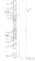
- Figure 4 illustrates the validation operation, reading, and erasing the markers in the registers E1, ...., E256, when the OL1 circuit shows that it is available, in sent the signal IDL to the control circuit EF.
- the DEB pointer is incremented regularly with each sub-cell period, and it provides a value that is equal to the TSTP time label of all cells whose timeout expires. In this exemplary embodiment, this value is identical to that the current TSTP time label provided by the generator TSG, because the total delay is chosen equal to the modulo, TSTPmax, of TSG generator. All time value labels greater than or equal to the value of the DEB pointer correspond to cells whose timeout has expired and which are therefore authorized to be issued. Because of the cyclical scanning of the values 0 to TSTPmax, we must also consider the values between O and the value of the END pointer.
- the FIN and DEB pointers validate the logic circuits F132, ..., F256, F1, F2, F3.
- the circuits Logics F1 to F256 can therefore only read the content of registers E1, E2, E3, E132, ..., E256, not shaded in Figure 4. In this reading area, they can detect a marker in the E132 register and a marker in the E1 register, for example. They determine that the highest ranking marker is the one contained in register 132.
- the coder COD therefore provides a TSTP 'time label equal to 132 in this example.
- the width Lo of the domain where the markers can be validly read must be less than or equal to:
- TSTPmax -Dmax + Dmin where Dmax is the maximum duration of transit in the switching network, and where Dmin is the duration minimum transit.
- TSTPmax-Lo the difference between the values initialization of pointers DEB and FIN must therefore be less at Dmax-Dmin.
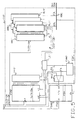
- Figure 5 shows the block diagram of the unit CU2 command of a second embodiment of the device according to the invention allowing the diffusion of a cell towards several outputs of the node.
- the unique OA exit address is replaced by a binary word OM comprising a number of bits equal to number N of outputs.
- a waiting cell memory, VIM2 replaces VIM1 and stores TSTP-OM identifiers instead of TSTP-OA identifiers.
- This memory can be read two ways: either by the content, like VIM1 memory, or by an address applied to the ad entry.
- Logic request circuits RL1 ', ..., RLN' provide identifiers of cells to be transmitted, TSTP '- OM', in which TSTP 'is still a time label value designating at least one cell whose time has expired, and where OM ' is a word of N bits among which a single bit has the value 1.
- the rank of this bit denotes a single output that is available.
- the VIM2 memory has a comparison input ci, but it works a little differently from the VIM1 memory described previously with reference to FIG. 2, because the comparison must relate to the field TSTP 'and to the only non-zero bit in OM'.
- the OM field bits in each TSTP - OM word must be masked by the bits of the OM 'field of TSTP' - OM 'before compare the TSTP identifier '- OM' and each pending cell identifier, TSTP - OM, stored in VIM2 memory.
- the direct link LC of circuit CU1 is replaced by the logic circuit LC 'added to zero a bit of the field OM in each TSTP - OM identifier which is detected by the comparison, in order to store in VIM2 memory the fact that a exit was served.
- the LC 'circuit has: an input connected to a common output of the logic request circuits RL1 ', ..., RLN ', to receive the TSTP identifier' - OM 'from cells to find; an input connected to the output of the arbitration circuit FF0 providing the RA address of an identifier found in memory VIM2; an output to retransmit this RA address to the circuit FMM2 management, when this address is released; a connected outlet at the data input, wd, from VIM2 memory: and an output linked to the comparison input ci of the VIM2 memory.
- the request logic circuit RL1 'of this output provides the VIM2 memory, via logic circuit LC ', the identifier: TSTP1-00001000.
- VIM2 memory contains at minus a pending cell identifier equal to TSTP1 - 00001100.
- This identifier means that there is a cell in hold, whose timeout has expired and which must be issued on the third and fourth exit.
- a first search by comparison with TSTP1 - 00001100 leads the VIM2 memory and the FF0 'circuit to be supplied the RA address of this pending cell identifier.
- the cell corresponding to this RA address is sent on the fourth exit.
- the LC 'circuit memorizes this fact by reading the identifier TSTP1- 00001100 at the address RA in the memory VIM2, then re-entering it in the modified form: TSTP1-00000100, at address RA in VIM2 memory.
- This identifier modified indicates that the third outlet remains to be served.
- the corresponding request circuit RL3 ' supplies to the memory VIM2, via the logic circuit LC ', a cell identifier to be transmitted TSTP1-00000100.
- a second search by comparison with this identifier leads the VIM2 memory and circuit FF0 'to supply the RA address again, which contains the modified identifier TSTP1-00000100.
- the LC 'circuit memorizes this fact by the following process: First of all, it obtains the identifier TSTP1-00000100 by reading at address RA in VIM2 memory and then rewriting it to the RA address in a modified form: TSTP1-00000000 which indicates that all the destination outlets have been served and which do not can no longer give a positive result in a search higher. The location can be reused. The LC 'circuit then transmits the address RA to the FMM2 circuit for managing free places.
- the arbitration circuit FF0 ' provides a logic signal M playing the same role as in the CU1 circuit. If VIM2 memory contains several identifiers whose TSTP field has a value equal to that of the TSTP 'field of the cell identifier to send, and whose OM field contains a value of 1 for the bit corresponding to the bit of value 1 in the OM 'field, the signal M takes the value 1 to indicate to the requesting request circuit that there are at least two cells to emit on the output corresponding, and this request circuit repeats sending the same cell identifier to be retrieved, until the signal M returns to the value 0.
- An alternative embodiment therefore consists in assigning a TSTP time tag to each cell leaving the network SN, instead of assigning it as input to the SN network.
- the TSG time label generator is different. It comprises another clock defining time intervals of duration constant equal to a sub-cell period; and a counter modulo TSTP max. But it also includes: known means for estimate the transit time of each cell through the network SN; means to subtract this estimate from the content of the counter; and means for adding to the result the duration of the total delay that each cell must undergo. The result of this calculation constitutes the value of the TSTP label indicating the time interval when the cell timeout expires. It can be used exactly like the TSTP label value assigned as input to the SN network.
- the time unit is preferably chosen equal to the sub-cell period because the duration of each cell is at least equal to a sub-cell period but it is possible to use a smaller unit of time.
Abstract
Description
L'invention concerne un dispositif de reséquencement pour un noeud d'un système de commutation de cellules. Elle concerne plus particulièrement les systèmes de commutation dans lesquels les cellules ont une longueur variable, chaque cellule pouvant être constituée d'un nombre variable de sous-cellules ayant une longueur fixe.The invention relates to a resequencing device for a node of a cell switching system. It concerns more particularly switching systems in which the cells have a variable length, each cell can be consisting of a variable number of sub-cells having a length fixed.
Chaque fois que ces cellules transitent à travers un noeud d'un système de commutation elles subissent chacune un retard variable en fonction du chemin suivi dans le réseau de commutation que comporte ce noeud. Les sous-cellules d'une même cellule sont liées de telle sorte qu'elles suivent un même chemin et subissent un même retard. A la sortie du réseau de commutation, les sous-cellules d'une même cellule ont donc conservé leur ordre initial, par contre les cellules n'ont pas toujours conservé leur ordre initial à cause de la dispersion des retards. Un dispositif de reséquencement a pour fonction de remettre ces cellules dans leur ordre initial.Whenever these cells pass through a node of a switching system they each undergo a variable delay depending on the path followed in the switching network that comprises this knot. The sub-cells of the same cell are linked in such a way so that they follow the same path and experience the same delay. AT the output of the switching network, the sub-cells of the same cells have therefore kept their initial order, however cells have not always kept their original order due to the dispersion of delays. A resequencing device has for function to put these cells back in their original order.
La publication de brevet européen n°0 438 415 (Alcatel NV) décrit un procédé de reséquencement consistant à retarder chaque cellule d'un retard déterminé de telle façon que le retard total imposé par le réseau de commutation et par le dispositif de reséquencement ait une valeur sensiblement constante pour toutes les cellules, cette valeur étant généralement choisie supérieure au retard maximal que peut créer le réseau de commutation. Si le retard total est choisi inférieur à la valeur maximale du retard que peut créer le réseau de commutation, la probabilité d'une pertubation de l'ordre initial n'est pas nulle, et est fonction de la valeur choisie pour le retard total. Ce procédé connu comporte deux variantes.European patent publication No. 0 438 415 (Alcatel NV) describes a resequencing method of delaying each delay cell determined so that the total delay imposed by the switching network and by the resequencing has a substantially constant value for all cells, this value generally being chosen greater than the delay maximum that the switching network can create. If the total delay is chosen less than the maximum value of the delay that the switching network, the probability of a disturbance of the order initial is not zero, and is a function of the value chosen for the total delay. This known process has two variants.
Une première variante consiste à : associer à chaque cellule entrant dans le réseau de commutation une étiquette temporelle qui indique à quel instant la cellule a pénétré dans le réseau de commutation; à extraire l'étiquette temporelle de chaque cellule sortant du réseau de commutation; à stocker chaque cellule sortant du réseau, jusqu'à ce que l'heure indiquée par le générateur d'étiquettes temporelles soit égale à l'heure indiquée dans l'étiquette temporelle de la cellule, plus le retard total choisi; et alors autoriser l'émission de la cellule sur une sortie du dispositif de reséquencement. L'émission est effectivement réalisé sitôt que la sortie à laquelle la cellule et destinée est disponible.A first variant consists in: associating with each cell entering the switching network a time tag which indicates when the cell entered the network of switching; to extract the time label from each cell leaving the switching network; to store each cell leaving the network, until the time indicated by the label generator is equal to the time indicated in the time label of the cell, plus the total delay chosen; and then allow the emission of the cell on an output of the resequencing. The program is actually produced as soon as the output at which the cell and intended is available.
Selon cette variante, l'ordre initial des cellules est reconstitué sans avoir à mesurer ou à estimer le retard de transit de chaque cellule à travers le réseau de commutation. Par contre, l'heure fournie par le générateur d'étiquettes temporelles doit être disponible dans un dispositif situé à l'entrée du réseau pour attribuer des étiquettes temporelles, et doit être disponible simultanément dans un dispositif de reséquencement situé à la sortie du réseau, pour autoriser l'émission de chaque cellule à un instant convenable.According to this variant, the initial order of the cells is reconstructed without having to measure or estimate the transit delay of each cell across the switching network. However, the time provided by the time label generator must be available in a device located at the entrance to the network for assign time tags, and must be available simultaneously in a resequencing device located at the output of the network, to authorize the emission of each cell at a time suitable.
Selon une autre variante de ce procédé connu, il consiste à associer à chaque cellule sortant du réseau une étiquette dont la valeur est une estimation du retard subi par la cellule au cours de son transit à travers le réseau; et à faire subir à chaque cellule un retard supplémentaire de durée égale à la différence entre la valeur prédéterminée du retard total et la valeur estimée du retard de transit dans le réseau, cette dernière étant lue dans l'étiquette associée à chaque cellule. Cette variante présente l'avantage de ne pas nécessiter un dispositif associant des étiquettes temporelles aux cellules arrivant aux entrées du réseau de commutation.According to another variant of this known method, it consists to associate with each cell leaving the network a label whose value is an estimate of the delay experienced by the cell during its transit through the network; and subject each cell to a additional delay of duration equal to the difference between the value predetermined total delay and the estimated value of the delay transit in the network, the latter being read in the label associated with each cell. This variant has the advantage of not not require a device associating time labels with cells arriving at the inputs of the switching network.
Cette demande de brevet décrit aussi un dispositif de reséquencement mettant en oeuvre la première variante du procédé mentionné ci-dessus, pour des cellules constituées chacune d'un nombre variable de sous-cellules ayant chacune une longueur fixe. Chaque sortie d'un noeud est munie d'un exemplaire de ce dispositif. Ce dispositif comporte :
- un générateur de premières étiquettes temporelles, fournissant une valeur incrémentée d'une unité pour chaque intervalle de temps correspondant à une sous-cellule, avec une durée de cycle au moins égale au retard total prédéterminé pour retarder uniformément toutes les cellules;
- une mémoire tampon ayant une entrée couplée à une entrée du dispositif de reséquencement, et ayant une sortie couplée à une sortie du dispositif de reséquencement; chaque emplacement de cette mémoire ayant une capacité égale à une sous-cellule;
- un circuit de gestion de cette mémoire tampon, pour fournir des adresses d'emplacements libres dans cette mémoire tampon et pour y stocker respectivement les sous-cellules de chaque cellule reçue par le dispositif de reséquencement;
- un pointeur de lecture-écriture associé à la mémoire tampon;
- une mémoire d'adresses ayant des emplacements correspondant respectivement aux diverses valeurs possibles de l'étiquette temporelle; chaque emplacement de cette mémoire d'adresses stockant un pointeur de début de liste et un pointeur de fin de liste qui sont respectivement les adresses, dans la mémoire tampon, de la première et de la dernière sous-cellule d'une suite contenant toutes les cellules ayant une même étiquette temporelle;
- une mémoire de liens, ayant le même ensemble d'adresses que la mémoire tampon, pour mémoriser des liens entre les adresses de toutes les sous-cellules ayant une même étiquette temporelle, et pour mémoriser des liens entre les adresses de sous-cellules appartenant à des cellules devant être émises successivement;
- un pointeur d'écriture associé à cette mémoire d'adresses pour stocker dans chaque emplacement la première adresse et la dernière adresse d'une liste d'adresses d'emplacements de la mémoire tampon, contenant toutes les sous-cellules de toutes les cellules ayant la même étiquette temporelle;
- un pointeur de lecture associé à la mémoire d'adresses, ayant un fonctionnement cyclique, pour lire successivement les contenus des emplacements de cette mémoire d'adresses, afin de lire des sous-cellules dans la mémoire tampon à des adresses correspondant à des étiquettes temporelles croissant de manière régulière.
- a first time tag generator, providing a value incremented by one for each time interval corresponding to a sub-cell, with a cycle time at least equal to the predetermined total delay to uniformly delay all cells;
- a buffer memory having an input coupled to an input of the resequencing device, and having an output coupled to an output of the resequencing device; each location of this memory having a capacity equal to a sub-cell;
- a circuit for managing this buffer memory, for supplying addresses of free locations in this buffer memory and for storing therein respectively the sub-cells of each cell received by the resequencing device;
- a read-write pointer associated with the buffer memory;
- an address memory having locations corresponding respectively to the various possible values of the time label; each location in this address memory storing a start of list pointer and an end of list pointer which are respectively the addresses, in the buffer memory, of the first and of the last sub-cell of a sequence containing all the cells with the same time tag;
- a link memory, having the same set of addresses as the buffer memory, for memorizing links between the addresses of all the sub-cells having the same time label, and for memorizing links between the addresses of sub-cells belonging to cells to be emitted successively;
- a write pointer associated with this address memory for storing in each location the first address and the last address of a list of addresses of locations in the buffer memory, containing all the sub-cells of all the cells having the same time label;
- a read pointer associated with the address memory, having a cyclic operation, for successively reading the contents of the locations of this address memory, in order to read sub-cells in the buffer memory at addresses corresponding to time labels growing steadily.
Lorsque le délai expire pour une suite de cellules ayant une étiquette temporelle donnée, c'est-à-dire lorsque l'heure indiquée par le générateur d'étiquettes est égale à la somme de l'étiquette temporelle donnée et du retard total prédéterminé, la première et la dernière adresse de stockage de cette suite sont lues dans l'emplacement de la mémoire d'adresses correspondant à cette étiquette temporelle. Puis la mémoire de liens fournit la suite complète d'adresses, et permet donc de lire dans la mémoire tampon toutes les sous-cellules de toutes les cellules ayant l'étiquette temporelle considérée. Ces cellules sont lues dans un ordre qui est celui défini par les liens dans la mémoire de liens, mais cet ordre n'a pas d'importance puisque toutes ces cellules ont la même étiquette temporelle et sont adressées à une même sortie. La mémoire de liens est utilisée en outre pour enchaíner dans une même file d'attente les différentes suites de sous-cellules de cellules ayant des étiquettes temporelles successives, ce qui assure leur émission en bon ordre. Cet enchaínement est réalisé en faisant correspondre par la mémoire de liens la fin de la suite d'adresses de sous-cellule d'une cellule avec le début de la suite d'adresses de sous-cellule de la cellule à émettre ensuite.When the time expires for a series of cells having a given time label, i.e. when the time indicated by the label generator is equal to the sum of the label given time and the total predetermined delay, the first and the last storage address of this suite are read in the location of the address memory corresponding to this label time. Then the link memory provides the complete suite addresses, and therefore makes it possible to read in the buffer memory all the sub-cells of all cells with the time label considered. These cells are read in an order which is that defined by the links in the link memory, but this order has no of importance since all these cells have the same label and are addressed to the same output. Memory links is also used to chain in the same queue the different sequences of cell sub-cells with labels successive times, which ensures their emission in good order. This linking is achieved by matching by the memory of links the end of the sub-cell address sequence of a cell with the start of the cell sub-cell address sequence at then issue.
Ce dispositif a un premier inconvénient qui est de ne pouvoir remettre en ordre des cellules arrivant sur une même entrée et étant destinées à plusieurs sorties, en particulier lorsqu'une même cellule doit être diffusée sur plusieurs sorties. Cette impossibilité découle du principe de fonctionnement de ce dispositif connu, parce qu'il nécessite de stocker, dans la mémoire d'adresses, à chaque emplacement, une adresse de début de suite d'adresses et une adresse de fin de suite d'adresses de sous-cellules; et qu'il nécessite de lier par une mémoire de liens toutes les sous-cellules qui devront ultérieurement être émises sur une même sortie.This device has a first drawback which is that it does not ability to re-order cells arriving at the same entrance and being intended for several outputs, in particular when the same cell must be broadcast on several outputs. This impossibility follows from the operating principle of this known device, because that it needs to be stored in the address memory each time location, address start address, and address end of sequence of sub-cell addresses; and that it requires link all the sub-cells which will have to be linked subsequently be issued on the same output.
Ce dispositif connu a un second inconvénient qui est de ne pas permettre la diffusion d'une cellule vers plusieurs sorties.This known device has a second drawback which is that it does not not allow the diffusion of a cell towards several exits.
Ce dispositif connu a en outre pour inconvénient de ne pas permettre de grandes longueurs de cellule. Chaque emplacement de la mémoire d'adresses correspond à une unité de temps du générateur qui délivre les étiquettes temporelles. Cette unité de temps est égale à la durée d'une sous-cellule. Le générateur d'étiquettes temporelle n'a pas une capacité infinie. Il délivre donc des valeurs étiquettes identiques périodiquement. Chaque emplacement de la mémoire d'adresses est lu avec une période constante, au plus égale à la période du générateur d'étiquettes temporelles. Au moment de la lecture d'un emplacement, il faut que la constitution de la liste soit terminée, pour qu'une adresse de fin de liste puisse être lue valablement dans l'emplacement considéré. La période du générateur d'étiquettes temporelles limite donc le nombre de sous-cellules correspondant à cette liste, et finalement limite le nombre de sous-cellules que peut comporter chaque cellule.This known device also has the disadvantage of not allow long cell lengths. Each location of the address memory corresponds to a time unit of the generator which issues time tags. This unit of time is equal to the duration of a sub-cell. The time label generator did not not an infinite capacity. It therefore delivers label values identical periodically. Each location in the address memory is read with a constant period, at most equal to the period of time label generator. When reading a location, the constitution of the list must be completed, so that an end of list address can be validly read in the location considered. The period of the label generator therefore limit the number of sub-cells corresponding to this list, and finally limits the number of sub-cells that can have each cell.
Par ailleurs, il n'est pas possible d'augmenter indéfiniment la période du générateur d'étiquettes temporelles car cela nécessite d'augmenter le nombre de bits adjoints à chaque cellule pour constituer une étiquette temporelle.Furthermore, it is not possible to increase indefinitely the period of the time label generator because this requires increasing the number of bits attached to each cell to constitute a time label.
Un premier but de l'invention est de proposer un dispositif de reséquencement permettant la diffusion d'une cellule d'une entrée vers plusieurs sorties prédéterminées, du dispositif de reséquencement. Un second but de l'invention est de proposer un dispositif de reséquencement pouvant être adapté plus facilement pour qu'il accepte des cellules composées d'un grand nombre de sous-cellules.A first object of the invention is to propose a resequencing device allowing the diffusion of a cell from one input to several predetermined outputs, from the resequencing. A second object of the invention is to propose a resequencing device which can be adapted more easily for that it accepts cells composed of a large number of subcells.
L'objet de l'invention est un dispositif de reséquencement pour un noeud d'un système de commutation de cellules, chaque cellule étant constituée d'un nombre variable de sous-cellules ayant une longueur fixe, ce noeud comportant un réseau de commutation transmettant les cellules avec des premiers retards variables, toutes les sous-cellules d'une même cellule subissant un même premier retard; ce dispositif de reséquencement comportant des moyens pour stocker toutes les cellules ayant été transmises à travers le réseau de commutation, puis les émettre sur au moins une sortie du dispositif de reséquencement, après l'expiration de divers délais d'attente constituant des seconds retards tels que, pour chaque cellule, la somme du premier et du second retard est égale à une valeur prédéterminée sensiblement identique pour toutes les cellules; ces moyens comportant :
- une mémoire tampon pour stocker les sous-cellules de chaque cellule reçue par le dispositif de reséquencement;
- une mémoire d'adresses pour mémoriser l'adresse, de la mémoire tampon, contenant la la première sous-cellule de chaque cellule;
- des moyens pour retrouver l'adresse, de la mémoire d'adresses, contenant la première sous-cellule d'une cellule, lorsque le délai d'attente de cette dernière a expiré, et qu'une sortie qui doit émettre cette cellule est disponible;
- une mémoire dite de cellules en attente, accessible par son contenu, pour mémoriser un identificateur dit de cellule en attente, lorsqu'une cellule est stockée dans la mémoire tampon; cet identificateur étant stocké à une adresse identique à celle où est stockée, dans la mémoire d'adresses, l'adresse de la première sous-cellule; et cet identificateur étant constitué : de l'identité d'un intervalle de temps au cours duquel expire le délai d'attente de cette cellule, et de l'identité d'au moins une sortie sur laquelle elle doit être émise;
- des mémoires dites de marqueurs, associées respectivement aux sorties du noeud, pour mémoriser un marqueur lorsqu'une cellule est stockée dans la mémoire tampon, chaque marqueur mémorisé identifiant un intervalle de temps au cours duquel expire le délai d'attente d'au moins une cellule destinée à la sortie associée à la mémoire de marqueurs considérée;
- des moyens associés respectivement aux mémoires de marqueurs pour lire et effacer le marqueur le plus ancien parmi les marqueurs correspondant à des délais d'attente ayant expiré, lorsque la sortie correspondante est disponible; et pour fournir un identificateur de cellule à émettre constitué de l'identité de l'intervalle de temps et de l'identité de la sortie correspondant à ce marqueur lu;
- des moyens pour appliquer cet identificateur de cellule à émettre à une entrée de comparaison de la mémoire de cellules en attente, cette mémoire fournissant alors les adresses de tous les identificateurs de cellule en attente correspondant à cet identificateur de cellule à émettre; et pour libérer les emplacements de cette mémoire correspondant aux cellules qui ne doivent plus être émises;
- des moyens pour appliquer successivement à une entrée d'adresse de la mémoire de premières sous-cellules, chaque adresse fournie par la mémoire de cellules en attente, et y lire une adresse de première sous-cellule.
- a buffer memory for storing the sub-cells of each cell received by the resequencing device;
- an address memory for storing the address, of the buffer memory, containing the first sub-cell of each cell;
- means for retrieving the address, from the address memory, containing the first sub-cell of a cell, when the waiting time of the latter has expired, and an output which must transmit this cell is available ;
- a so-called waiting cell memory, accessible by its content, for storing a so-called waiting cell identifier, when a cell is stored in the buffer memory; this identifier being stored at an address identical to that where the address of the first sub-cell is stored in the address memory; and this identifier being made up of: the identity of a time interval during which the waiting time of this cell expires, and the identity of at least one output on which it must be sent;
- so-called marker memories, respectively associated with the outputs of the node, for storing a marker when a cell is stored in the buffer memory, each memorized marker identifying a time interval during which the waiting period of at least one expires cell for the output associated with the marker memory considered;
- means respectively associated with the marker memories for reading and erasing the oldest marker among the markers corresponding to waiting times having expired, when the corresponding output is available; and to provide a cell identifier to be transmitted consisting of the identity of the time interval and the identity of the output corresponding to this marker read;
- means for applying this cell identifier to be transmitted to a comparison input of the waiting cell memory, this memory then providing the addresses of all the waiting cell identifiers corresponding to this cell identifier to be sent; and to free the locations of this memory corresponding to the cells which must no longer be transmitted;
- means for successively applying to an address entry of the memory of first sub-cells, each address supplied by the memory of waiting cells, and reading there an address of first sub-cell.
Le dispositif ainsi caractérisé est compatible avec une diffusion parce qu'il est associé à l'ensemble des sorties d'un noeud et parce que la mémoire de cellules en attente stocke des identificateurs qui peuvent contenir chacun plusieurs identités de sortie destinataire.The device thus characterized is compatible with a diffusion because it is associated with all the outputs of a node and because the pending cell memory stores identifiers which can each contain several identities of recipient output.
D'autre part, il est plus facile à réaliser pour des cellules de grandes longueurs car l'identificateur d'une cellule en attente peut être mémorisé dans cette mémoire sans attendre que toutes les sous-cellules de cette cellule aient été effectivement reçues par le noeud. Les premières sous-cellules d'une cellule peuvent donc être émises sur une sortie avant même que les dernières sous-cellules aient été reçues.On the other hand, it is easier to carry out for long cells because the identifier of a cell in wait can be stored in this memory without waiting for all the sub-cells of this cell were actually received by the knot. The first sub-cells of a cell can therefore be emitted on an output even before the last sub-cells have been received.
Selon un mode de réalisation du dispositif selon
l'invention, il est caractérisé en ce que les mémoires de marqueurs
comportent, pour chaque sortie, une suite de registres; chaque
registre étant susceptible de mémoriser un seul marqueur, et le nombre
de registres étant égal au nombre des identités utilisables pour
identifier des intervalles de temps;
- des moyens pour lire les marqueurs correspondant aux intervalles de temps les plus anciens;
- des moyens reliés à tous les registres, pour fournir un identificateur de cellule à émettre constitué : de l'identité de l'intervalle de temps le plus ancien parmi ceux correspondant aux marqueurs lus; et de l'identité de ladite sortie;
- des moyens pour effacer le marqueur correspondant à l'intervalle de temps le plus ancien, parmi les marqueurs lus, lorsque toutes les cellules correspondant à cet identificateur de cellule à émettre ont été retrouvées dans la mémoire de cellules en attente.
- means for reading the markers corresponding to the oldest time intervals;
- means connected to all the registers, for supplying a cell identifier to be transmitted consisting of: the identity of the oldest time interval among those corresponding to the markers read; and the identity of said outlet;
- means for erasing the marker corresponding to the oldest time interval, among the markers read, when all the cells corresponding to this cell identifier to be emitted have been found in the memory of waiting cells.
Un mode de réalisation, permettant la diffusion d'une cellule d'une entrée vers plusieurs sorties du dispositif de reséquencement, est caractérisé en ce que :
- pour chaque cellule devant être émise par plusieurs sorties, un identificateur de cellule en attente identifie chacune des sorties sur lesquelles elle doit être émise;
- chaque identificateur de cellule à émettre identifie une seule sortie disponible;
- retrouver dans la mémoire de cellules en attente, successivement chaque identificateur de cellule en attente, contenant l'identité de la sortie disponible identifiée par l'identificateur de cellule à émettre;
- lire dans cette mémoire chaque identificateur, de cellule en attente, ainsi retrouvé;
- émettre la cellule correspondante sur ladite sortie;
- réinscrire cet identificateur à la même adresse dans la mémoire de cellules en attente, après avoir supprimé dans cet identificateur l'identité de la sortie où la cellule a été émise, pour mettre à jour cet identificateur de cellule en attente.
- for each cell to be transmitted by several outputs, a pending cell identifier identifies each of the outputs on which it must be transmitted;
- each cell identifier to be transmitted identifies a single available output;
- find in the waiting cell memory, successively each waiting cell identifier, containing the identity of the available output identified by the cell identifier to be sent;
- read in this memory each identifier, of cell pending, thus found;
- emitting the corresponding cell on said output;
- re-register this identifier at the same address in the waiting cell memory, after having deleted in this identifier the identity of the output where the cell was emitted, to update this waiting cell identifier.
L'invention sera mieux comprise et d'autres détails apparaítront à l'aide de la description ci-dessous et des figures l'accompagnant :
- la figure 1 représente un schéma synoptique commun à un premier et un deuxième exemple de réalisation du dispositif selon l'invention, raccordé à un réseau de commutation, pour constituer un noeud d'un système de commutation de cellules;
- la figure 2 représente un schéma synoptique plus détaillé du premier exemple de réalisation, qui ne convient que pour des cellules destinées à une sortie unique;
- la figure 3 représente le schéma synoptique d'une partie du premier exemple de réalisation ;
- la figure 4 illustre le fonctionnement de cette partie du premier exemple de réalisation;
- la figure 5 représente un schéma synoptique d'une partie du deuxième exemple de réalisation, permettant une diffusion d'une entrée vers plusieurs sorties.
- FIG. 1 represents a block diagram common to a first and a second embodiment of the device according to the invention, connected to a switching network, to constitute a node of a cell switching system;
- FIG. 2 represents a more detailed block diagram of the first exemplary embodiment, which is only suitable for cells intended for a single output;
- FIG. 3 represents the block diagram of part of the first exemplary embodiment;
- Figure 4 illustrates the operation of this part of the first embodiment;
- FIG. 5 represents a block diagram of part of the second exemplary embodiment, allowing diffusion of an input to several outputs.
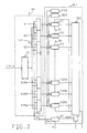
La figure 1 représente un noeud d'un réseau de télécommunications à mode de transfert asynchrone, comportant un réseau de commutation SW et un exemple de réalisation, RU, du dispositif de reséquencement selon l'invention. Ce noeud comporte M entrées IN1,...,INM, et N sorties OU1,...,OUN. Cet exemple de réalisation du dispositif de reséquencement RU comporte :
- M circuits étiquetteurs IC1,...,ICM, ayant chacun : une entrée reliée respectivement à une entrée IN1,...,INM du noeud, une sortie reliée respectivement à l'une des N entrées du réseau de commutation SW, et une entrée commune;
- M circuits d'entrée IL1,...,ILM ayant chacun : une entrée reliée respectivement à l'une des M sorties du réseau de commutation SW, et une sortie reliée à un bus TDM1 à multiplexage temporel;
- un circuit HP de traitement des en-têtes de cellule, ayant une première entrée reliée au bus TDM1;
- une unité de commande CU qui sera détaillée plus loin et qui comporte une première entrée reliée respectivement à une première sortie du circuit HP de traitement des en-têtes;
- un générateur d'étiquettes temporelles, TSG, ayant une sortie reliée à l'entrée commune des circuits étiquetteurs IC1,...,ICM, ; ce générateur étant constitué d'une horloge et d'un compteur, non représentés, pour fournir une valeur d'étiquette temporelle incrémentée d'une unité pour chaque intervalle de temps correspondant à une sous-cellule, de O à TSTPmax, modulo TSTPmax;
- une mémoire tampon BM associée à une unité de gestion de mémoire tampon BMMU, cet ensemble ayant : une entrée reliée à une deuxième sortie du circuit HP de traitement d'en-têtes, une sortie reliée à une deuxième entrée du circuit HP, et une entrée-sortie reliée à un bus TDM2 à multiplexage temporel;
- une mémoire FSAM appelée mémoire d'adresses, ayant : une entrée de données, di, reliée à une troisième sortie du circuit HP, une entrée d'adresse ad reliée à une sortie de l'unité CU, et une sortie do reliée à une deuxième entrée de l'unité CU;
- N circuits de sorties OL1,...,OLN ayant chacun : une entrée-sortie reliée au bus TDM2, une sortie reliée respectivement à l'une des sorties OU1,...,OUN du noeud, et une entrée-sortie reliée à un bus RQB, lui-même relié à une entrée-sortie de l'unité de commande CU.
- M labeling circuits IC1, ..., ICM, each having: an input connected respectively to an input IN1, ..., INM of the node, an output connected respectively to one of the N inputs of the switching network SW, and a common entrance;
- M input circuits IL1, ..., ILM each having: an input connected respectively to one of the M outputs of the switching network SW, and an output connected to a TDM1 bus with time multiplexing;
- an HP circuit for processing the cell headers, having a first input connected to the TDM1 bus;
- a control unit CU which will be detailed below and which has a first input connected respectively to a first output of the HP circuit for processing the headers;
- a generator of time labels, TSG, having an output connected to the common input of the labeling circuits IC1, ..., ICM,; this generator consisting of a clock and a counter, not shown, for supplying a time label value incremented by one for each time interval corresponding to a sub-cell, from O to TSTPmax, modulo TSTPmax;
- a buffer memory BM associated with a buffer memory management unit BMMU, this assembly having: an input connected to a second output of the HP header processing circuit, an output connected to a second input of the HP circuit, and a input-output connected to a TDM2 bus with time multiplexing;
- a memory FSAM called address memory, having: a data input, di, connected to a third output of the HP circuit, an address input ad connected to an output of the unit CU, and an output do connected to a second input of the CU unit;
- N output circuits OL1, ..., OLN each having: an input-output connected to the TDM2 bus, an output connected respectively to one of the outputs OU1, ..., OUN of the node, and an input-output connected to an RQB bus, itself connected to an input / output of the control unit CU.
Les entrées IN1,...,INM reçoivent des cellules de longueur fixe ou variable, constituées chacune de sous-cellules ayant toutes le même nombre de bits et la même durée, cette durée étant appelée période de sous-cellule. Le dispositif selon l'invention est particulièrement adapté pour traiter des cellules à longueur variable. Ces cellules sont commutées dans le réseau de commutation SW en routant toutes les sous-cellules d'une même cellule par un même chemin et en maintenant la continuité de la cellule, c'est-à-dire sans entrelacer des sous-cellules appartenant à des cellules différentes. Ceci permet d'attribuer une étiquette temporelle unique pour l'ensemble des sous-cellules constituant une cellule. Cette étiquette temporelle indique l'intervalle de temps pendant lequel la première sous-cellule de la cellule considérée est reçue à l'une des entrées IN1,...,INM.Inputs IN1, ..., INM receive length cells fixed or variable, each consisting of sub-cells all having the same number of bits and the same duration, this duration being called sub-cell period. The device according to the invention is particularly suitable for treating cells of variable length. These cells are switched in the switching network SW in routing all the sub-cells of the same cell by the same path and maintaining the continuity of the cell, that is to say without interweave sub-cells belonging to different cells. This allows you to assign a unique time label for the set of sub-cells constituting a cell. This label temporal indicates the time interval during which the first sub-cell of the considered cell is received at one of the inputs IN1, ..., MNI.
Cette étiquette permet de reséquencer les cellules sortant du réseau de commutation SW : la première sous-cellule est autorisée à sortir du noeud lorsque son délai d'attente a expiré, c'est-à-dire au cours de l'intervalle de temps où le générateur TSG indique une heure égale à la somme de la valeur de l'étiquette temporelle qui fut attribuée à la cellule, et d'une valeur fixée. Mais il y a une condition supplémentaire pour que la cellule soit émise : la sortie à laquelle est destinée cette cellule, doit être disponible. Sinon, il faut que la cellule considérée attende encore jusqu'à ce que cette sortie soit disponible.This label allows resequencing outgoing cells of the SW switching network: the first sub-cell is authorized to leave the node when its waiting time has expired, that is to say at during the time interval where the TSG generator indicates an hour equal to the sum of the value of the time label which was assigned to the cell, and a fixed value. But there is a additional condition for the cell to be emitted: the output at which this cell is intended for, must be available. Otherwise, it the cell in question must wait again until this output is available.
Chaque sous-cellule commence par deux bits appelés champ de contrôle de sous-cellule. Dans la première sous-cellule de chaque cellule, ces deux bits ont pour valeur 11 par exemple. Dans toutes les autres sous-cellules, sauf la dernière, ces deux bits ont pour valeur 00 par exemple. Dans la dernière sous-cellule, ces deux bits ont pour valeur 01 par exemple. La première sous-cellule comporte en outre un champ appelé en-tête de contrôle de cellule. Ce champ contient notamment l'identité de la sortie qui doit émettre cette cellule, ou de plusieurs sorties dans le cas d'une diffusion. Les autres bits des sous-cellules transmettent des données.Each sub-cell begins with two bits called field sub-cell control. In the first sub-cell of each cell, these two bits have the value 11 for example. In all other sub-cells, except the last one, these two bits have the value 00 for example. In the last sub-cell, these two bits have for value 01 for example. The first sub-cell further includes a field called cell control header. This field contains in particular the identity of the output which must emit this cell, or of several outputs in the case of a broadcast. The other bits of sub-cells transmit data.
Les étiquetteurs IC1,...,ICM ont pour fonction d'insérer dans le champ de contrôle de cellule, de chaque cellule, une étiquette temporelle fournie par le générateur TSG à l'instant où la première sous-cellule de cette cellule est reçue par le noeud. Cette étiquette temporelle TSTP indique l'intervalle de temps au cours duquel expirera le délai d'attente de la cellule. Elle est déterminée en fonction du contenu du compteur de TSG à l'instant où cette cellule arrive, et en fonction du retard total prédéterminé que chaque cellule doit subir. Dans un mode de réalisation préférentiel, le modulo TSTPmax, du compteur est choisi égal à ce retard total prédéterminé, la valeur de l'étiquette temporelle TSTP est alors numériquement égale à la valeur fournie par le compteur, à cause du modulo TSTPmax.The function of labels IC1, ..., ICM is to insert in the cell control field, of each cell, a label time provided by the TSG generator at the time when the first sub-cell of this cell is received by the node. This label time TSTP indicates the time interval during which will expire the cell's waiting time. It is determined according to the contents of the TSG counter at the moment this cell arrives, and as a function of the predetermined total delay that each cell must undergo. In a preferred embodiment, the modulo TSTPmax, of the counter is chosen equal to this predetermined total delay, the value of the TSTP time label is then numerically equal to the value supplied by the meter, because of the TSTPmax modulo.
Quand l'un des circuits d'entrée IL1,....,ILM reçoit une cellule, il demande à l'unité de gestion BMMU des adresses libres pour stocker respectivement les sous-cellules de cette cellule dans la mémoire tampon BM. Afin d'optimiser l'utilisation de la mémoire tampon BM, les sous-cellules d'une même cellule ne sont pas stockées à des adresses consécutives mais à des adresses aléatoires. L'unité de gestion BMMU comporte notamment un circuit WRC de commande d'écriture et de lecture, stockant les adresses libres de la mémoire tampon BM au fur à mesure qu'elles sont libérées par l'émission de cellules, et comporte une mémoire de liens SLM stockant toutes les adresses des emplacements, de la mémoire tampon BM, stockant respectivement toutes les sous-cellules d'une même cellule. Chaque emplacement de la mémoire tampon a une capacité égale à une sous-cellule.When one of the input circuits IL1, ...., ILM receives a cell, it asks the BMMU management unit for free addresses for respectively store the sub-cells of this cell in the BM buffer memory. In order to optimize the use of the buffer memory BM, the sub-cells of the same cell are not stored at consecutive addresses but at random addresses. The unit of BMMU management includes a WRC write control circuit and read, storing the free addresses of the buffer memory BM at the as they are released by the emission of cells, and includes an SLM link memory storing all the addresses of locations, from the BM buffer, respectively storing all sub-cells of the same cell. Each memory location buffer has a capacity equal to a sub-cell.
La réalisation de la mémoire tampon BM et de l'unité de gestion BMMU est à la portée de l'Homme de l'Art car elle est décrite notamment dans la publication de brevet européen EP 0 441 787 (Alcatel NV). Préférentiellement, la mémoire tampon BM et la mémoire de liens SLM ont un même ensemble d'adresses pour faciliter la réalisation .The realization of the buffer memory BM and the unit of BMMU management is within the reach of the skilled person because it is described in particular in the publication of European patent EP 0 441 787 (Alcatel NV). Preferably, the BM buffer memory and the link memory SLM have the same set of addresses to facilitate implementation.
La demande émise par l'un des circuits d'entrée IL1,...,ILM est transmise par le bus TDM1, puis par le circuit de traitement d'en-têtes HP jusqu'à l'unité de gestion BMMU. Cette dernière attribue aux sous-cellules de la cellule considérée une suite d'emplacements libres de la mémoire tampon BM. Une suite d'adresses désignant ces emplacements libres est fournie par le circuit WRC. Des liens entre les adresses de cette suite sont constitués en mémorisant cette suite d'adresses dans la mémoire de liens SLM, à des adresses consécutives. L'unité de gestion BMMU fournit au circuit de traitement d'en-têtes, HP, une valeur FSA qui est la première adresse de cette suite d'adresses d'emplacements de la mémoire tampon BM. L'adresse FSA est retransmise sur la troisième sortie du circuit HP. Cette adresse FSA est inscrite dans la mémoire d'adresses FSAM dans un emplacement libre dont l'adresse est fournie par la sortie de l'unité CU.The request issued by one of the input circuits IL1, ..., ILM is transmitted by the TDM1 bus, then by the processing of HP headers up to the BMMU management unit. This last assigns to the sub-cells of the cell considered a sequence of free locations in the BM buffer memory. A series of addresses designating these free locations is provided by the WRC circuit. of the links between the addresses of this suite are formed by memorizing this sequence of addresses in the SLM link memory, at addresses consecutive. The BMMU management unit supplies the processing circuit of headers, HP, an FSA value which is the first address of this sequence of addresses of locations in the BM buffer memory. The FSA address is retransmitted on the third output of the HP circuit. This address FSA is stored in FSAM address memory in a location free whose address is provided by the output of the CU unit.
Cette adresse FSA permettra ultérieurement de retrouver toutes les sous-cellules de cette cellule dans la mémoire tampon BM : En utilisant cette adresse FSA, il est possible de lire, dans la mémoire de liens SLM, l'adresse d'une deuxième sous-cellule dans la mémoire-tampon BM. Puis, avec l'adresse de cette deuxième sous-cellule, il est possible de lire dans la mémoire de liens SLM l'adresse d'une troisième sous-cellule dans la mémoire tampon BM. Il est donc possible d'obtenir succesivement les adresses de toutes les sous-cellules d'une même cellule à partir d'une adresse FSA unique. Ces adresses permettent ensuite de lire les sous-cellules elles-mêmes, dans la mémoire tampon BM.This FSA address will allow later to find all sub-cells of this cell in the BM buffer: Using this FSA address, it is possible to read, in the SLM link memory, the address of a second sub-cell in the BM buffer. Then, with the address of this second sub-cell, it is possible to read in the memory of SLM links the address of a third sub-cell in the buffer BM. he it is therefore possible to successively obtain the addresses of all the sub-cells of the same cell from a single FSA address. These addresses then make it possible to read the sub-cells themselves, in the BM buffer.
Le circuit HP extrait, dans le champ de contrôle de cellule de la première sous-cellule de chaque cellule reçue, le champ contenant l'étiquette temporelle TSTP et un champ contenant l'identité de la sortie, ou des sorties, OU1,...,OUN, sur laquelle ou lesquelles la cellule doit être émise. The extracted HP circuit, in the control field of cell of the first sub-cell of each cell received, the field containing the TSTP time label and a field containing the identity the output, or outputs, OU1, ..., OUN, on which the cell must be issued.
Le premier exemple de réalisation, décrit plus loin, ne
convient que dans le cas où une cellule n'est destinée qu'à une
seule sortie. L'identité de la sortie unique destinée à émettre une
cellule est notée OA. Le circuit HP fournit simultanément à l'unité
de commande CU : l'étiquette temporelle TSTP, l'identité de sortie
OA, et la première adresse de sous-cellule FSA. Le second exemple
de réalisation convient dans le cas où une cellule est
destinée à plusieurs sorties, l'identité de ces sorties est notée
OM. Pour un dispositif à N sorties cette identité OM peut être un
mot de N bits où la valeur 1 est attribuée aux bits correspondant
aux sorties auxquelles la cellule est destinée. La valeur 0 est
attribuée aux autres bits.The first exemplary embodiment, described below, does not
only suitable if a cell is only intended for one
only exit. The identity of the single output intended to issue a
cell is denoted OA. The HP circuit simultaneously supplies the unit
CU command line: TSTP time label, exit identity
OA, and the first FSA sub-cell address. The second example
of realization is suitable in the case where a cell is
intended for several outings, the identity of these outings is noted
OM. For a device with N outputs this identity OM can be a
N-bit word where the
Le traitement de ces données par l'unité CU sera décrit en détail plus loin, en distinguant deux variantes de réalisation correspondant respectivement au premier et au second exemple de réalisation du dispositif selon l'invention.The processing of this data by the CU unit will be described in detail below, distinguishing two variant embodiments corresponding respectively to the first and second examples of realization of the device according to the invention.
Pour émettre une cellule, le fonctionnement de l'unité de commande CU est déclenché par les circuits de sortie OL1,...,OLN lorsque l'un de ces circuits de sortie est disponible, c'est-à-dire lorsqu'il a fini d'émettre une cellule. Il envoie sur le bus RQB un message noté IDL contenant l'identité de la sortie qui est disponible, et adressé à l'unité de commande CU. L'unité de commande CU détermine alors quelle cellule va être émise sur cette sortie. L'unité CU envoie, au circuit de sortie demandeur, l'adresse FSA' d'un emplacement, de la mémoire tampon BM, contenant la première sous-cellule d'une cellule. Le circuit de sortie demande ensuite à la mémoire tampon BM et à son unité de gestion BMMU, de lui fournir la suite complète des sous-cellules de cette cellule. Puis il l'émet sur sa sortie.To transmit a cell, the operation of the unit control unit CU is triggered by the output circuits OL1, ..., OLN when one of these output circuits is available, i.e. when it finishes emitting a cell. It sends on the RQB bus a message noted IDL containing the identity of the output which is available, and addressed to the CU control unit. The unit of CU command then determines which cell will be sent on this exit. The CU unit sends, to the requesting output circuit, the FSA 'address of a location, from the buffer BM, containing the first sub-cell of a cell. The output circuit then requests to the buffer memory BM and to its management unit BMMU, to provide it with the complete suite of sub-cells of this cell. Then it emits it on its exit.
La figure 2 représente le schéma synoptique de l'unité de commande CU1 du premier exemple de réalisation du dispositif de reséquencement selon l'invention, qui ne peut acheminer une cellule que vers une seule sortie parmi les N sorties OU1, ..., OUN. L'unité CU1 comporte essentiellement :
- une mémoire de cellules en attente, VIM1, qui est du type accessible par le contenu, et qui a le même ensemble d'adresses que la mémoire FSAM, et la mémoire tampon BM;
- N mémoires de marqueurs, AM1, ...,AMN respectivement associés aux sorties OU1, ...,OUN;
- N circuits logiques de requête, RL1,...,RLN, respectivement associés aux N mémoires de marqueurs AM1,...,AMN;
- un circuit d'arbitrage FF0, associé à la mémoire VIM1;
- un multiplexeur MX1, ayant deux entrées, une sortie, et une entrée de commande;
- un circuit, FFM1, de gestion des emplacements libres de la mémoire d'identités de cellule VIM1 et de la mémoire d'adresses FSAM, qui réalise aussi l'effacement du contenu des emplacements à libérer.
- a waiting cell memory, VIM1, which is of the type accessible by the content, and which has the same set of addresses as the FSAM memory, and the buffer memory BM;
- N marker memories, AM1, ..., AMN respectively associated with the outputs OU1, ..., OUN;
- N logic request circuits, RL1, ..., RLN, respectively associated with the N marker memories AM1, ..., AMN;
- an arbitration circuit FF0, associated with the memory VIM1;
- a multiplexer MX1, having two inputs, one output, and one control input;
- a circuit, FFM1, for managing the free locations of the cell identity memory VIM1 and of the address memory FSAM, which also erases the content of the locations to be released.
La première entrée de l'unité de commande CU1 est reliée à une entrée de données d'écriture wd, de la mémoire VIM1. Elle est reliée en outre à une entrée de données commune à toutes les mémoires de marqueurs, AM1, ..., AMN. Pour chaque cellule reçue par le noeud, la première entrée fournit un identificateur de cellule, TSTP-OA, constitué de TSTP, qui indique l'intervalle de temps au cours duquel le délai d'attente expirera, et de l'identité OA de la sortie sur laquelle cette cellule doit être émise.The first input of the CU1 control unit is connected to a write data input wd, from memory VIM1. It is also linked to a data entry common to all marker memories, AM1, ..., AMN. For each cell received by the node, the first entry provides an identifier for cell, TSTP-OA, consisting of TSTP, which indicates the interval of time during which the waiting period will expire, and identity OA of the output on which this cell must be emitted.
L'identificateur TSTP-OA est inscrit dans la mémoire VIM1 de cellules en attente, à un emplacement libre désigné par une adresse FA fournie par une première sortie du circuit FFM1 à son entrée d'adresse ad. Cette adresse est la même que celle fournie à la mémoire d'adresses FSAM pour stocker l'adresse FSA de la première sous-cellule. Cette particularité permettra de retrouver une adresse FSA lorsqu'une adresse d'un emplacement de la mémoire VIM1 sera déterminée en adressant cette mémoire VIM1 par le contenu de cet emplacement.The identifier TSTP-OA is written in the memory VIM1 of cells on standby, at a free location designated by a FA address provided by a first output of the FFM1 circuit at its address entry ad. This address is the same as that provided to the FSAM address memory to store the FSA address of the first sub-cell. This feature will allow you to find an FSA address when an address of a memory location VIM1 will be determined by addressing this VIM1 memory by the content from this location.
L'identificateur TSTP-OA est utilisé en outre comme adresse pour inscrire un marqueur dans l'une des mémoires AM1,..., AMN. L'identité OA permet de sélectionner l'une des mémoires AM1, ..., AMN, et l'identité TSTP permet de sélectionner un emplacement dans la mémoire ainsi sélectionnée. Chacune de ces mémoires de marqueurs comporte un nombre de registres égal à TSTPmax, chacun ayant une capacité d'un bit. Chaque marqueur est constitué d'un seul bit et identifie un intervalle de temps, par le rang du registre qu'il occupe dans l'une des mémoires de marqueurs.The TSTP-OA identifier is also used as address to register a marker in one of the memories AM1, ..., AMN. The OA identity makes it possible to select one of the memories AM1, ..., AMN, and TSTP identity to select a location in the memory thus selected. Each of these memories of markers have a number of registers equal to TSTPmax, each having a capacity of one bit. Each marker consists of a single bit and identifies a time interval, by the rank of the register it occupies in one of the marker memories.
Chaque marqueur indique qu'il y a au moins une cellule dont le délai d'attente expirera pendant l'intervalle de temps identifié par ce marqueur, et qui doit être émise sur la sortie correspondant à la mémoire de marqueurs considérée, dès que cette sortie sera disponible. Un marqueur unique est commun pour toutes les cellules dont les délais d'attente expireront au cours d'un même intervalle de temps, pour une sortie donnée.Each marker indicates that there is at least one cell whose waiting period will expire during the time interval identified by this marker, and which must be issued on the output corresponding to the marker memory considered, as soon as this output will be available. A single marker is common for all cells whose waiting times will expire during a same time interval, for a given output.
La mémoire VIM1 possède une entrée, ci, dite de comparaison, qui est reliée à une sortie commune des circuits logiques de requête RL1, ...,RLN pour recevoir un identificateur TSTP'-OA', dit de cellule à émettre, identifiant au moins une cellule pour laquelle le délai d'attente a expiré. La mémoire VIM1 possède des sorties dont le nombre est égal au nombre d'emplacements qu'elle comporte. Ce nombre est choisi en fonction du nombre N de sorties du noeud, et du délai d'attente moyen des cellules dans la mémoire tampon BM.The VIM1 memory has an entry, ci, called comparison, which is connected to a common output of the circuits request logic RL1, ..., RLN to receive an identifier TSTP'-OA ', called cell to be transmitted, identifying at least one cell for which the timeout has expired. VIM1 memory has outputs whose number is equal to the number of locations it contains. This number is chosen according to the number N of node outputs, and the average waiting time for cells in the BM buffer.
La mémoire VIM1 étant une mémoire accessible par le contenu, son fonctionnement est le suivant. Il est possible de stocker une donnée, appliquée à l'entrée wd, à un emplacement désigné par une adresse appliquée à l'entrée ad. Puis, il est possible de déterminer quel emplacement contient une valeur donnée quelconque en appliquant une valeur identique à l'entrée de comparaison, ci. Chaque emplacement contenant cette valeur est indiqué par un bit sur une sortie respectivement. Le circuit d'arbitrage FF0 est un encodeur à priorité ayant des entrées reliées respectivement aux sorties de la mémoire VIM1 et ayant une première sortie fournissant un mot binaire indiquant successivement les adresses RA de la mémoire VIM1 où le contenu a la valeur recherchée, en considérant ces adresses selon un ordre de priorité décroissant, par exemple. The VIM1 memory being a memory accessible by the content, its operation is as follows. It is possible to store a data, applied to the wd input, at a location designated by an address applied to the entry ad. Then he is possible to determine which location contains a given value arbitrary by applying an identical value to the entry of comparison, ci. Each location containing this value is indicated by a bit on an output respectively. The circuit Arbitration FF0 is a priority encoder with inputs connected respectively to the outputs of the VIM1 memory and having a first output providing a binary word indicating successively the RA addresses of the VIM1 memory where the content has the value sought, considering these addresses in order of priority decreasing, for example.
Le circuit FF0 possède en outre une deuxième sortie
reliée à une deuxième entrée commune des circuits logiques de
requête RL1, ..., RLN. La deuxième sortie fournit un signal logique
M de valeur 0 lorsqu'il n'y a pas plus d'un résultat positif lors
des comparaisons effectuées dans la mémoire VIM1, et une valeur 1
lorsqu'il y a au moins deux résultats positifs. Lorsqu'il y a
plusieurs résultats positifs, le signal M garde la valeur 1 tant
que les adresses RA n'ont pas toutes été fournies au circuit FMM1.
Ce signal invite le circuit de requête ayant fourni
l'identificateur TSTP-OA', à renouveller la fourniture de cet
identificateur, chaque fois que la sortie considérée a fini
d'émettre une cellule, de façon à émettre successivement toutes les
cellules correspondant à la même valeur d'identificateur de cellule
à émettre.The FF0 circuit also has a second output
connected to a second common input of the logic circuits of
request RL1, ..., RLN. The second output provides a logic signal
M of value 0 when there is no more than one positive result during
comparisons made in VIM1 memory, and a value of 1
when there are at least two positive results. When there is
several positive results, the signal M keeps the
Le circuit d'arbitrage FF0 permet donc de traiter successivement plusieurs cellules dont les délais expirent simultanément, et qui doivent être émises sur une même sortie.The FF0 arbitration circuit therefore makes it possible to process successively several cells whose deadlines expire simultaneously, and which must be sent on the same output.
Chaque fois qu'une adresse RA de la mémoire VIM1 a été déterminée par le circuit FF0, le circuit FMM1 Libère cet emplacement en y inscrivant un identificateur de valeur nulle, qui est fourni par une seconde sortie du circuit FMM1 à l'entrée wd de la mémoire VIM1. Simultanément, la première sortie du circuit FMM1 fournit à l'entrée d'adresse ad de la mémoire VIM1 une adresse égale à l'adresse RA qui vient d'être déterminée par le circuit FF0. Lorsqu'un identificateur de cellule à émettre TSTP'-OA' permet de retrouver plusieurs identificateurs TSTP-OA dans la mémoire VIM1, chacune de leurs adresses est donc déterminée successivement par le circuit FF0, à la demande du circuit de requête, puis est libérée par le circuit FMM1.Whenever an RA address of the VIM1 memory has been determined by circuit FF0, circuit FMM1 releases this location by entering a zero value identifier, which is supplied by a second output of the FMM1 circuit at the wd input of VIM1 memory. Simultaneously, the first output of the FMM1 circuit supplies the address address ad of the memory VIM1 with an address equal to the RA address which has just been determined by the circuit FF0. When a cell identifier to be transmitted TSTP'-OA 'allows to find several TSTP-OA identifiers in memory VIM1, each of their addresses is therefore determined successively by circuit FF0, at the request of the request circuit, then is released by the FMM1 circuit.
La première sortie du circuit d'arbitrage FF0 est reliée en outre à une première entrée du multiplexeur MX1. Une seconde entrée du multiplexeur MX1 est reliée à la sortie du circuit de gestion FMM1. La sortie de ce multiplexeur MX1 constitue la sortie de l'unité CU1 est reliée à l'entrée d'adresse de lecture et d'écriture, ad, de la mémoire d'adresses FSAM. The first output of the FF0 arbitration circuit is further connected to a first input of the multiplexer MX1. A second input of the multiplexer MX1 is connected to the output of the FMM1 management circuit. The output of this MX1 multiplexer constitutes the output of the CU1 unit is linked to the read address input and write, ad, FSAM address memory.
Le multiplexeur MX1 possède une entrée de commande, non représentée, reliée à un séquenceur non représenté. Ce séquenceur fournit des signaux de commande et des signaux d'horloge à l'ensemble du dispositif de reséquencement. La séquence des opérations de traitement d'une cellule, réalisées sous sa commande, est décrite plus loin.The multiplexer MX1 has a control input, not shown, connected to a sequencer not shown. This sequencer provides control signals and clock signals to the entire resequencing device. The sequence of cell processing operations, carried out under his command, is described below.
L'entrée-sortie de l'unité CU1 est reliée au bus RQB des circuits de sortie OU1, ..., OUN, par un circuit d'interface, non représenté, pour fournir à ces circuits de sortie l'adresse FSA' de la première sous-cellule d'une cellule à émettre.The input / output of the CU1 unit is connected to the RQB bus output circuits OU1, ..., OUN, by an interface circuit, not shown, to provide these output circuits with the address FSA 'of the first sub-cell of a cell to be transmitted.
Chaque mémoire de marqueurs AM1,...,AMN, possède une sortie pour chaque registre susceptible de mémoriser un marqueur. Le nombre de ces sorties est donc TSTPmax pour chaque mémoire. Chacun des circuits logiques de requête RL1,...,RLN possède des entrées reliées respectivement aux sorties de l'une des mémoires de marqueurs AM1,...,AMN. Chacun possède en outre une entrée reliée, par le bus RQB, respectivement à une sortie de l'un des circuits de sortie OL1, ..., OLN. Chaque mémoire de marqueurs, AM1, ..., AMN, possède 256 entrées de remise à zéro reliées respectivement à 256 sorties du circuit de requête correspondant, RL1, ..., RLN, par 256 liaisons référencées RZ.Each memory of markers AM1, ..., AMN, has a output for each register likely to memorize a marker. The number of these outputs is therefore TSTPmax for each memory. Each of the logic request circuits RL1, ..., RLN has inputs connected respectively to the outputs of one of the memories of AM1, ..., AMN markers. Each also has a connected entrance, by the RQB bus, respectively at an output of one of the circuits output OL1, ..., OLN. Each marker memory, AM1, ..., AMN, has 256 reset inputs linked to 256 respectively outputs of the corresponding request circuit, RL1, ..., RLN, by 256 links referenced RZ.
Considérons successivement les deux grandes étapes du traitement d'une cellule par l'unité CU1: sa réception et sa mise en attente dans la mémoire de cellules en attente VIM1; puis sa recherche, sa récupération, et son émission lorsque la sortie destinataire est disponible et que le délai d'attente a expiré.Let us successively consider the two main stages of the processing of a cell by the CU1 unit: its reception and its setting waiting in the memory of cells waiting VIM1; then his search, retrieval, and transmission when the output recipient is available and the timeout has expired.
Lorsqu'une cellule a été stockée dans la mémoire tampon BM, le circuit de traitement des en-têtes HP, fournit simultanément à l'unité de commande CU1 l'adresse FSA de la première sous-cellule et l'identité TSTP-OA de la cellule. Cette adresse et cette identité sont inscrites respectivement dans la mémoire FSAM et dans la mémoire VIM1 à une même adresse FA fournie par le circuit FMM1, via le multiplexeur MX1 qui est commandé pour transmettre cette adresse FA vers l'entrée d'adresse ad de la mémoire FSAM. Simultanément l'identité TSTP-OA est utilisée comme adresse pour sélectionner un emplacement de marqueur dans l'une des mémoires AM1, ..., AMN, et y inscrire un marqueur. Cette cellule est alors en attente au moins jusqu'à ce que son délai d'attente ait expiré.When a cell has been stored in the buffer BM, the HP header processing circuit, simultaneously provides to the control unit CU1 the FSA address of the first sub-cell and the TSTP-OA identity of the cell. This address and this identity are written respectively in the FSAM memory and in the memory VIM1 at the same address FA supplied by the circuit FMM1, via the multiplexer MX1 which is controlled to transmit this FA address to the address address ad of the FSAM memory. Simultaneously the TSTP-OA identity is used as the address for select a marker location in one of the memories AM1, ..., AMN, and write a marker on it. This cell is then waiting at least until its waiting period has expired.
Lorsqu'une sortie OU1,...,OUN est disponible, le circuit de sortie correspondant OL1, ..., OLN envoie sur le bus RQB un message adressé à un circuit logique de requête RL1, ..., ou RLN qui correspond à la sortie disponible. Une interface, non représentée, reçoit ce message et fournit au circuit de requête concerné un signal logique IDL signifiant que la sortie correspondante est disponible. Ce circuit de requête détermine parmi les marqueurs correspndant à la sortie considérée, le marqueur dit le plus ancien qui correspond à la cellule (ou aux cellules) stockée depuis le plus longtemps. Il fournit un identificateur de cellule à émettre, TSTP'-OA', qui désigne au moins une cellule dont le délai d'attente a expiré et qui doit être émise sur cette sortie disponible. Cet identificateur est constitué : d'une champ TSTP' qui est une étiquette temporelle désignant un intervalle de temps pour lequel le délai d'attente a expiré; et d'une adresse de sortie, OA', qui désigne la sortie disponible.When an OU1, ..., OUN output is available, the corresponding output circuit OL1, ..., OLN sends on the RQB bus a message addressed to a request logic circuit RL1, ..., or RLN which corresponds to the available output. An interface, no shown, receives this message and provides to the request circuit concerned an IDL logic signal meaning that the output corresponding is available. This request circuit determines among the markers corresponding to the considered exit, the marker says the oldest which corresponds to the cell (or cells) stored for the longest time. It provides a cell identifier to be transmitted, TSTP'-OA ', which designates minus one cell whose timeout has expired and which must be issued on this available output. This identifier is consisting of: a TSTP 'field which is a time label designating a time interval for which the waiting period has expired; and an exit address, OA ', which designates the exit available.
La valeur de l'étiquette temporelle TSTP' contenue dans l'identificateur de cellule à émettre n'est pas liée de manière fixe à la valeur de l'étiquette temporelle courante TSTP qui est attribuée aux cellules en cours de réception. La valeur du champ TSTP' est calculée par le circuit logique de requête en fonction de la valeur, du champ TSTP', ayant été précédemment déterminée pour la sortie considérée. Elle est fonction en outre du fait que le circuit d'arbitrage FF0 a détecté précédemment soit une seule cellule, soit plusieurs cellules ayant un identificateur égal à l'identificateur TSTP'-OA' précédemment déterminé pour la sortie considérée.The value of the TSTP 'time label contained in the cell identifier to be sent is not linked in a way sets to the value of the current TSTP time tag which is assigned to cells being received. The value of the field TSTP 'is calculated by the request logic circuit as a function of the value, of the TSTP 'field, having been previously determined for the output considered. It also depends on the fact that the arbitration circuit FF0 previously detected either a single cell, i.e. several cells with an identifier equal to the TSTP'-OA 'identifier previously determined for the output considered.
Si la mémoire VIM1 contient un seul identificateur TSTP-OA égal à un identificateur TSTP'-OA' de cellules à émettre, le circuit FF0 détecte une seule adresse fournie par les sorties de la mémoire VIM1. Il fournit un signal M de valeur 0 aux circuits logiques de requête pour leur indiquer qu'il n'y a pas lieu de rechercher d'autres cellules correspondant à l'identificateur que ces circuits viennent de fournir. Le circuit de requête qui a fourni la valeur de TSTP'-OA' en conclut qu'il n'y a qu'une cellule à émettre. Il peut donc passer à une autre valeur d'identificateur TSTP'-OA' au cours de la période suivante. Il peut déterminer une nouvelle valeur du champ TSTP' pour constituer une nouvelle valeur de TSTP'-OA', en recherchant le prochain marqueur le plus ancien.If the VIM1 memory contains only one identifier TSTP-OA equal to a TSTP'-OA 'identifier of cells to be transmitted, the FF0 circuit detects a single address supplied by the outputs of VIM1 memory. It provides a signal M of value 0 to the circuits request logic to indicate to them that there is no reason to look for other cells matching the identifier that these circuits have just supplied. The request circuit which has provided the value of TSTP'-OA 'concludes that there is only one cell to emit. It can therefore pass to another identifier value TSTP'-OA 'during the following period. It can determine a new value of the TSTP 'field to constitute a new value of TSTP'-OA ', looking for the next oldest marker.
Si plusieurs cellules sont arrivées en même temps à
l'entrée du dispositif de reséquencement RU et sont destinées à une
même sortie. La mémoire VIM1 contient alors la même valeur
d'identificateur TSTP-OA dans plusieurs emplacements. Elle fournit
simultanément plusieurs adresses AD1, AD2, AD3 sur ses sorties. Le
circuit d'arbitrage FF0 détecte qu'il y a une pluralité d'adresses
sur ses entrées. Il fournit alors aux circuits de requête RL1 ....,
RLN un signal logique M de valeur 1 indiquant qu'il y a plusieurs
cellules correspondant à l'identificateur TSTP'-OA'. Le circuit
logique de requête sait alors qu'il doit fournir plusieurs fois la
même valeur d'identificateur TSTP'-OA' à l'entrée de comparaison de
la mémoire VIM1. Chaque fois, le circuit d'arbitrage FF0 fournit
une adresse RA différente, jusqu'à épuisement de toutes les
cellules ayant un identificateur égal à TSTP'-OA'. Le signal M
reprend alors la valeur 0. Le circuit de requête peut déterminer
une nouvelle valeur du champ TSTP'.If several cells arrived at the same time
the input of the resequencing device RU and are intended for a
same exit. VIM1 memory then contains the same value
TSTP-OA identifier in multiple locations. It provides
simultaneously several addresses AD1, AD2, AD3 on its outputs. The
arbitration circuit FF0 detects that there are a plurality of addresses
on its entrances. It then supplies the request circuits RL1 ....,
RLN a logic signal M of
L'adresse RA fournie par le circuit d'arbitrage FF0 est transmise par le multiplexeur MX1 à l'entrée ad d'adresse de lecture et d'écriture de la mémoire FSAM pour lire l'adresse FSA' de la première sous-cellule de la cellule à émettre. Cette adresse FSA' est transmise par une interface non représentée et par le bus RBQ à destination du circuit de sortie OL1, ..., OLN ayant émis le message de demande IDL. Ce circuit de sortie demande alors à l'unité de gestion BMMU de la mémoire tampon BM, par l'intermédiaire du bus TDM2, de lui transmettre la suite de toutes les sous-cellules constituant la cellule dont la première sous-cellule est à l'adresse FSA' dans la mémoire tampon BM. Lorsque ce circuit de sortie a reçu la dernière sous-cellule de cette cellule, sa sortie est de nouveau libre. Il envoie alors de nouveau un message IDL sur le bus RBQ, à destination du circuit logique de requête qui lui est associé.The address RA provided by the arbitration circuit FF0 is transmitted by the multiplexer MX1 to the address address ad of FSAM memory read and write to read FSA address' of the first sub-cell of the cell to send. This address FSA 'is transmitted by an interface not shown and by the bus RBQ to the output circuit OL1, ..., OLN having sent the IDL request message. This output circuit then asks the management unit BMMU of the buffer memory BM, for via the TDM2 bus, to transmit the rest of all the sub-cells constituting the cell, the first of which sub-cell is at address FSA 'in the buffer BM. When this output circuit has received the last sub-cell of this cell, its exit is free again. He then sends new IDL message on the RBQ bus to the circuit associated request logic.
L'adresse RA est fournie aussi au circuit de gestion d'adresses FMM1. Le contenu de cette adresse doit être effacé dans la mémoire VIM1 pour éviter qu'une fourniture renouvellée d'un même identificateur TSTP'-OA' provoque toujours la détermination d'une même adresse RA par le circuit d'arbitrage FF0. Le circuit FMM1 transmet l'adresse RA à l'entrée d'adresse, ad, de la mémoire VIM1, et un mot binaire de valeur nulle à l'entrée de données d'écriture, wd.The RA address is also provided to the management circuit FMM1 addresses. The content of this address must be deleted in VIM1 memory to prevent a renewed supply of the same identifier TSTP'-OA 'always causes the determination of a same address RA by the arbitration circuit FF0. The FMM1 circuit transmits the address RA to the address entry, ad, of the memory VIM1, and a binary word of zero value at the entry of write data, wd.
Le circuit FMM1 mémorise cette adresse disponible. Il puise parmi les adresses disponibles pour fournir une adresse FA aux mémoires VIM1 et FSAM lorsqu'une cellule est reçue par le dispositif de reséquencement.The FMM1 circuit stores this available address. he draws from the available addresses to provide an FA address VIM1 and FSAM memories when a cell is received by the resequencing device.
La figure 3 représente schématiquement un exemple de réalisation de la mémoire de marqueurs AM1 et du circuit logique de requête RL1, associés à la sortie OU1. Les autres mémoires de marqueurs AM2, ..., AMN et les autres circuits de requête RL1, ..., RLN sont respectivement identiques. La mémoire de marqueur AM1 comporte : un décodeur DEC, et une suite de registres E1, ..., E256, ayant une capacité d'un bit chacun, la valeur TSTPmax étant supposée égale à 256.Figure 3 schematically shows an example of realization of the memory of markers AM1 and of the logic circuit of RL1 request, associated with the OU1 output. The other memories of markers AM2, ..., AMN and the other request circuits RL1, ..., RLN are respectively identical. AM1 marker memory includes: a DEC decoder, and a series of registers E1, ..., E256, having a capacity of one bit each, the value TSTPmax being assumed to be 256.
Le circuit logique de requête RL1 comporte :
- 256 circuits logiques F1, F2, F3...,F256 qui sont tous identiques;
- un pointeur FIN et un pointeur DEB qui sont incrémentés avec une période égale à la période de sous-cellule;
- un codeur COD ayant : 256 entrées de données, une entrée de validation recevant le signal IDL fourni par le circuit de sortie OL1 quand il est disponible, et une sortie;
- un circuit de commande, EF, ayant : une entrée reliée à la sortie du codeur COD, une entrée recevant le signal M, et 256 sorties reliées aux 256 liaisons RZ respectivement.
- 256 logic circuits F1, F2, F3 ..., F256 which are all identical;
- an FIN pointer and a DEB pointer which are incremented with a period equal to the sub-cell period;
- a coder COD having: 256 data inputs, a validation input receiving the signal IDL supplied by the output circuit OL1 when it is available, and an output;
- a control circuit, EF, having: an input connected to the output of the coder COD, an input receiving the signal M, and 256 outputs connected to the 256 links RZ respectively.
La sortie du circuit de requête RL1 fournit un identificateur de cellule à émettre, TSTP'-OA' dont le champ TSTP' est constitué par un mot binaire fourni par le codeur COD, et dont le champ OA' est fourni par un câblage adéquat correspondant au rang de la sortie considérée.The output of the request circuit RL1 provides a cell identifier to be sent, TSTP'-OA 'including the TSTP' field consists of a binary word provided by the COD coder, and of which the OA 'field is provided by adequate wiring corresponding to the rank of the considered output.
Le décodeur DEC comporte une entrée qui constitue
l'entrée de la mémoire MA1, recevant l'identificateur TSTP-OA
fourni par le circuit HP de traitement des en-têtes. Il possède 256
sorties reliées respectivement à une entrée de chacun des registres
E1, ..., E256. Le décodeur DEC décode seulement la partie TSTP de
cet identificateur. Il utilise pour adresser l'un des registres E1,
..., E256, et y inscrire une valeur 1 qui constitue un marqueur
indiquant qu'il y a au moins une cellule en attente, qui a pour
étiquette temporelle TSTP.The DEC decoder has an input which constitutes
the input of memory MA1, receiving the identifier TSTP-OA
supplied by the HP header processing circuit. He has 256
outputs linked respectively to an input of each of the registers
E1, ..., E256. The DEC decoder only decodes the TSTP part of
this identifier. It uses to address one of the registers E1,
..., E256, and enter a
Les registres E1, ..., E256 ont chacun une sortie constituant une sortie de la mémoire AM1, et qui est reliée respectivement à une entrée du circuit de requête RL1. Ils possèdent chacun une entrée de remise à zéro reliée respectivement à une sortie du dispositif de commande EF, par l'une des 256 liaisons RZ.The registers E1, ..., E256 each have an output constituting an output of the memory AM1, and which is connected respectively to an input of the request circuit RL1. They each have a reset input connected respectively to an output of the EF control device, by one of the 256 RZ links.
Les pointeurs FIN et DEB sont constituées chacun d'un
compteur modulo TSTPmax = 256 et d'un décodeur pour décoder le
contenu du compteur. Le pointeur FIN a 256 sorties reliées
respectivement à une première entrée de commande de chaque circuit
logique F1, ..., F256. Le pointeur DEB a 256 sorties reliées
respectivement à une deuxième entrée de commande de chaque circuit
logique F1, ..., F256. Un circuit logique F1, ..., F256 est validé
pour lire le contenu du registre E1, ..., E256 correspondant,
seulement s'il ne reçoit pas simultanément un signal logique de
valeur 1 sur sa première entrée de commande et un signal logique de
valeur 1 sur sa seconde entrée de commande.FIN and DEB pointers each consist of a
modulo counter TSTPmax = 256 and a decoder to decode the
contents of the counter. The FIN pointer has 256 linked outputs
respectively to a first control input of each circuit
logic F1, ..., F256. DEB pointer has 256 connected outputs
respectively to a second control input of each circuit
logic F1, ..., F256. A logic circuit F1, ..., F256 is validated
to read the content of the corresponding register E1, ..., E256,
only if it does not simultaneously receive a logic signal from
Le circuit de commande EF reçoit la valeur du champ TSTP' et la valeur du signal M pour remettre à zéro le marqueur correspondant à cette valeur de TSTP' lorsque la valeur 0 du signal M fourni par le circuit FF0 indique que toutes les cellules correspondant à ce marqueur ont été retrouvées.The control circuit EF receives the value of the field TSTP 'and the value of signal M to reset the marker corresponding to this value of TSTP 'when the value 0 of the signal M supplied by circuit FF0 indicates that all the cells corresponding to this marker were found.
Les circuits logiques F1, ..., F256 constituent un
circuit de lecture et d'arbitrage. La sortie d'un seul d'entre eux
fournit un signal de valeur 1, indiquant le rang du registre ayant
le rang le plus élevé parmi ceux contenant un marqueur qui est
considéré comme valide. En effet, il faut distinguer, à un instant
donné, des marqueurs qui sont valides et des marqueurs qui ne sont
pas encore valides pour être soumis au codeur à priorité COD. A
cause de la capacité limitée de la mémoire AM1, les registres sont
réutilisés cycliquement. Par conséquent les cellules reçues le plus
récemment peuvent correspondre à des marqueurs mémorisés dans des
registres ayant un rang moins élevé que celui des registres
mémorisant les marqueurs correspondant à cellules reçues plus
anciennement. Il est donc nécessaire d'empêcher la lecture des
marqueurs dans les registres correspondant aux cellules reçues le
plus récemment.The logic circuits F1, ..., F256 constitute a
reading and arbitration circuit. The release of only one of them
provides a signal of
Les circuits logiques F1, ..., F256 ont la particularité de pouvoir être validés ou inhibés par les pointeurs FIN et DEB. Le contenu du pointeur FIN est toujours inférieur au contenu du pointeur DEB, modulo TSTPmax = 256, car le pointeur DEB est initialisé à la valeur 0 alors que le pointeur FIN est initialisé à la valeur Lo=128 (modulo 256). Les pointeurs DEB et FIN inhibent tous les circuits logiques F1, ..., F256 ayant un rang supérieur à la valeur pointée par le pointeur FIN, et inférieur ou égal à la valeur pointée par le pointeur DEB. Tous les circuits logiques F1, ..., F256 ayant un rang au moins égal à la valeur pointée par le pointeur DEB, ou inférieur ou égal à la valeur pointée par le pointeur FIN, modulo 256, sont validés.The logic circuits F1, ..., F256 have the particularity of being able to be validated or inhibited by pointers END and DEB. The content of the FIN pointer is always less than the content of the DEB pointer, modulo TSTPmax = 256, because the DEB pointer is initialized to the value 0 while the FIN pointer is initialized to the value Lo = 128 (modulo 256). DEB pointers and FIN inhibit all logic circuits F1, ..., F256 having a rank greater than the value pointed to by the FIN pointer, and less than or equal to the value pointed to by the DEB pointer. All circuits logic F1, ..., F256 having a rank at least equal to the value pointed to by the DEB pointer, or less than or equal to the value pointed by the FIN pointer, modulo 256, are validated.
Les circuits logiques F1, ..., F256 ont chacun une sortie reliée à une entrée du codeur COD et une sortie de validation reliée à une entrée de validation du circuit logique suivant, avec un rebouclage sur l'entrée de validation du circuit F1 : la sortie de validation du circuit logique F256 est reliée à l'entrée de validation du circuit F1 et à une entrée du codeur COD. La réalisation des circuits logiques F1, ..., F256 est à la portée de l'Homme de l'Art.The logic circuits F1, ..., F256 each have a output connected to an input of the COD encoder and an output of validation linked to a logic circuit validation input next, with a loopback on the circuit validation input F1: the validation output of logic circuit F256 is connected to the F1 circuit validation input and an input of the COD encoder. The realization of logic circuits F1, ..., F256 is within reach of the Man of Art.
Une sortie du codeur COD fournit un mot binaire traduisant la valeur du rang de l'unique circuit logique F1, ..., F256 qui fournit un signal de valeur 1, c'est-à-dire le rang le plus élevé parmi les rangs des registres E1, ..., E256 appartenant au domaine validé par les pointeurs FIN et DEB, et contenant un marqueur.A COD encoder output provides a binary word translating the value of the rank of the single logic circuit F1, ..., F256 which supplies a signal with a value of 1, i.e. the rank the highest among the rows of registers E1, ..., E256 belonging to the domain validated by the FIN and DEB pointers, and containing a marker pen.
Le fait de délimiter un domaine où la lecture des marqueurs est possible, et un domaine où elle n'est pas possible pendant un certain temps, permet d'éviter la lecture prématurée de certains marqueurs.The fact of delimiting an area where the reading of markers is possible, and an area where it is not possible for a while, helps prevent premature reading of some markers.
Cet exemple de réalisation ne peut cependant pas être
utilisé lorsque le nombre de sous-cellules dans une cellule est
supérieur à TSTPmax, car le repliement du balayage des registres
E1, ..., E 256 conduit dans certains cas à un déséquencement des
cellules.This exemplary embodiment cannot however be
used when the number of sub-cells in a cell is
greater than TSTPmax, because the folding of the register scan
E1, ...,
La figure 4 illustre l'opération de validation, de lecture, et d'effacement des marqueurs dans les registres E1, ...., E256, lorsque le circuit OL1 manifeste qu'il est disponible, en envoya le signal IDL au circuit de commande EF. Le pointeur DEB est incrémenté régulièrement à chaque période de sous-cellule, et il fournit une valeur qui est égale à l'étiquette temporelle TSTP de toutes les cellules dont le délai d'attente vient à expiration. Dans cet exemple de réalisation, cette valeur est identique à celle de l'étiquette temporelle TSTP courante fournie par le générateur TSG, car le délai total est choisi égal au modulo, TSTPmax, du générateur TSG. Toutes les étiquettes temporelles de valeur supérieure ou égale à la valeur du pointeur DEB correspondent à des cellules dont le délai d'attente a expiré et qui sont donc autorisées à être émises. A cause du balayage cyclique des valeurs 0 à TSTPmax, il faut aussi considérer les valeurs comprises entre O et la valeur du pointeur FIN.Figure 4 illustrates the validation operation, reading, and erasing the markers in the registers E1, ...., E256, when the OL1 circuit shows that it is available, in sent the signal IDL to the control circuit EF. The DEB pointer is incremented regularly with each sub-cell period, and it provides a value that is equal to the TSTP time label of all cells whose timeout expires. In this exemplary embodiment, this value is identical to that the current TSTP time label provided by the generator TSG, because the total delay is chosen equal to the modulo, TSTPmax, of TSG generator. All time value labels greater than or equal to the value of the DEB pointer correspond to cells whose timeout has expired and which are therefore authorized to be issued. Because of the cyclical scanning of the values 0 to TSTPmax, we must also consider the values between O and the value of the END pointer.
Dans cet exemple, les pointeurs FIN et DEB valident les circuits logiques F132, ..., F256, F1, F2, F3. Les circuits logiques F1 à F256 ne peuvent donc lire que le contenu des registres E1, E2, E3, E132, ..., E256, non hachuré sur la figure 4. Dans ce domaine de lecture, ils peuvent détecter un marqueur dans le registre E132 et un marqueur dans le registre E1, par exemple. Ils déterminent que le marqueur de rang le plus élevé est celui contenu dans le registre 132. Le codeur COD fournit donc une étiquette temporelle TSTP' égale à 132 dans cet exemple.In this example, the FIN and DEB pointers validate the logic circuits F132, ..., F256, F1, F2, F3. The circuits Logics F1 to F256 can therefore only read the content of registers E1, E2, E3, E132, ..., E256, not shaded in Figure 4. In this reading area, they can detect a marker in the E132 register and a marker in the E1 register, for example. They determine that the highest ranking marker is the one contained in register 132. The coder COD therefore provides a TSTP 'time label equal to 132 in this example.
Les évènements qui vont arriver au cours des périodes suivantes dépendent du contenu de la mémoire VIM1.
- S'il n'y a qu'une seule cellule en attente, ayant une étiquette temporelle TSTP égale à 132 et destinée à la sortie OU1, le signal logique M garde la valeur 0. Le circuit de commande EF en déduit qu'il peut effacer le marqueur dans le registre 132, immédiatement.
- S'il y a plusieurs cellules en attente, ayant des étiquettes temporelles TSTP égales à 132 et destinées à la sortie OU1, le signal logique M a la valeur 1. Le circuit EF sait qu'il doit alors attendre pour effacer le prochain marqueur. Le décodeur COD fournit donc la valeur TSTP' = 132, jusqu'à ce que le retour à O du signal logique M indique au circuit de commande EF que toutes les cellules à retrouver ont été retrouvées dans la mémoire VIM1. Le circuit de commande EF en déduit alors qu'il peut effacer le marqueur dans le registre E132.
- If there is only one cell waiting, having a time label TSTP equal to 132 and intended for the output OU1, the logic signal M keeps the value 0. The control circuit EF deduces that it can delete the marker in register 132 immediately.
- If there are several cells waiting, having time labels TSTP equal to 132 and intended for the output OU1, the logic signal M has the
value 1. The circuit EF knows that it must then wait to erase the next marker. The decoder COD therefore supplies the value TSTP '= 132, until the return to O of the logic signal M indicates to the control circuit EF that all the cells to be found have been found in the memory VIM1. The control circuit EF deduces therefrom while it can erase the marker in the register E132.
On peut montrer que, pour éviter des erreurs de reséquencement, la largeur Lo du domaine où les marqueurs peuvent être lus valablement doit être inférieure ou égale à :We can show that, to avoid errors of resequencing, the width Lo of the domain where the markers can be validly read must be less than or equal to:
TSTPmax -Dmax + Dmin, où Dmax est la durée maximale de transit dans le réseau de commutation, et où Dmin est la durée minimale du transit. La différence, TSTPmax-Lo, entre les valeurs d'initialisation des pointeurs DEB et FIN doit donc être inférieure à Dmax-Dmin.TSTPmax -Dmax + Dmin, where Dmax is the maximum duration of transit in the switching network, and where Dmin is the duration minimum transit. The difference, TSTPmax-Lo, between the values initialization of pointers DEB and FIN must therefore be less at Dmax-Dmin.
La figure 5 représente le schéma synoptique de l'unité de commande CU2 d'un second exemple de réalisation du dispositif selon l'invention permettant la diffusion d'une cellule vers plusieurs sorties du noeud. L'adresse de sortie unique OA est remplacé par un mot binaire OM comportant un nombre de bits égal au nombre N de sorties. Une mémoire de cellules en attente, VIM2, remplace VIM1 et stocke des identificateurs TSTP-OM au lieu des identificateurs TSTP-OA. Cette mémoire est accessible en lecture de deux manières : soit par le contenu, comme la mémoire VIM1, soit par une adresse appliquée sur l'entrée ad.Figure 5 shows the block diagram of the unit CU2 command of a second embodiment of the device according to the invention allowing the diffusion of a cell towards several outputs of the node. The unique OA exit address is replaced by a binary word OM comprising a number of bits equal to number N of outputs. A waiting cell memory, VIM2, replaces VIM1 and stores TSTP-OM identifiers instead of TSTP-OA identifiers. This memory can be read two ways: either by the content, like VIM1 memory, or by an address applied to the ad entry.
Des circuits logiques de requête RL1', ..., RLN'
fournissent des identificateurs de cellules à émettre, TSTP' - OM',
dans lequels TSTP' est encore une valeur d'étiquette temporelle
désignant au moins une cellule dont le délai a expiré, et où OM'
est un mot de N bits parmi lesquels un seul bit a la valeur 1. Le
rang de ce bit désigne une sortie unique qui est disponible.Logic request circuits RL1 ', ..., RLN'
provide identifiers of cells to be transmitted, TSTP '- OM',
in which TSTP 'is still a time label value
designating at least one cell whose time has expired, and where OM '
is a word of N bits among which a single bit has the
La mémoire VIM2 possède une entrée de comparaison ci, mais elle fonctionne un peu différemment de la mémoire VIM1 décrit précédemment en référence à la figure 2, car la comparaison doit porter sur le champ TSTP' et sur le seul bit non nul dans OM'. Les N-1 autres bits dans OM' et les N-1 autres bits correspondant dans le champ OM des identificateurs TSTP - OM mémorisés, ne doivent pas être comparés. Les bits du champ OM dans chaque mot TSTP - OM doivent être masqués par les bits du champ OM' de TSTP' - OM' avant de faire la comparaison entre l'identificateur TSTP' - OM' et chaque identificateur de cellule en attente, TSTP - OM, mémorisé dans la mémoire VIM2.The VIM2 memory has a comparison input ci, but it works a little differently from the VIM1 memory described previously with reference to FIG. 2, because the comparison must relate to the field TSTP 'and to the only non-zero bit in OM'. The N-1 other bits in OM 'and the N-1 other corresponding bits in the OM field of the TSTP - OM identifiers stored, must not to be compared. The OM field bits in each TSTP - OM word must be masked by the bits of the OM 'field of TSTP' - OM 'before compare the TSTP identifier '- OM' and each pending cell identifier, TSTP - OM, stored in VIM2 memory.
Ce deuxième exemple de réalisation comporte, en outre :
- un multiplicateur MX2 analogue à MX1;
- circuit d'arbitrage FF0' analogue à FF0;
- N mémoires de marqueurs, AM1', ..., AMN', analogues à AM1, ...,, AMN;
- N circuits d'arbitrages RL1', ..., RLN' analogues à RL1, ..., RLN;
- un circuit FMM2 de gestion d'adresses disponibles remplaçant le circuit FMM1;
- un circuit logique LC'.
- a multiplier MX2 analogous to MX1;
- arbitration circuit FF0 'analogous to FF0;
- N marker memories, AM1 ', ..., AMN', analogous to AM1, ... ,, AMN;
- N arbitration circuits RL1 ', ..., RLN' similar to RL1, ..., RLN;
- an FMM2 circuit for managing available addresses replacing the FMM1 circuit;
- a logic circuit LC '.
La liaison directe LC du circuit CU1 est remplacée par le circuit logique LC' rajouté pour mettre à zéro un bit du champ OM dans chaque identificateur TSTP - OM qui est détecté par la comparaison, afin de mémoriser dans la mémoire VIM2 le fait qu'une sortie a été servie. Le circuit LC' possède : une entrée reliée à une sortie commune des circuits logiques de requête RL1', ... , RLN', pour recevoir l'identificateur TSTP' - OM' de cellules à retrouver; une entrée reliée à la sortie du circuit d'arbitrage FF0 fournissant l'adresse RA d'un identificateur trouvé dans la mémoire VIM2; une sortie pour retransmettre cette adresse RA au circuit de gestion FMM2, lorsque cette adresse est libérée ; une sortie reliée à l'entrée de données, wd, de la mémoire VIM2 : et une sortie reliée à l'entrée de comparaison ci de la mémoire VIM2.The direct link LC of circuit CU1 is replaced by the logic circuit LC 'added to zero a bit of the field OM in each TSTP - OM identifier which is detected by the comparison, in order to store in VIM2 memory the fact that a exit was served. The LC 'circuit has: an input connected to a common output of the logic request circuits RL1 ', ..., RLN ', to receive the TSTP identifier' - OM 'from cells to find; an input connected to the output of the arbitration circuit FF0 providing the RA address of an identifier found in memory VIM2; an output to retransmit this RA address to the circuit FMM2 management, when this address is released; a connected outlet at the data input, wd, from VIM2 memory: and an output linked to the comparison input ci of the VIM2 memory.
Par exemple, si le dispositif de reséquencement possède 8 sorties, et si la quatrième sortie est disponible pour émettre une cellule dont le délai a expiré pendant un intervalle TSTP1, le circuit logique de requête RL1' de cette sortie fournit à la mémoire VIM2, via le circuit logique LC', l'identificateur : TSTP1-00001000.For example, if the resequencing device has 8 outputs, and if the fourth output is available to transmit a cell whose time limit has expired during a TSTP1 interval, the request logic circuit RL1 'of this output provides the VIM2 memory, via logic circuit LC ', the identifier: TSTP1-00001000.
Par exemple, supposons que la mémoire VIM2 contienne au moins un identificateur de cellule en attente égal à TSTP1 - 00001100. Cet identificateur signifie qu'il y a une cellule en attente, dont le délai d'attente a expiré et qui doit être émise sur la troisième et la quatrième sortie.For example, suppose that VIM2 memory contains at minus a pending cell identifier equal to TSTP1 - 00001100. This identifier means that there is a cell in hold, whose timeout has expired and which must be issued on the third and fourth exit.
Une première recherche par comparaisons avec TSTP1 - 00001100 conduit la mémoire VIM2 et le circuit FF0' à fournir l'adresse RA de cet identificateur de cellule en attente.A first search by comparison with TSTP1 - 00001100 leads the VIM2 memory and the FF0 'circuit to be supplied the RA address of this pending cell identifier.
La cellule correspondant à cette adresse RA est émise sur la quatrième sortie. Le circuit LC' mémorise ce fait en lisant l'identificateur TSTP1- 00001100 à l'adresse RA dans la mémoire VIM2, puis en le réinscrivant sous la forme modifiée : TSTP1-00000100, à l'adresse RA dans la mémoire VIM2. Cet identificateur modifié indique qu'il reste à servir la troisième sortie.The cell corresponding to this RA address is sent on the fourth exit. The LC 'circuit memorizes this fact by reading the identifier TSTP1- 00001100 at the address RA in the memory VIM2, then re-entering it in the modified form: TSTP1-00000100, at address RA in VIM2 memory. This identifier modified indicates that the third outlet remains to be served.
Plus tard, lorsque la troisième sortie manifeste qu'elle est disponible, le circuit de requête RL3' correspondant fournit à la mémoire VIM2, via le circuit logique LC', un identificateur de cellule à émettre TSTP1-00000100. Une seconde recherche par comparaison avec cet identificateur conduit la mémoire VIM2 et le circuit FF0' à fournir de nouveau l'adresse RA, qui contient l'identificateur modifié TSTP1-00000100.Later, when the third exit manifests that it is available, the corresponding request circuit RL3 ' supplies to the memory VIM2, via the logic circuit LC ', a cell identifier to be transmitted TSTP1-00000100. A second search by comparison with this identifier leads the VIM2 memory and circuit FF0 'to supply the RA address again, which contains the modified identifier TSTP1-00000100.
La cellule correspondante est émise sur la troisième sortie. Le circuit LC' mémorise ce fait par le procédé suivant : Tout d'abord il se procure l'identificateur TSTP1-00000100 en le lisant à l'adresse RA dans la mémoire VIM2, puis il le réinscrit à l'adresse RA sous une forme modifiée : TSTP1-00000000 qui indique que toutes les sorties destinataires ont été servies et qui ne pourra plus donner de résultat positif dans une recherche ultérieure. L'emplacement peut être réutilisé. Le circuit LC' transmet alors l'adresse RA au circuit FMM2 de gestion des emplacements libres.The corresponding cell is issued on the third exit. The LC 'circuit memorizes this fact by the following process: First of all, it obtains the identifier TSTP1-00000100 by reading at address RA in VIM2 memory and then rewriting it to the RA address in a modified form: TSTP1-00000000 which indicates that all the destination outlets have been served and which do not can no longer give a positive result in a search higher. The location can be reused. The LC 'circuit then transmits the address RA to the FMM2 circuit for managing free places.
Le circuit d'arbitrage FF0' fournit un signal logique M
jouant le même rôle que dans le circuit CU1. Si la mémoire VIM2
contient plusieurs identificateurs dont le champ TSTP a une valeur
égale à celle du champ TSTP' de l'identificateur de cellule à
émettre, et dont le champ OM contient une valeur 1 pour le bit
correspondant au bit de valeur 1 dans le champ OM', le signal M
prend la valeur 1 pour indiquer au circuit de requête demandeur
qu'il y a au moins deux cellules à émettre sur la sortie
correspondante, et ce circuit de requête réitère l'envoi du même
identificateur de cellule à retrouver, jusqu'à ce que le signal M
retourne à la valeur 0.The arbitration circuit FF0 'provides a logic signal M
playing the same role as in the CU1 circuit. If VIM2 memory
contains several identifiers whose TSTP field has a value
equal to that of the TSTP 'field of the cell identifier to
send, and whose OM field contains a value of 1 for the bit
corresponding to the bit of
La portée de l'invention n'est pas limité aux exemples de réalisation décrits ci-dessus. Il est notamment à la portée de l'Homme de l'Art de modifier ces exemples de réalisation pour associer à chaque cellule sortant du réseau une étiquette dont la valeur est une estimation du retard subi par la cellule au cours de son transit à travers le réseau, au lieu de lui associer, quand elle entre dans le réseau, une étiquette indiquant l'instant de sa sortie; puis à faire subir à chaque cellule un retard supplémentaire de durée égale à la différence entre la valeur prédéterminée du retard total et la valeur estimée du retard de transit dans le réseau.The scope of the invention is not limited to the examples described above. It is particularly within the reach of those skilled in the art to modify these exemplary embodiments for associate with each cell leaving the network a label whose value is an estimate of the delay experienced by the cell during its transit through the network, instead of associating it, when it enters the network, a label indicating the moment of its exit; then delay each cell additional duration equal to the difference between the value predetermined total delay and the estimated value of the delay transit in the network.
Une variante de réalisation consiste donc à attribuer une étiquette temporelle TSTP à chaque cellule sortant du réseau SN, au lieu de l'attribuer en entrée du réseau SN. Dans ce cas, le générateur TSG d'étiquettes temporelles est différent. Il comporte encore une horloge définissant des intervalles de temps de durée constante égale à une période de sous-cellule; et un compteur modulo TSTP max. Mais il comporte en outre : des moyens connus pour estimer le temps de transit de chaque cellule à travers le réseau SN; des moyens pour soustraire cette estimation au contenu du compteur; et des moyens pour additonner au résultat la durée du retard total que doit subir chaque cellule. Le résultat de ce calcul constitue la valeur de l'étiquette TSTP indiquant l'intervalle de temps où expire le délai d'attente de la cellule. Elle est utilisable exactement comme la valeur d'étiquette TSTP attribuée en entrée du réseau SN.An alternative embodiment therefore consists in assigning a TSTP time tag to each cell leaving the network SN, instead of assigning it as input to the SN network. In this case, the TSG time label generator is different. It comprises another clock defining time intervals of duration constant equal to a sub-cell period; and a counter modulo TSTP max. But it also includes: known means for estimate the transit time of each cell through the network SN; means to subtract this estimate from the content of the counter; and means for adding to the result the duration of the total delay that each cell must undergo. The result of this calculation constitutes the value of the TSTP label indicating the time interval when the cell timeout expires. It can be used exactly like the TSTP label value assigned as input to the SN network.
L'unité de temps est choisie de préférence égale à la période de sous-cellule car la durée de chaque cellule est au moins égale à une période de sous-cellule, mais il est possible d'utiliser une unité de temps plus petite.The time unit is preferably chosen equal to the sub-cell period because the duration of each cell is at least equal to a sub-cell period but it is possible to use a smaller unit of time.
Claims (3)
- Resequencing device (RU) for a node of a cell switching system, each cell comprising a variable number of sub-cells of fixed length, said node comprising a switching network (SW) transmitting said cells with first variable delays, all the sub-cells of a same cell being subjected to a same first delay; said resequencing device (RU) including means for storing all the cells that have been transmitted through said switching network and for then sending them to at least one output of said resequencing device after various waiting delays constituting second delays having expired so that for each cell the sum of said first and said second delay is equal to a predetermined value substantially equal for all said cells; said means including:characterized in that said means for finding the address (FSA') of said buffer memory containing the first sub-cell of a cell includes:a buffer memory (BM) for storing the sub-cells of each cell received by said resequencing device;an address memory (FSAM) for storing the address (FSA) of said buffer memory containing the first sub-cell of each cell;means (TSG, IC1, ... , ICM, CU1) for finding in said address memory the address (FSA') containing the first sub-cell of a cell when the waiting delay of the latter has expired and when an output which has to send said cell is available;a so-called waiting-cell memory (VIM1), addressable by its content, for storing a so-called waiting-cell identifier (TSTP-OA; TSTP-OM) when a cell is stored in said buffer memory (BM); said identifier being stored at an address (FA) identical to the address where the address (FSA) of said first sub-cell is stored in said address memory (FSAM); and said identifier including: the identity (TSTP) of a time slot during which the waiting delay of said cell will expire and the identity (OA; OM) of at least one output to which said cell has to be sent;so-called marker memories (AM1, ... , AMN) respectively associated with said outputs of said node and means (DEC) for writing therein a marker when a cell is stored in said buffer memory (BM), each stored marker identifying a time slot during which the waiting delay of at least one cell intended to the output associated with said marker memory will expire;means (RL1, ... , RLN, LC), respectively associated with said marker memories, for reading and deleting a marker corresponding to the oldest time slot among the markers corresponding to waiting delays having expired when the corresponding output is available; and to provide a cell-to-send identifier (TSTP'-OA'; TSTP'-OM') constituted by the identity (TSTP') of the time slot and by the identity (OA'; OM') of the output corresponding to said read marker;means (LC; LC') for applying said cell-to-send identifier (TSTP'-OA'; TSTP'-OM') to a comparison input of said waiting-cell memory (VIM), said memory then providing the addresses (AD1, AD2, AD3) of all the waiting-cell identifiers (TSTP-OA'; TSTP-OM') corresponding to said cell-to-send identifier; and for freeing the locations of said memory (VIM) corresponding to the cells which have no longer to be sent;means (FF0, MX) for successively applying to an address input of said memory (FSAM) of first sub-cells, each address (AD1, AD2, AD3) provided by said waiting-cell memory (VIM) and for reading therein an address (FSA') of a first sub-cell.
- Device according to claim 1 characterized in that said marker memories (AM1, ..., AMN) include, for each output, a chain of registers (E1, ..., E256); each register being able to store a single marker and the number of registers being equal to the number (TSTPmax) of identities (TSTP, TSTP') usable to identify time slots;
in that the means for writing a marker include a means (DEC) for write-enabling the register corresponding to the time slot during which the waiting delay of a cell will expire in function of the identifier (TSTP-OA) of said cell;
in that said means (RL1, ... , RLN) for reading and deleting a marker comprise, for each output:means (F1, ..., F256, DEB, FIN, EF) for reading the markers corresponding to the oldest time slots;means (COD) connected to all said registers for providing a cell-to-send identifier (TSTP'-OA'; TSTP'-OM') comprising: the identity (TSTP') of the oldest time slot among those corresponding to the read markers and the identity (OA'; OM') of said output;means (EF) for deleting the marker corresponding to the oldest time slot among the read markers when all the cells corresponding to said cell-to-send identifier have been found in said waiting-cell memory (VIM). - Device according to claim 1 allowing the distribution of one cell from one input to several outputs of said resequencing device, characterized in that:and in that it also includes means (LC') for:for each cell to be sent by several outputs, a waiting-cell identifier (TSTP-OM) identifies each of said outputs (OM) on which it has to be sent;each cell-to-send identifier (TSTP'-OM') identifies a single available output (OM');successively finding each waiting-cell identifier in said waiting-cell memory (VIM2) containing the identity of said available output identified by said cell-to-send identifier (TSTP'-OM');reading each waiting-cell identifier thus found in said memory (VIM2);sending the corresponding cell to said output;rewriting said identifier to the same address in said waiting-cell memory (VIM2) after having deleted in said identifier the identity of the output where said cell-to-send was sent, in order to update said waiting-cell identifier (TSTP-OM).
Priority Applications (8)
| Application Number | Priority Date | Filing Date | Title |
|---|---|---|---|
| EP92203695A EP0602282B1 (en) | 1992-11-30 | 1992-11-30 | Resequencing means for a cell switching system node |
| AT92203695T ATE212493T1 (en) | 1992-11-30 | 1992-11-30 | DEVICE FOR RESTORING THE CORRECT CELL SEQUENCE IN A NODE OF A CELL SWITCHING SYSTEM |
| ES92203695T ES2166753T3 (en) | 1992-11-30 | 1992-11-30 | RESEQUENTIAL DEVICE FOR A KNOT OF A CELL SWITCHING SYSTEM. |
| DE69232377T DE69232377T2 (en) | 1992-11-30 | 1992-11-30 | Means for restoring the correct cell sequence in a node of a cell switching system |
| CA002108812A CA2108812C (en) | 1992-11-30 | 1993-10-20 | Cell switching system node resequencing device |
| US08/152,452 US5414705A (en) | 1992-11-30 | 1993-11-12 | Resequencing device for a node of a cell switching system |
| AU50621/93A AU668224B2 (en) | 1992-11-30 | 1993-11-12 | Resequencing unit in cell switching system |
| JP5297075A JPH0779235A (en) | 1992-11-30 | 1993-11-26 | Re-sequencing device for node of cell change system |
Applications Claiming Priority (1)
| Application Number | Priority Date | Filing Date | Title |
|---|---|---|---|
| EP92203695A EP0602282B1 (en) | 1992-11-30 | 1992-11-30 | Resequencing means for a cell switching system node |
Publications (2)
| Publication Number | Publication Date |
|---|---|
| EP0602282A1 EP0602282A1 (en) | 1994-06-22 |
| EP0602282B1 true EP0602282B1 (en) | 2002-01-23 |
Family
ID=8211086
Family Applications (1)
| Application Number | Title | Priority Date | Filing Date |
|---|---|---|---|
| EP92203695A Expired - Lifetime EP0602282B1 (en) | 1992-11-30 | 1992-11-30 | Resequencing means for a cell switching system node |
Country Status (8)
| Country | Link |
|---|---|
| US (1) | US5414705A (en) |
| EP (1) | EP0602282B1 (en) |
| JP (1) | JPH0779235A (en) |
| AT (1) | ATE212493T1 (en) |
| AU (1) | AU668224B2 (en) |
| CA (1) | CA2108812C (en) |
| DE (1) | DE69232377T2 (en) |
| ES (1) | ES2166753T3 (en) |
Families Citing this family (16)
| Publication number | Priority date | Publication date | Assignee | Title |
|---|---|---|---|---|
| EP0645914A1 (en) * | 1993-09-20 | 1995-03-29 | ALCATEL BELL Naamloze Vennootschap | Telecommunication network node |
| WO1996030905A2 (en) * | 1995-03-28 | 1996-10-03 | Philips Electronics N.V. | Recording and reproduction of an information signal comprising packets that may occur irregularly as a function of time in the serial datastream of the information signal |
| WO1996031033A2 (en) * | 1995-03-29 | 1996-10-03 | Philips Electronics N.V. | System for providing a predetermined timing relation between inputting and outputting of data; transmitter and receiver for such a system |
| US6147996A (en) | 1995-08-04 | 2000-11-14 | Cisco Technology, Inc. | Pipelined multiple issue packet switch |
| US6226687B1 (en) * | 1996-09-05 | 2001-05-01 | Nortel Networks Limited | Method and apparatus for maintaining an order of data packets |
| US6111878A (en) * | 1997-11-04 | 2000-08-29 | Alcatel | Low jitter timing recovery technique and device for asynchronous transfer mode (ATM) constant bit rate (CBR) payloads |
| US6570877B1 (en) | 1999-04-07 | 2003-05-27 | Cisco Technology, Inc. | Search engine for forwarding table content addressable memory |
| US6757284B1 (en) * | 2000-03-07 | 2004-06-29 | Cisco Technology, Inc. | Method and apparatus for pipeline sorting of ordered streams of data items |
| US6907041B1 (en) * | 2000-03-07 | 2005-06-14 | Cisco Technology, Inc. | Communications interconnection network with distributed resequencing |
| US7095741B1 (en) * | 2000-12-20 | 2006-08-22 | Cisco Technology, Inc. | Port isolation for restricting traffic flow on layer 2 switches |
| US7092393B1 (en) | 2001-02-04 | 2006-08-15 | Cisco Technology, Inc. | Method and apparatus for distributed reassembly of subdivided packets using multiple reassembly components |
| US6934760B1 (en) * | 2001-02-04 | 2005-08-23 | Cisco Technology, Inc. | Method and apparatus for resequencing of packets into an original ordering using multiple resequencing components |
| US6832261B1 (en) | 2001-02-04 | 2004-12-14 | Cisco Technology, Inc. | Method and apparatus for distributed resequencing and reassembly of subdivided packets |
| GB0228110D0 (en) * | 2002-12-02 | 2003-01-08 | Goodrich Control Sys Ltd | Apparatus for and method of transferring data |
| US8179887B1 (en) * | 2008-02-01 | 2012-05-15 | Tellabs Operations, Inc. | Method and apparatus for improving performance of TDM sequencing for packet processing engines using a delay line |
| US9847922B2 (en) * | 2015-03-18 | 2017-12-19 | Arista Networks, Inc. | System and method for continuous measurement of transit latency in individual data switches and multi-device topologies |
Family Cites Families (7)
| Publication number | Priority date | Publication date | Assignee | Title |
|---|---|---|---|---|
| WO1991002420A1 (en) * | 1989-08-09 | 1991-02-21 | Alcatel N.V. | Communication switching element and method for transmitting variable length cells |
| EP0438415B1 (en) * | 1989-08-09 | 1995-01-18 | BELL TELEPHONE MANUFACTURING COMPANY Naamloze Vennootschap | Resequencing system for a switching node |
| IT1237302B (en) * | 1989-11-30 | 1993-05-27 | Vinicio Vercellone | BASIC ELEMENT FOR THE CONNECTION NETWORK OF A FAST CELL SWITCHING NODE. |
| FR2657482B1 (en) * | 1990-01-19 | 1993-12-31 | Boyer Pierre | METHOD AND SYSTEM FOR SMOOTHING AND CONTROLLING ASYNCHRONOUS TIME COMMUNICATION RATES. |
| FR2660818B1 (en) * | 1990-04-06 | 1992-06-19 | France Telecom | FRAME SWITCHER FOR ASYNCHRONOUS DIGITAL NETWORK. |
| EP0498092B1 (en) * | 1991-02-01 | 1995-05-03 | Siemens Aktiengesellschaft | Method for monitoring and smoothing asynchronously transmitted data streams |
| ATE211337T1 (en) * | 1992-11-30 | 2002-01-15 | Cit Alcatel | DEVICE FOR RESTORING THE CORRECT CELL SEQUENCE IN A NODE OF A CELL SWITCHING SYSTEM |
-
1992
- 1992-11-30 AT AT92203695T patent/ATE212493T1/en not_active IP Right Cessation
- 1992-11-30 EP EP92203695A patent/EP0602282B1/en not_active Expired - Lifetime
- 1992-11-30 DE DE69232377T patent/DE69232377T2/en not_active Expired - Fee Related
- 1992-11-30 ES ES92203695T patent/ES2166753T3/en not_active Expired - Lifetime
-
1993
- 1993-10-20 CA CA002108812A patent/CA2108812C/en not_active Expired - Fee Related
- 1993-11-12 US US08/152,452 patent/US5414705A/en not_active Expired - Fee Related
- 1993-11-12 AU AU50621/93A patent/AU668224B2/en not_active Ceased
- 1993-11-26 JP JP5297075A patent/JPH0779235A/en active Pending
Also Published As
| Publication number | Publication date |
|---|---|
| CA2108812A1 (en) | 1994-05-31 |
| EP0602282A1 (en) | 1994-06-22 |
| CA2108812C (en) | 1999-02-16 |
| DE69232377T2 (en) | 2002-08-14 |
| DE69232377D1 (en) | 2002-03-14 |
| AU668224B2 (en) | 1996-04-26 |
| US5414705A (en) | 1995-05-09 |
| JPH0779235A (en) | 1995-03-20 |
| ES2166753T3 (en) | 2002-05-01 |
| AU5062193A (en) | 1994-06-09 |
| ATE212493T1 (en) | 2002-02-15 |
Similar Documents
| Publication | Publication Date | Title |
|---|---|---|
| EP0602282B1 (en) | Resequencing means for a cell switching system node | |
| EP0602281B1 (en) | Resequencing means for a cell switching system node | |
| FR2666472A1 (en) | TEMPORARY INFORMATION STORAGE SYSTEM COMPRISING A BUFFER MEMORY RECORDING DATA IN FIXED OR VARIABLE LENGTH DATA BLOCKS. | |
| EP0121030B1 (en) | Arbitration device for the allocation of a common resource to a selected unit of a data processing system | |
| EP0755013B1 (en) | Multinodal computer system and method for transferring messages in said multinodal computer system | |
| EP0609137B1 (en) | Device for cross-mapping between synchronous and asynchronous transmission formats | |
| FR2517442A1 (en) | INTERRUPTION DEVICE FOR MULTITRATING SYSTEM, METHOD FOR CONTROLLING THE SAME, AND SYSTEM FOR IMPLEMENTING SAME | |
| EP0597028B1 (en) | System architecture having parallel processor array | |
| FR2883117A1 (en) | ARCHITECTURE OF COMMUNICATION NODE IN A GLOBALLY ASYNCHRONOUS CHIP NETWORK SYSTEM. | |
| FR2489578A1 (en) | ORGANIZATION STRUCTURE FOR BUFFER MEMORY | |
| EP0558125A1 (en) | Neural processor with distributed synaptic cells | |
| EP0515238B1 (en) | Management device and method for multiple independent queues in a common general purpose memory space | |
| FR2657482A1 (en) | METHOD AND SYSTEM FOR SMOOTHING AND CONTROLLING ASYNCHRONOUS TIME COMMUNICATION RATES. | |
| EP0878758B1 (en) | Device for sorting data elements in a binary tree and ATM spacer including such a device | |
| EP0782815B1 (en) | Device for managing relationships between objects | |
| EP0300942A1 (en) | Switching system for data packets with priorities | |
| EP1374465B1 (en) | Variable sized information frame switch for on-board security networks | |
| EP0632622A1 (en) | Method of temporally spacing cell transmissions belonging to messages and apparatus for carrying out the method | |
| EP0776143B1 (en) | System for regulating information streams for packet switch | |
| EP0011540B1 (en) | Input-output interface device between a data switcher and a plurality of transmission lines | |
| EP0512881B1 (en) | Apparatus and method for the selection of information usable by a local unit linked to a digital transmission system | |
| FR2793572A1 (en) | METHOD AND DEVICE FOR CONTROLLING THE START ORDER OF INFORMATION OR OBJECTS TEMPORARILY STORED | |
| EP0878939A1 (en) | ATM cell spacer | |
| EP0403361A1 (en) | Method and system of switching cells for asynchronous time division switching | |
| FR2526975A1 (en) | Information exchange system for several linked units - uses single line with units in virtual loop for communication independent of geographical positions |
Legal Events
| Date | Code | Title | Description |
|---|---|---|---|
| PUAI | Public reference made under article 153(3) epc to a published international application that has entered the european phase |
Free format text: ORIGINAL CODE: 0009012 |
|
| AK | Designated contracting states |
Kind code of ref document: A1 Designated state(s): AT BE CH DE ES FR GB LI |
|
| RBV | Designated contracting states (corrected) |
Designated state(s): AT BE CH DE DK ES FR GB GR IE LI |
|
| 17P | Request for examination filed |
Effective date: 19941222 |
|
| RAP1 | Party data changed (applicant data changed or rights of an application transferred) |
Owner name: ALCATEL N.V. Owner name: BELL TELEPHONE MANUFACTURING COMPANY NAAMLOZE VENN |
|
| RAP1 | Party data changed (applicant data changed or rights of an application transferred) |
Owner name: ALCATEL N.V. Owner name: ALCATEL BELL NAAMLOZE VENNOOTSCHAP |
|
| GRAG | Despatch of communication of intention to grant |
Free format text: ORIGINAL CODE: EPIDOS AGRA |
|
| 17Q | First examination report despatched |
Effective date: 20010316 |
|
| GRAG | Despatch of communication of intention to grant |
Free format text: ORIGINAL CODE: EPIDOS AGRA |
|
| GRAH | Despatch of communication of intention to grant a patent |
Free format text: ORIGINAL CODE: EPIDOS IGRA |
|
| RAP1 | Party data changed (applicant data changed or rights of an application transferred) |
Owner name: ALCATEL N.V. Owner name: ALCATEL BELL NAAMLOZE VENNOOTSCHAP |
|
| RBV | Designated contracting states (corrected) |
Designated state(s): AT BE CH DE ES FR GB LI |
|
| RAP1 | Party data changed (applicant data changed or rights of an application transferred) |
Owner name: ALCATEL |
|
| GRAH | Despatch of communication of intention to grant a patent |
Free format text: ORIGINAL CODE: EPIDOS IGRA |
|
| GRAA | (expected) grant |
Free format text: ORIGINAL CODE: 0009210 |
|
| REG | Reference to a national code |
Ref country code: GB Ref legal event code: IF02 |
|
| RAP1 | Party data changed (applicant data changed or rights of an application transferred) |
Owner name: ALCATEL |
|
| AK | Designated contracting states |
Kind code of ref document: B1 Designated state(s): AT BE CH DE ES FR GB IT LI NL SE |
|
| PG25 | Lapsed in a contracting state [announced via postgrant information from national office to epo] |
Ref country code: NL Free format text: LAPSE BECAUSE OF FAILURE TO SUBMIT A TRANSLATION OF THE DESCRIPTION OR TO PAY THE FEE WITHIN THE PRESCRIBED TIME-LIMIT Effective date: 20020123 Ref country code: AT Free format text: LAPSE BECAUSE OF FAILURE TO SUBMIT A TRANSLATION OF THE DESCRIPTION OR TO PAY THE FEE WITHIN THE PRESCRIBED TIME-LIMIT Effective date: 20020123 |
|
| REF | Corresponds to: |
Ref document number: 212493 Country of ref document: AT Date of ref document: 20020215 Kind code of ref document: T |
|
| REG | Reference to a national code |
Ref country code: CH Ref legal event code: EP |
|
| REF | Corresponds to: |
Ref document number: 69232377 Country of ref document: DE Date of ref document: 20020314 |
|
| PG25 | Lapsed in a contracting state [announced via postgrant information from national office to epo] |
Ref country code: SE Free format text: LAPSE BECAUSE OF FAILURE TO SUBMIT A TRANSLATION OF THE DESCRIPTION OR TO PAY THE FEE WITHIN THE PRESCRIBED TIME-LIMIT Effective date: 20020423 |
|
| REG | Reference to a national code |
Ref country code: ES Ref legal event code: FG2A Ref document number: 2166753 Country of ref document: ES Kind code of ref document: T3 |
|
| GBT | Gb: translation of ep patent filed (gb section 77(6)(a)/1977) |
Effective date: 20020425 |
|
| NLV1 | Nl: lapsed or annulled due to failure to fulfill the requirements of art. 29p and 29m of the patents act | ||
| PLBE | No opposition filed within time limit |
Free format text: ORIGINAL CODE: 0009261 |
|
| STAA | Information on the status of an ep patent application or granted ep patent |
Free format text: STATUS: NO OPPOSITION FILED WITHIN TIME LIMIT |
|
| PG25 | Lapsed in a contracting state [announced via postgrant information from national office to epo] |
Ref country code: LI Free format text: LAPSE BECAUSE OF NON-PAYMENT OF DUE FEES Effective date: 20021130 Ref country code: CH Free format text: LAPSE BECAUSE OF NON-PAYMENT OF DUE FEES Effective date: 20021130 Ref country code: BE Free format text: LAPSE BECAUSE OF NON-PAYMENT OF DUE FEES Effective date: 20021130 |
|
| 26N | No opposition filed | ||
| BERE | Be: lapsed |
Owner name: *ALCATEL Effective date: 20021130 |
|
| REG | Reference to a national code |
Ref country code: CH Ref legal event code: PL |
|
| PGFP | Annual fee paid to national office [announced via postgrant information from national office to epo] |
Ref country code: GB Payment date: 20031029 Year of fee payment: 12 |
|
| PGFP | Annual fee paid to national office [announced via postgrant information from national office to epo] |
Ref country code: DE Payment date: 20031103 Year of fee payment: 12 |
|
| PGFP | Annual fee paid to national office [announced via postgrant information from national office to epo] |
Ref country code: FR Payment date: 20031107 Year of fee payment: 12 |
|
| PGFP | Annual fee paid to national office [announced via postgrant information from national office to epo] |
Ref country code: ES Payment date: 20031119 Year of fee payment: 12 |
|
| PG25 | Lapsed in a contracting state [announced via postgrant information from national office to epo] |
Ref country code: GB Free format text: LAPSE BECAUSE OF NON-PAYMENT OF DUE FEES Effective date: 20041130 |
|
| PG25 | Lapsed in a contracting state [announced via postgrant information from national office to epo] |
Ref country code: ES Free format text: LAPSE BECAUSE OF NON-PAYMENT OF DUE FEES Effective date: 20041201 |
|
| PG25 | Lapsed in a contracting state [announced via postgrant information from national office to epo] |
Ref country code: DE Free format text: LAPSE BECAUSE OF NON-PAYMENT OF DUE FEES Effective date: 20050601 |
|
| GBPC | Gb: european patent ceased through non-payment of renewal fee |
Effective date: 20041130 |
|
| PG25 | Lapsed in a contracting state [announced via postgrant information from national office to epo] |
Ref country code: FR Free format text: LAPSE BECAUSE OF NON-PAYMENT OF DUE FEES Effective date: 20050729 |
|
| REG | Reference to a national code |
Ref country code: FR Ref legal event code: ST |
|
| PG25 | Lapsed in a contracting state [announced via postgrant information from national office to epo] |
Ref country code: IT Free format text: LAPSE BECAUSE OF NON-PAYMENT OF DUE FEES;WARNING: LAPSES OF ITALIAN PATENTS WITH EFFECTIVE DATE BEFORE 2007 MAY HAVE OCCURRED AT ANY TIME BEFORE 2007. THE CORRECT EFFECTIVE DATE MAY BE DIFFERENT FROM THE ONE RECORDED. Effective date: 20051130 |
|
| REG | Reference to a national code |
Ref country code: ES Ref legal event code: FD2A Effective date: 20041201 |