EP0602089B1 - Non-linear optical interferometer with saturated amplifier - Google Patents
Non-linear optical interferometer with saturated amplifier Download PDFInfo
- Publication number
- EP0602089B1 EP0602089B1 EP92918236A EP92918236A EP0602089B1 EP 0602089 B1 EP0602089 B1 EP 0602089B1 EP 92918236 A EP92918236 A EP 92918236A EP 92918236 A EP92918236 A EP 92918236A EP 0602089 B1 EP0602089 B1 EP 0602089B1
- Authority
- EP
- European Patent Office
- Prior art keywords
- optical
- input
- pulses
- interferometer
- power
- Prior art date
- Legal status (The legal status is an assumption and is not a legal conclusion. Google has not performed a legal analysis and makes no representation as to the accuracy of the status listed.)
- Expired - Lifetime
Links
- 230000003287 optical effect Effects 0.000 title claims abstract description 115
- 229920006395 saturated elastomer Polymers 0.000 title description 3
- 230000008878 coupling Effects 0.000 claims abstract description 32
- 238000010168 coupling process Methods 0.000 claims abstract description 32
- 238000005859 coupling reaction Methods 0.000 claims abstract description 32
- 239000013307 optical fiber Substances 0.000 claims abstract description 19
- 230000005540 biological transmission Effects 0.000 claims abstract description 16
- 230000003534 oscillatory effect Effects 0.000 claims abstract description 12
- 238000007493 shaping process Methods 0.000 claims abstract description 11
- 230000009021 linear effect Effects 0.000 claims description 36
- 230000010363 phase shift Effects 0.000 claims description 15
- 238000000034 method Methods 0.000 claims description 14
- 238000004891 communication Methods 0.000 claims description 6
- 238000012546 transfer Methods 0.000 claims description 6
- 238000012545 processing Methods 0.000 claims description 3
- 239000000835 fiber Substances 0.000 abstract description 13
- 229910052691 Erbium Inorganic materials 0.000 abstract description 6
- UYAHIZSMUZPPFV-UHFFFAOYSA-N erbium Chemical compound [Er] UYAHIZSMUZPPFV-UHFFFAOYSA-N 0.000 abstract description 6
- VYPSYNLAJGMNEJ-UHFFFAOYSA-N Silicium dioxide Chemical compound O=[Si]=O VYPSYNLAJGMNEJ-UHFFFAOYSA-N 0.000 abstract description 4
- 230000003321 amplification Effects 0.000 abstract description 4
- 238000003199 nucleic acid amplification method Methods 0.000 abstract description 4
- 239000000377 silicon dioxide Substances 0.000 abstract description 2
- 230000006835 compression Effects 0.000 description 7
- 238000007906 compression Methods 0.000 description 7
- 230000001629 suppression Effects 0.000 description 6
- NJPPVKZQTLUDBO-UHFFFAOYSA-N novaluron Chemical compound C1=C(Cl)C(OC(F)(F)C(OC(F)(F)F)F)=CC=C1NC(=O)NC(=O)C1=C(F)C=CC=C1F NJPPVKZQTLUDBO-UHFFFAOYSA-N 0.000 description 5
- 230000005855 radiation Effects 0.000 description 4
- 239000004065 semiconductor Substances 0.000 description 4
- 238000013459 approach Methods 0.000 description 3
- 230000008901 benefit Effects 0.000 description 3
- 230000000694 effects Effects 0.000 description 3
- 238000001914 filtration Methods 0.000 description 3
- 230000009467 reduction Effects 0.000 description 2
- 230000008033 biological extinction Effects 0.000 description 1
- 230000008859 change Effects 0.000 description 1
- 230000001419 dependent effect Effects 0.000 description 1
- 239000006185 dispersion Substances 0.000 description 1
- 230000001747 exhibiting effect Effects 0.000 description 1
- 238000002474 experimental method Methods 0.000 description 1
- GQYHUHYESMUTHG-UHFFFAOYSA-N lithium niobate Chemical compound [Li+].[O-][Nb](=O)=O GQYHUHYESMUTHG-UHFFFAOYSA-N 0.000 description 1
- 239000000463 material Substances 0.000 description 1
- 238000005259 measurement Methods 0.000 description 1
- 230000009022 nonlinear effect Effects 0.000 description 1
- 230000001902 propagating effect Effects 0.000 description 1
- 230000033458 reproduction Effects 0.000 description 1
- 230000004044 response Effects 0.000 description 1
- 239000007787 solid Substances 0.000 description 1
- 239000000758 substrate Substances 0.000 description 1
- 238000011144 upstream manufacturing Methods 0.000 description 1
Images


Classifications
-
- H—ELECTRICITY
- H04—ELECTRIC COMMUNICATION TECHNIQUE
- H04B—TRANSMISSION
- H04B10/00—Transmission systems employing electromagnetic waves other than radio-waves, e.g. infrared, visible or ultraviolet light, or employing corpuscular radiation, e.g. quantum communication
- H04B10/29—Repeaters
- H04B10/291—Repeaters in which processing or amplification is carried out without conversion of the main signal from optical form
- H04B10/299—Signal waveform processing, e.g. reshaping or retiming
-
- G—PHYSICS
- G02—OPTICS
- G02F—OPTICAL DEVICES OR ARRANGEMENTS FOR THE CONTROL OF LIGHT BY MODIFICATION OF THE OPTICAL PROPERTIES OF THE MEDIA OF THE ELEMENTS INVOLVED THEREIN; NON-LINEAR OPTICS; FREQUENCY-CHANGING OF LIGHT; OPTICAL LOGIC ELEMENTS; OPTICAL ANALOGUE/DIGITAL CONVERTERS
- G02F1/00—Devices or arrangements for the control of the intensity, colour, phase, polarisation or direction of light arriving from an independent light source, e.g. switching, gating or modulating; Non-linear optics
- G02F1/35—Non-linear optics
- G02F1/3515—All-optical modulation, gating, switching, e.g. control of a light beam by another light beam
- G02F1/3517—All-optical modulation, gating, switching, e.g. control of a light beam by another light beam using an interferometer
- G02F1/3519—All-optical modulation, gating, switching, e.g. control of a light beam by another light beam using an interferometer of Sagnac type, i.e. nonlinear optical loop mirror [NOLM]
-
- H—ELECTRICITY
- H04—ELECTRIC COMMUNICATION TECHNIQUE
- H04B—TRANSMISSION
- H04B10/00—Transmission systems employing electromagnetic waves other than radio-waves, e.g. infrared, visible or ultraviolet light, or employing corpuscular radiation, e.g. quantum communication
- H04B10/29—Repeaters
- H04B10/291—Repeaters in which processing or amplification is carried out without conversion of the main signal from optical form
- H04B10/2912—Repeaters in which processing or amplification is carried out without conversion of the main signal from optical form characterised by the medium used for amplification or processing
Definitions
- This invention relates to an optical transmission system.
- a known optical transmission system includes an interferometer and a source of optical signals.
- the interferometer comprises a four port optical coupler having first and second input ports and first and second output ports, an optical coupling means coupling the first and second output ports and including an optical non-linearity, and an optical amplifier.
- the source of optical signals is coupled to the first input port of the interferometer.
- An optical input signal coupled to an input port of such an interferometer is split into two portions by the optical coupler, which portions counter-propagate round the coupling means, for example an optical fibre loop, to return to, and recombine at, the coupler.
- the optical path along the coupling means is the same for the two portions. So, for a 50:50 coupler and a symmetrically positioned amplifier, the portions recombine such that the input signal emerges from the port to which it was originally input. The input signal is said to be "reflected" by the interferometer. For this reason, this configuration is often described as a loop mirror, the "loop" being the optical coupling means.
- NALM non-linear amplifying loop mirror
- NOLMs and NALMs can provide pulse shaping in optical transmission systems, and in particular provide pedestal suppression.
- these devices have the potential for the suppression of inter-pulse radiation, and for filtering bits in long-distance, all-optical communications systems.
- Such applications are discussed in an article entitled “Pulse Shaping, Compression, and Pedestal Suppression employing a Non-Linear Optical Loop Mirror" by K Smith, N J Doran, and P G J Wigley, Opt. Lett., 15, p.1294 (1990).
- a NALM could provide amplification in addition to such pulse shaping in an all-optical communications system.
- the NALM has an oscillatory output, the intensity of the input signal must be relatively constant in order to avoid reflection by the loop mirror.
- Non-linear amplifying loop mirrors are described in papers by Richardson et al (Electronics Letters, Vol.26, No. 21, pages 1779-1781, October 1990) and Betts et al (Electronics Letters, Vol. 27, No. 10, pages 858-860, May 1991).
- the paper by Richardson is concerned with the power required to achieve switching: earlier referenced papers had switching thresholds of 100-1000W, 10-100W and, finally, a few Watts.
- Richardson by using a high gain (46dB) erbium doped fibre amplifier (EDFA) reduced this to 200 ⁇ w.
- the effect of the mark-space ratio of the input signal on the output of the EDFA was investigated - understandably, the EDFA output fell as the mark-space ratio was increased.
- Richardson also noted the pulse distortions produced by switching: the leading and trailing edges of square pulses are transmitted, while the centres of input pulses are reflected once the non-linear regime is entered.
- Richardson observed the typical oscillatory relationship between pulse input power and pulse output powers - maximum output extinction (95%) being achieved for a pulse input power of 200 ⁇ w. Richardson made no mention of any influence of the EDFA on the transfer function of the NALM-except for the 200 ⁇ w switching threshold.
- the paper of Betts which cites the Richardson paper, is primarily concerned with pulse compression.
- the NALM included not only an EDFA but also a semiconductor laser amplifier (SLA).
- SLA semiconductor laser amplifier
- the non-linear refractive index of the SLA is "used to achieve an appropriate transmission characteristic for pulse compression".
- the transmission characteristic which is reported, for input powers of between 20 ⁇ w up to 250 ⁇ w, is liner but 30 increasing. Thus, the typical oscillatory behaviour is suppressed. While the gain and the non-linear refractive index of the SLA both saturate, resulting in a desirable transmission characteristic, there is no discussion of the contribution of the EDFA and no mention or hint of saturation of the EDFA.
- the present invention provides a method of processing an optical pulse stream which comprises optical pulses, the method comprising:applying the pulse stream to a first input port of an interferometer, the interferometer comprising a four-port optical coupler which has first and second input ports and first and second output ports, an optical coupling means coupling the first and second output ports and including an optical non-linearity and an optical fibre amplifier, characterised in that the duty cycle of the optical pulse stream and the power of the optical pulses are such that the optical fibre amplifier is saturated; the interferometer is operated so that its transfer characteristic is non-oscillatory; and in that the pulse power is such that the pulses cause the interferometer to switch from a state in which its output is provided from the first input port to a state in which its output is provided from the second input port.
- the invention provides an optical transmission system comprising an interferometer and a source of optical signals, the interferometer comprising a four-port optical coupler having first and second input ports and first and second output ports, an optical coupling means coupling the first and second output ports and including an optical non-linearity, the source of optical signals being coupled to the first input port of the interferometer , characterised in that the coupler is asymmetric and in that the system further comprises an optical amplifier coupled to the first input port, upstream of the output ports, to amplify the input signals prior to their being input to the interferometer, the system is such that the optical signals saturate the optical amplifier, and such that the power and duty cycle of the optical signals are such as to switch an input signal coupled to the first input port to the second input port ; the transfer function of the interferometer being non-oscillatory.
- the inventive system and method achieve an approximately constant output over a range of intensities of input signal, so that a range of intensities of input optical pulse will all be switched to the output of the interferometer. Moreover, the signals will be amplified to an approximately constant intensity.
- the method and system therefore, provide amplification of the signal, as well as pulse shaping and noise filtering as described in the article by Smith et al. This is of particular application to optical communications systems.
- the optical source may be a pulsed laser, in which case the optical transmission system of the present invention provides, at the second input port, noise-filtered optical pulses of substantially constant peak power, even for what may be variable peak power input pulses.
- the system of the invention could, therefore, be used as a repeater in a long distance optical communications link, for example a submarine link.
- the optical amplifier may comprise part of the coupling means, as described with reference to the NALMS referred to above, or may be coupled to the first input port to amplify the input signals prior to their being switched. In this latter case, the interferometer will require the symmetry to be broken by, for example, a non-50: 50 coupler as the amplifier no longer forms part of the coupling means.
- the interferometer may include an optical fibre loop, although other forms of waveguide may be used, for example, a waveguide formed in a planar substrate such as lithium niobate.
- the optical amplifier is conveniently an optical fibre amplifier spliced to the fibre forming the loop.
- the optical fibre of the loop may be made of material exhibiting the desired non-linearity, or a separate non-linear element may be included in the loop.
- a highly non-linear element may be incorporated to shorten the loop length, for example a semiconductor laser amplifier.
- the invention also provides a method of using an interferometer which comprises a four-port optical coupler having first and second input ports and first and second output ports, an optical coupling means coupling the first and second output ports and including an optical non-linearity, and an optical amplifier, the method comprising coupling a source of optical signals to the first input port of the interferometer in such a manner that the optical signals saturate the amplifier thereby suppressing any oscillatory output, and such that the power of the optical signals is sufficient to switch an input signal coupled to the first input port to the second input port.
- Figure 1 shows an optical transmission system formed from a Sagnac loop interferometer 2 which comprises a four-port, fused-fibre optical coupler 4 having first and second input ports 6 and 8, and first and second output ports 10 and 12.
- the output ports 10 and 12 are optically coupled by an optical fibre loop 14.
- the interferometer 2 is conveniently formed from a single optical fibre 14, two portions of which are fused to form the coupler 4.
- the loop 14 comprises an 8. 8 km length of dispersion-shifted fibre with a dispersion zero around 1. 55 ⁇ m obtained from Corning Corporation. The nature of this fibre ensures that pulse shaping due to propagation effects is negligible.
- Fibre polarisation controllers 16 are also included in the loop 14 to adjust the device to reflection mode at low powers.
- a 30m long erbium doped fibre amplifier (EDFA) 18 is spliced to the output port 10 of the fibre coupler 4.
- An optical fibre coupler 20 is used to couple pump radiation for the EDFA 18 from a high-power MQW semiconductor laser 22 with a maximum pump power of the order of 50 mW at 1.48 ⁇ m. Under these conditions, the EDFA 18 has a small signal gain of 28 dB, and a time-average saturation power of 24 ⁇ W. For the above loop parameters, and an effective loop length of 7 km, the saturation power of the amplifier is of the order of 0. 6mW.
- An optical source 24 (an actively mode-locked semiconductor laser providing pulses at 1.545 ⁇ m of about 12 ps duration at a repetition rate of 2.5 GHz and a mean power of about 50 ⁇ W) is connected to the input port 6.
- the measured time-bandwidth products of the pulses produced by the laser 24 are at best 0. 4.
- P t and P i are the transmitted and input powers respectively
- ⁇ is the power coupling coefficient of the coupler
- L is the loop length
- ⁇ is the wavelength
- a eff is the effective fibre core area
- G is the power gain (P out /P in ) of the amplifier.
- FIG. 6 shows the computed gain characteristics for sech 2 intensity profile pulses (dashed curve).
- the fibre amplifier gain characteristics are also shown for the same values of G SS and P sat (full curve).
- the device At low input powers, the device is in reflecting mode, and hence the small signal gain is well suppressed. As the input power is increased, however, the device approaches a transmitting state, and the efficiency closely follows that of the EDFA 18 for P i > P Sa . It is expected that the varying response of the loop throughout the pulse gives rise to incomplete switching and pulse shaping. Although this is largely responsible for the small (2-3 dB) reduction in efficiency relative to the EDFA 18 at high powers, the loop amplifier benefits from pulse compression and low-level light suppression.
- Pulse durations are inferred from the second harmonic auto-correlation measurements.
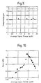
- the auto-correlation shape of the transmitted pulses does not change significantly as a function of the input power, this being clearly illustrated in Figure 9, where the ratio of the input and output correlation widths is plotted against the input power for average powers up to 3. 5 mW (120 mW peak). It should be noted that the ratio of about 0.55 varies by less than 20% over a range of power of the order of 200 x P Sa .
- the device gain follows the trend described in Figure 6, with a maximum of 17 dB occurring at an average input power of 50 ⁇ W (1.6 mW peak).
- Figures 8a and 8b A further clear demonstration of the intensity filtering properties is shown in Figures 8a and 8b.
- the amplified, shortened (to 6 ps) and pedestal-free output (Figure 8b) is shown for input pulses with substantial inter-pulse radiation ( Figure 8a). This behaviour is observed over the total range of input power.
- FIG. 2 A further embodiment of the present invention is shown in Figure 2, in which the erbium amplifier 18 of Figure 1 is now coupled to the input port 6 of the interferometer 2. Like elements are given the same reference numerals as in Figure 1.
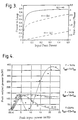
- FIG. 3 there is shown the power circulating in the two counter-propagating directions as a function of input peak power for the embodiment of Figure 1, where (a) is the power circulating anti-clockwise between the port 12 and the input of the erbium amplifier 18, and (b) is the power circulating in the loop in a clockwise direction from the erbium amplifier to the output port 12.
- the solid curve (c) of the graph of Figure 3 shows the non-linear phase shift of the pulses circulating in the two directions round the loop as a function of input peak power; and, as can be clearly seen, the non-linear phase shift becomes substantially constant at higher peak powers.
- FIG 4 there is shown a graph of the peak output power from the port 8 as a function of peak input power (in mW) of an optical signal input at the input port 6 at three different pulse repetition rates f equal to 1, 2 and 3 kHz.
- P sat equals five times the switching power, P Sa , of the interferometer of Figure 1.
- the output power is an oscillatory function of the input power. As the saturation power moves closer to the switching power with increasing frequency, the peak output power becomes more nearly a constant for peak input powers corresponding to P Sa .
- FIG. 10 there is shown a graph of the gain of the embodiment of Figure 1 as a function of the average input power of the optical signals from the optical source 24.
Landscapes
- Physics & Mathematics (AREA)
- Nonlinear Science (AREA)
- Engineering & Computer Science (AREA)
- Computer Networks & Wireless Communication (AREA)
- Signal Processing (AREA)
- Electromagnetism (AREA)
- Power Engineering (AREA)
- General Physics & Mathematics (AREA)
- Optics & Photonics (AREA)
- Optical Communication System (AREA)
- Instruments For Measurement Of Length By Optical Means (AREA)
- Spectrometry And Color Measurement (AREA)
- Lasers (AREA)
Abstract
Description
- This invention relates to an optical transmission system.
- A known optical transmission system includes an interferometer and a source of optical signals. The interferometer comprises a four port optical coupler having first and second input ports and first and second output ports, an optical coupling means coupling the first and second output ports and including an optical non-linearity, and an optical amplifier. The source of optical signals is coupled to the first input port of the interferometer.
- An optical input signal coupled to an input port of such an interferometer is split into two portions by the optical coupler, which portions counter-propagate round the coupling means, for example an optical fibre loop, to return to, and recombine at, the coupler. For a symmetric coupler, the optical path along the coupling means is the same for the two portions. So, for a 50:50 coupler and a symmetrically positioned amplifier, the portions recombine such that the input signal emerges from the port to which it was originally input. The input signal is said to be "reflected" by the interferometer. For this reason, this configuration is often described as a loop mirror, the "loop" being the optical coupling means.
- The specification of our co-pending International patent application, publication number WO 88/02875, describes an interferometer having a non-linear optical coupling means, namely a silica optical fibre loop, in which the symmetry of the two counter-propagating directions along the coupling means is broken to provide a differential non-linear effect (and so is called a non-linear optical loop mirror or NOLM). This can be achieved in various ways. For example, a non-50: 50 coupler can be used. In this case, the intensities of the signal portions coupled into the ends of the waveguide loop are not equal. When the input signal is of sufficient intensity, the signal portions propagating in opposite directions around the waveguide experience different refractive indices. This results in the two counter-propagating signal portions experiencing different phase shifts, so that, when the signals return to the coupling means, they have an intensity-dependent relative phase shift. The intensity dependence of the relative phase shift results in a device whose output at an input port is, as is well known, an oscillatory function of the intensity of the input signal. Any signal exiting the second input port (that is to say the port to which the input signal is not coupled) is said to be "transmitted" by the interferometer.
- A further way of breaking the symmetry of a NOLM is discussed in an article entitled "Nonlinear Amplifying Loop Mirror", by N E Fermann, F Haberl, M Hoffer, and H Hochreiter, Opt. Lett., 15, p.752, (1990), in which an amplifier is placed asymmetrically within the non-linear loop close to one of the output ports of the optical coupler, which in this case is a 50: 50 coupler. Such an arrangement improves the performance of the conventional NOLM, in particular by better exploitation of the waveguide loop non-linearity, as it can be accessed by a smaller input signal. The experiments described in the Fermann et al article were carried out at low signal powers, and at repetition rates which did not saturate the gain of the amplifier. It was there noted, however, that amplifier saturation leads to a reduction in the overall gain of the device although, owing to the low pulse fluences, amplifier saturation in each individual pulse could still be neglected. Such a device is called a non-linear amplifying loop mirror (NALM).
- Such NOLMs and NALMs can provide pulse shaping in optical transmission systems, and in particular provide pedestal suppression. Thus, these devices have the potential for the suppression of inter-pulse radiation, and for filtering bits in long-distance, all-optical communications systems. Such applications are discussed in an article entitled "Pulse Shaping, Compression, and Pedestal Suppression employing a Non-Linear Optical Loop Mirror" by K Smith, N J Doran, and P G J Wigley, Opt. Lett., 15, p.1294 (1990).
- A NALM could provide amplification in addition to such pulse shaping in an all-optical communications system. However, if the NALM has an oscillatory output, the intensity of the input signal must be relatively constant in order to avoid reflection by the loop mirror.
- Non-linear amplifying loop mirrors are described in papers by Richardson et al (Electronics Letters, Vol.26, No. 21, pages 1779-1781, October 1990) and Betts et al (Electronics Letters, Vol. 27, No. 10, pages 858-860, May 1991).
- The paper by Richardson is concerned with the power required to achieve switching: earlier referenced papers had switching thresholds of 100-1000W, 10-100W and, finally, a few Watts. Richardson, by using a high gain (46dB) erbium doped fibre amplifier (EDFA) reduced this to 200µw. The effect of the mark-space ratio of the input signal on the output of the EDFA was investigated - understandably, the EDFA output fell as the mark-space ratio was increased. Richardson also noted the pulse distortions produced by switching: the leading and trailing edges of square pulses are transmitted, while the centres of input pulses are reflected once the non-linear regime is entered. Richardson observed the typical oscillatory relationship between pulse input power and pulse output powers - maximum output extinction (95%) being achieved for a pulse input power of 200µw. Richardson made no mention of any influence of the EDFA on the transfer function of the NALM-except for the 200µw switching threshold.
- The paper of Betts, which cites the Richardson paper, is primarily concerned with pulse compression. The NALM included not only an EDFA but also a semiconductor laser amplifier (SLA). In this configuration the non-linear refractive index of the SLA is "used to achieve an appropriate transmission characteristic for pulse compression". The transmission characteristic which is reported, for input powers of between 20µw up to 250µw, is liner but 30 increasing. Thus, the typical oscillatory behaviour is suppressed. While the gain and the non-linear refractive index of the SLA both saturate, resulting in a desirable transmission characteristic, there is no discussion of the contribution of the EDFA and no mention or hint of saturation of the EDFA.
- The present invention provides a method of processing an optical pulse stream which comprises optical pulses, the method comprising:applying the pulse stream to a first input port of an interferometer, the interferometer comprising a four-port optical coupler which has first and second input ports and first and second output ports, an optical coupling means coupling the first and second output ports and including an optical non-linearity and an optical fibre amplifier, characterised in that the duty cycle of the optical pulse stream and the power of the optical pulses are such that the optical fibre amplifier is saturated; the interferometer is operated so that its transfer characteristic is non-oscillatory; and in that the pulse power is such that the pulses cause the interferometer to switch from a state in which its output is provided from the first input port to a state in which its output is provided from the second input port.
According to a second aspect, the invention provides an optical transmission system comprising an interferometer and a source of optical signals, the interferometer comprising a four-port optical coupler having first and second input ports and first and second output ports, an optical coupling means coupling the first and second output ports and including an optical non-linearity, the source of optical signals being coupled to the first input port of the interferometer , characterised in that the coupler is asymmetric and in that the system further comprises an optical amplifier coupled to the first input port, upstream of the output ports, to amplify the input signals prior to their being input to the interferometer, the system is such that the optical signals saturate the optical amplifier, and such that the power and duty cycle of the optical signals are such as to switch an input signal coupled to the first input port to the second input port ; the transfer function of the interferometer being non-oscillatory. - The inventive system and method achieve an approximately constant output over a range of intensities of input signal, so that a range of intensities of input optical pulse will all be switched to the output of the interferometer. Moreover, the signals will be amplified to an approximately constant intensity. The method and system, therefore, provide amplification of the signal, as well as pulse shaping and noise filtering as described in the article by Smith et al. This is of particular application to optical communications systems.
- The optical source may be a pulsed laser, in which case the optical transmission system of the present invention provides, at the second input port, noise-filtered optical pulses of substantially constant peak power, even for what may be variable peak power input pulses. The system of the invention could, therefore, be used as a repeater in a long distance optical communications link, for example a submarine link.
- The optical amplifier may comprise part of the coupling means, as described with reference to the NALMS referred to above, or may be coupled to the first input port to amplify the input signals prior to their being switched. In this latter case, the interferometer will require the symmetry to be broken by, for example, a non-50: 50 coupler as the amplifier no longer forms part of the coupling means. The interferometer may include an optical fibre loop, although other forms of waveguide may be used, for example, a waveguide formed in a planar substrate such as lithium niobate.
- In the case of an optical fibre interferometer, the optical amplifier is conveniently an optical fibre amplifier spliced to the fibre forming the loop.
- The optical fibre of the loop may be made of material exhibiting the desired non-linearity, or a separate non-linear element may be included in the loop. For example, a highly non-linear element may be incorporated to shorten the loop length, for example a semiconductor laser amplifier.
- The invention also provides a method of using an interferometer which comprises a four-port optical coupler having first and second input ports and first and second output ports, an optical coupling means coupling the first and second output ports and including an optical non-linearity, and an optical amplifier, the method comprising coupling a source of optical signals to the first input port of the interferometer in such a manner that the optical signals saturate the amplifier thereby suppressing any oscillatory output, and such that the power of the optical signals is sufficient to switch an input signal coupled to the first input port to the second input port.
- Embodiments of the present invention will now be described, by way of example, with reference to the accompanying drawings, of which:
- Figure 1 is a schematic representation of a non-linear optical loop mirror including an optical amplifier asymmetrically positioned within the waveguide loop;
- Figure 2 is a schematic representation of a non-linear optical loop mirror having an amplifier coupled to an input port;
- Figure 3 is a graph showing the power circulating in the loop for the non-linear optical mirror shown in Figure 1, and the resultant non-linear phase difference produced by various input peak powers;
- Figure 4 is a graph showing the peak output power from the embodiment of Figure 1 as a function of peak input power for three pulse repetition rates;
- Figure 5 is a graph of the non-linear phase of the embodiment of Figure 1 as a function of input peak power;
- Figure 6 is a graph showing the gain of the embodiment of Figure 1 as a function of input peak power compared to the gain provided by the amplifier of the embodiment of Figure 1 alone;
- Figure 7 is a graph showing the compression ratio provided by the embodiment of Figure 2;
- Figures 8a and 8b are reproductions of an oscillogram showing the auto-correlation traces of input pulses with substantial inter-pulse radiation and pedestal free, compressed pulses amplified by the embodiment of Figure 1, respectively;
- Figure 9 is a graph showing the auto-correlation width compression ratio as a function of input power; and
- Figure 10 is a graph showing the gain verses average input power of the embodiment of Figure 1.
-
- Referring to the drawings, Figure 1 shows an optical transmission system formed from a
Sagnac loop interferometer 2 which comprises a four-port, fused-fibreoptical coupler 4 having first andsecond input ports second output ports output ports optical fibre loop 14. Theinterferometer 2 is conveniently formed from a singleoptical fibre 14, two portions of which are fused to form thecoupler 4. In this embodiment, theloop 14 comprises an 8. 8 km length of dispersion-shifted fibre with a dispersion zero around 1. 55 µm obtained from Corning Corporation. The nature of this fibre ensures that pulse shaping due to propagation effects is negligible.Fibre polarisation controllers 16 are also included in theloop 14 to adjust the device to reflection mode at low powers. - A 30m long erbium doped fibre amplifier (EDFA) 18 is spliced to the
output port 10 of thefibre coupler 4. Anoptical fibre coupler 20 is used to couple pump radiation for theEDFA 18 from a high-powerMQW semiconductor laser 22 with a maximum pump power of the order of 50 mW at 1.48 µm. Under these conditions, theEDFA 18 has a small signal gain of 28 dB, and a time-average saturation power of 24 µW. For the above loop parameters, and an effective loop length of 7 km, the saturation power of the amplifier is of the order of 0. 6mW. - An optical source 24 (an actively mode-locked semiconductor laser providing pulses at 1.545 µm of about 12 ps duration at a repetition rate of 2.5 GHz and a mean power of about 50 µW) is connected to the
input port 6. The measured time-bandwidth products of the pulses produced by thelaser 24 are at best 0. 4. - It can be easily shown that, for the configuration of Figure 1, the square pulse transmissivity, T, is given by
amplifier 18 to break the loop symmetry provides low switching powers, together with absolute pedestal suppression for α = 0. 5. As an example, for GSS = 30 dB, α = 0.5 and L = 10 km, PSa is of the order of 0.25 mW (Aeff = 50 µm2, λ = 1.55 µm). - Considering now the effect of gain saturation of the configuration shown in Figure 1, and assuming a gain of the
form 1 + GSS/(1 + P/Psat) where GSS is the small signal gain and Psat is the input power at which the gain is compressed by 3 dB. This simple equation describes well all the measured EDFA characteristics for low to medium powers (<1 mW average), and also remains physically accurate in the highly-saturated regime. The influence of the gain saturation is best described with reference to Figure 5, where the argument of the cosine function in equation (1), that is to say the non-linear phase difference between the counter-propagating waves, is plotted against Pi, for GSS = 30 dB, psat = 0.001 (= PSa), α =0.5 and n2L/λAeff = 1. - At high input powers, the non-linear phase difference becomes clamped to πGSSPsat, which can also be expressed as πPsat/PSa since PSa, is approximately equal to 1/GSS for large GSS. Therefore, by choosing Psat = PSa we limit the maximum non-linear phase difference to π.
- The evolution of the non-linear phase is apparent in Figure 6, which shows the computed gain characteristics for sech2 intensity profile pulses (dashed curve). For comparison, the fibre amplifier gain characteristics are also shown for the same values of GSS and Psat (full curve). At low input powers, the device is in reflecting mode, and hence the small signal gain is well suppressed. As the input power is increased, however, the device approaches a transmitting state, and the efficiency closely follows that of the
EDFA 18 for Pi > PSa. It is expected that the varying response of the loop throughout the pulse gives rise to incomplete switching and pulse shaping. Although this is largely responsible for the small (2-3 dB) reduction in efficiency relative to theEDFA 18 at high powers, the loop amplifier benefits from pulse compression and low-level light suppression. - In addition, since amplifier saturation gives rise to a non-linear phase difference which, over the power range of interest, is relatively constant, the pulse shaping characteristics are fairly insensitive to the input level. This is one of the key aspects of the present invention, and is illustrated in Figure 7, where the compression ratio (τout/τin) is shown to vary only from 0.55 to 0.75 over five decades of input power. This is in stark contrast to the complex pulse shaping previously observed for loop mirror configurations, where the input power can cycle through the sinusoidal output of such prior art NOLMs. Although not obvious for the range of input power in Figure 7, τout/τin tends to unity for low power (linear) operation.
- Pulse durations are inferred from the second harmonic auto-correlation measurements. The auto-correlation shape of the transmitted pulses does not change significantly as a function of the input power, this being clearly illustrated in Figure 9, where the ratio of the input and output correlation widths is plotted against the input power for average powers up to 3. 5 mW (120 mW peak). It should be noted that the ratio of about 0.55 varies by less than 20% over a range of power of the order of 200 x PSa. The device gain follows the trend described in Figure 6, with a maximum of 17 dB occurring at an average input power of 50 µW (1.6 mW peak). The performance is well in keeping with that indicated by Figure 6, bearing in mind a 3 dB loss associated with the
loop fibre 14 and a lower (28 dB) EDFA gain. It should also be noted that the measured time-bandwidth products of the filtered pulses are essentially the same as the input. - A further clear demonstration of the intensity filtering properties is shown in Figures 8a and 8b. Here, the amplified, shortened (to 6 ps) and pedestal-free output (Figure 8b) is shown for input pulses with substantial inter-pulse radiation (Figure 8a). This behaviour is observed over the total range of input power.
- A further embodiment of the present invention is shown in Figure 2, in which the
erbium amplifier 18 of Figure 1 is now coupled to theinput port 6 of theinterferometer 2. Like elements are given the same reference numerals as in Figure 1. - In this case, the symmetry of the NOLM is broken by use of a
non-symmetric coupler 24 in place of the symmetric 50: 50coupler 4 of Figure 1, and the switching power PSb is that of the standard loop mirror (= PSa with G = 1) divided by the gain of theamplifier 18. The ratio of the switching powers of the devices of Figure 1 and Figure 2 is, therefore, given by - One can see that, for large G (which is generally true), equation (2) simplifies to PSb/PSa = (1 - α)/(1 - 2α). For a value of α = 0.4, the switching power advantage of the device of Figure 1 is at most a factor of 3. However, the real benefit of the device of Figure 1 is realised as α approaches 0.5. In this case, since the
fibre amplifier 18 breaks the loop symmetry, low switching powers are maintained, together with absolute pedestal suppression for α = 0.5. As an example, for GSS = 30 dB, α = 0.5 and L = 10 km, PSa is of the order of 0.25 mW (Aeff = 50 µm2, λ = 1.55 µm). For the device of Figure 2, however, as α approaches 0. 5 the switching power rapidly goes to infinity. - Referring now to Figure 3, there is shown the power circulating in the two counter-propagating directions as a function of input peak power for the embodiment of Figure 1, where (a) is the power circulating anti-clockwise between the
port 12 and the input of theerbium amplifier 18, and (b) is the power circulating in the loop in a clockwise direction from the erbium amplifier to theoutput port 12. The solid curve (c) of the graph of Figure 3 shows the non-linear phase shift of the pulses circulating in the two directions round the loop as a function of input peak power; and, as can be clearly seen, the non-linear phase shift becomes substantially constant at higher peak powers. - Referring now to Figure 4, there is shown a graph of the peak output power from the
port 8 as a function of peak input power (in mW) of an optical signal input at theinput port 6 at three different pulse repetition rates f equal to 1, 2 and 3 kHz. In this case, for f equal to 1 kHz, Psat equals five times the switching power, PSa, of the interferometer of Figure 1. It can be seen that the output power is an oscillatory function of the input power. As the saturation power moves closer to the switching power with increasing frequency, the peak output power becomes more nearly a constant for peak input powers corresponding to PSa. It can be seen then that, if theinterferometer 2 is operated in an optical transmission system such that amplifier saturation occurs at approximately the power necessary to switch the input power to thesecond input port 8 at the first switching peak, then approximately constant output power is achieved above the switching power. This provides pulse shaping and amplification characteristics which are relatively insensitive to the input power of the optical signals from the optical source. - Referring now to Figure 10 there is shown a graph of the gain of the embodiment of Figure 1 as a function of the average input power of the optical signals from the
optical source 24.
Claims (9)
- A method of processing an optical pulse stream which comprises optical pulses, the method comprising:
applying the optical pulses having an input power to a first input port (6) of a non-linear optical interferometer (2), the non-linear optical interferometer comprising a four-port optical coupler (4) which has first (6) and second (8) input ports and first (10) and second (12) output ports, an optical coupling means (14) coupling the first and second output ports and including an optical non-linearity and an optical fibre amplifier (18), splitting the input pulse into a first segment which travels in a first direction along the optical coupling means and a second segment which travels in the opposite second direction along the optical coupling means, whereby each of said segments is subjected to a non-linear phase shift, wherein the difference in the phase shift experienced by said first segment and said second segment varies as a function of the input power of the optical pulses, characterised by:
selecting the input peak pulse power and the repetition rate of the input pulses so as to saturate the gain of said optical fibre amplifier, so that said non-linear phase shift difference between said first and second segments is clamped to provide a non-oscillatory transfer characteristic and to cause the interferometer to switch to the state in which the processed pulses are output from the second input port. - A method according to claim 1, wherein the pulses are shaped such that the pulse shaping characteristics of said interferometer are insensitive to the input power.
- A method according to claim 1, wherein the switching power of said interferometer is equal to the saturation power of said amplifier.
- A method according to claim 1, wherein the optical coupler (4) has a power coupling coefficient, α, of between 0.4 and 0.5.
- A method as claimed in any one of claims 1 to 4, wherein the output at the second input port consists of noise-filtered optical pulses of substantially constant peak power.
- A method as claimed in any one of claims 1 to 4, wherein the optical pulse stream input to the non-linear optical interferometer includes pulses having substantial pedestals, the output from the second input port comprising optical pulses having significantly reduced pedestals.
- A method as claimed in any one of claims 1 to 4, wherein the output from the second input port comprises sech2 intensity profile pulses.
- An optical transmission system for processing an optical pulse stream which comprises optical pulses, the system comprising:
a source (24) of optical pulses, and a non-linear optical interferometer having a first input port (6), to which optical pulses from the source (24) are applied, the non-linear optical interferometer comprising a four-port optical coupler (4) which has first (6) and second (8) input ports and first (10) and second (12) output ports, an optical coupling means (14) coupling the first and second output ports and including an optical non-linearity and an optical fibre amplifier (18), wherein said optical coupler (4) splits the input pulse into a first segment which travels in a first direction along the optical coupling means (14) and a second segment which travels in the opposite second direction along the optical coupling means (14), wherein each of said segments is subjected to a non-linear phase shift, wherein the difference in the phase shift experienced by said first segment and said second segment varies as a function of the input power of the optical pulses, characterised in that:
the optical transmission system is configured so that said source (24) provides pulses having a peak pulse power and a repetition rate such as to saturate the gain of said optical fibre amplifier, whereby said non-linear phase shift difference between said first and second segments is clamped to provide a non-oscillatory transfer characteristic and to cause the interferometer to switch to the state in which the processed pulses are output from the second input port. - An optical communications link including
a source (24) of optical pulses, an optical fibre transmission path and a repeater within the transmission path, the repeater including a non-linear optical interferometer (2) including a four-port optical coupler (4) which has first (6) and second (8) input ports and first (10) and second (12) output ports, an optical coupling means (14) coupling the first and second output ports and including an optical non-linearity and an optical fibre amplifier (18), optical pulses from the source (24) passing along the transmission path to the first input port (6) of the interferometer, wherein said optical coupler (4) splits the input pulse into a first segment which travels in a first direction along the optical coupling means (14) and a second segment which travels in the opposite second direction along the optical coupling means (14), wherein each of said segments is subjected to a non-linear phase shift, wherein the difference in the phase shift experienced by said first segment and said second segment varies as a function of the input power of the optical pulses, characterised in that:
the optical communications link is configured so that said source (24) provides pulses having an input peak pulse power and a repetition rate such as to saturate the gain of said optical fibre amplifier, whereby said non-linear phase shift difference between said first and second segments is clamped to provide a non-oscillatory transfer characteristic and to cause the interferometer to switch to the state in which the processed pulses are output from the second input port.
Applications Claiming Priority (3)
| Application Number | Priority Date | Filing Date | Title |
|---|---|---|---|
| GB9118843 | 1991-09-03 | ||
| GB919118843A GB9118843D0 (en) | 1991-09-03 | 1991-09-03 | An optical transmission system |
| PCT/GB1992/001579 WO1993005592A1 (en) | 1991-09-03 | 1992-08-28 | Non-linear optical interferometer with saturated amplifier |
Publications (2)
| Publication Number | Publication Date |
|---|---|
| EP0602089A1 EP0602089A1 (en) | 1994-06-22 |
| EP0602089B1 true EP0602089B1 (en) | 2001-04-04 |
Family
ID=10700847
Family Applications (1)
| Application Number | Title | Priority Date | Filing Date |
|---|---|---|---|
| EP92918236A Expired - Lifetime EP0602089B1 (en) | 1991-09-03 | 1992-08-28 | Non-linear optical interferometer with saturated amplifier |
Country Status (12)
| Country | Link |
|---|---|
| US (1) | US5479291A (en) |
| EP (1) | EP0602089B1 (en) |
| JP (1) | JPH06510135A (en) |
| KR (1) | KR100272402B1 (en) |
| AT (1) | ATE200368T1 (en) |
| AU (1) | AU656225B2 (en) |
| CA (1) | CA2112596C (en) |
| DE (1) | DE69231767T2 (en) |
| ES (1) | ES2157206T3 (en) |
| GB (2) | GB9118843D0 (en) |
| HK (1) | HK154696A (en) |
| WO (1) | WO1993005592A1 (en) |
Families Citing this family (28)
| Publication number | Priority date | Publication date | Assignee | Title |
|---|---|---|---|---|
| GB9122182D0 (en) * | 1991-10-18 | 1991-11-27 | British Telecomm | Optical memory |
| EP0567693A1 (en) * | 1992-04-27 | 1993-11-03 | BRITISH TELECOMMUNICATIONS public limited company | Optical clock recovery |
| US5825530A (en) * | 1994-12-02 | 1998-10-20 | Hewlett-Packard Company | Arrangement and method for operating and testing an optical device |
| CA2207504C (en) * | 1994-12-23 | 2001-07-31 | British Telecommunications Public Limited Company | Node in optical tdm network |
| JP3272895B2 (en) * | 1995-02-24 | 2002-04-08 | 安藤電気株式会社 | Optical pulse generator |
| WO1996031023A1 (en) * | 1995-03-24 | 1996-10-03 | British Telecommunications Public Limited Company | Optical network |
| EP0753787A1 (en) * | 1995-07-05 | 1997-01-15 | Koninklijke Philips Electronics N.V. | Optical unit for processing an optical pulse pattern |
| US6157762A (en) * | 1996-12-09 | 2000-12-05 | The Regents Of The University Of California | Nonlinear pulse reshaping for optical fiber transmission systems |
| US6052393A (en) | 1996-12-23 | 2000-04-18 | The Regents Of The University Of Michigan | Broadband Sagnac Raman amplifiers and cascade lasers |
| WO1999041855A2 (en) * | 1998-02-16 | 1999-08-19 | Koninklijke Philips Electronics N.V. | Optical transmission system with a receiver using full optical clock recovery |
| US6374006B1 (en) | 1998-03-20 | 2002-04-16 | Xtera Communications, Inc. | Chirped period gratings for raman amplification in circulator loop cavities |
| US6600592B2 (en) | 1998-03-24 | 2003-07-29 | Xtera Communications, Inc. | S+ band nonlinear polarization amplifiers |
| US6760148B2 (en) | 1998-03-24 | 2004-07-06 | Xtera Communications, Inc. | Nonlinear polarization amplifiers in nonzero dispersion shifted fiber |
| US6356384B1 (en) * | 1998-03-24 | 2002-03-12 | Xtera Communications Inc. | Broadband amplifier and communication system |
| US6335820B1 (en) | 1999-12-23 | 2002-01-01 | Xtera Communications, Inc. | Multi-stage optical amplifier and broadband communication system |
| US6574037B2 (en) | 1998-06-16 | 2003-06-03 | Xtera Communications, Inc. | All band amplifier |
| US6885498B2 (en) | 1998-06-16 | 2005-04-26 | Xtera Communications, Inc. | Multi-stage optical amplifier and broadband communication system |
| US6359725B1 (en) | 1998-06-16 | 2002-03-19 | Xtera Communications, Inc. | Multi-stage optical amplifier and broadband communication system |
| WO1999066607A2 (en) | 1998-06-16 | 1999-12-23 | Xtera Communications, Inc. | Fiber-optic compensation for dispersion, gain tilt, and band pump nonlinearity |
| US6567430B1 (en) | 1998-09-21 | 2003-05-20 | Xtera Communications, Inc. | Raman oscillator including an intracavity filter and amplifiers utilizing same |
| SE516882C2 (en) * | 1998-12-23 | 2002-03-19 | Ericsson Telefon Ab L M | Device for reflecting light |
| US6295308B1 (en) * | 1999-08-31 | 2001-09-25 | Corning Incorporated | Wavelength-locked external cavity lasers with an integrated modulator |
| WO2001052372A1 (en) | 2000-01-12 | 2001-07-19 | Xtera Communications, Inc. | Raman amplifier with bi-directional pumping |
| WO2001078264A2 (en) | 2000-02-14 | 2001-10-18 | Xtera Communications, Inc. | Nonlinear optical loop mirror |
| US6404541B2 (en) * | 2000-03-24 | 2002-06-11 | Oprel Technologies Inc. | Optical amplifier with active-fiber loop mirror |
| US6744553B1 (en) | 2000-06-20 | 2004-06-01 | Xtera Communications, Inc. | System and method for converting a plurality of wavelengths |
| ITMI20031773A1 (en) * | 2003-09-17 | 2005-03-18 | Marconi Comm Spa | OPTICAL SIGNAL REGENERATOR FOR TRANSMISSION SYSTEMS WITH HIGH BIT RATES |
| JP2005173530A (en) * | 2003-11-17 | 2005-06-30 | Osaka Industrial Promotion Organization | Light signal processing method and device, nonlinear optical loop mirror and its design method, and light signal conversion method |
Family Cites Families (2)
| Publication number | Priority date | Publication date | Assignee | Title |
|---|---|---|---|---|
| US5369520A (en) * | 1992-05-22 | 1994-11-29 | At&T Corp. | Optical regeneration circuit |
| US5309267A (en) * | 1992-09-25 | 1994-05-03 | At&T Bell Laboratories | Optical communication system using a Sagnac switch |
-
1991
- 1991-09-03 GB GB919118843A patent/GB9118843D0/en active Pending
-
1992
- 1992-08-28 KR KR1019940700509A patent/KR100272402B1/en not_active IP Right Cessation
- 1992-08-28 GB GB9325690A patent/GB2274036B/en not_active Expired - Fee Related
- 1992-08-28 US US08/199,299 patent/US5479291A/en not_active Expired - Lifetime
- 1992-08-28 DE DE69231767T patent/DE69231767T2/en not_active Expired - Lifetime
- 1992-08-28 WO PCT/GB1992/001579 patent/WO1993005592A1/en active IP Right Grant
- 1992-08-28 JP JP5505027A patent/JPH06510135A/en active Pending
- 1992-08-28 EP EP92918236A patent/EP0602089B1/en not_active Expired - Lifetime
- 1992-08-28 AU AU24923/92A patent/AU656225B2/en not_active Ceased
- 1992-08-28 AT AT92918236T patent/ATE200368T1/en not_active IP Right Cessation
- 1992-08-28 CA CA002112596A patent/CA2112596C/en not_active Expired - Fee Related
- 1992-08-28 ES ES92918236T patent/ES2157206T3/en not_active Expired - Lifetime
-
1996
- 1996-08-15 HK HK154696A patent/HK154696A/en not_active IP Right Cessation
Also Published As
| Publication number | Publication date |
|---|---|
| WO1993005592A1 (en) | 1993-03-18 |
| DE69231767D1 (en) | 2001-05-10 |
| US5479291A (en) | 1995-12-26 |
| AU2492392A (en) | 1993-04-05 |
| JPH06510135A (en) | 1994-11-10 |
| DE69231767T2 (en) | 2001-10-25 |
| GB2274036B (en) | 1995-07-05 |
| CA2112596C (en) | 1998-01-20 |
| GB9118843D0 (en) | 1991-10-16 |
| ATE200368T1 (en) | 2001-04-15 |
| KR100272402B1 (en) | 2000-11-15 |
| HK154696A (en) | 1996-08-23 |
| CA2112596A1 (en) | 1993-03-18 |
| EP0602089A1 (en) | 1994-06-22 |
| GB2274036A (en) | 1994-07-06 |
| AU656225B2 (en) | 1995-01-27 |
| ES2157206T3 (en) | 2001-08-16 |
| GB9325690D0 (en) | 1994-03-09 |
Similar Documents
| Publication | Publication Date | Title |
|---|---|---|
| EP0602089B1 (en) | Non-linear optical interferometer with saturated amplifier | |
| Agrawal | Nonlinear fiber optics | |
| US5757529A (en) | In-line regenerating apparatus for regenerating a soliton-conveyed signal by synchronously modulating the solitons by means of a non-linear optical loop mirror | |
| EP1130456B1 (en) | Method, device, and system for waveform shaping of signal light | |
| US6453082B1 (en) | Device and system for waveform shaping | |
| EP1430574A2 (en) | Optical fibre-based devices utilising the raman effect | |
| AU615363B2 (en) | Non-linear interferometer | |
| Deshmukh et al. | Four wave mixing in DWDM optical system | |
| Olsson et al. | Polarization independent demultiplexing in a polarization diversity nonlinear optical loop mirror | |
| Dahir et al. | Dispersion compensation by using FBG and low pass Gaussian filter | |
| Maruta et al. | Effectiveness of densely dispersion managed solitons in ultra-high speed transmission | |
| Wu et al. | Optimization of pulse compression with an unbalanced nonlinear optical loop mirror | |
| Toda et al. | Optical soliton transmission experiment in a comb-like dispersion profiled fiber loop | |
| Chi et al. | 2R regenerator based on high non-linear dispersion-imbalanced loop mirror | |
| EP0850515A2 (en) | Optical pulse propagation | |
| Veith | Useful and detrimental aspects of self-phase modulation in fiber optical applications | |
| Erro et al. | Third-order dispersion in linearly chirped Bragg gratings and its compensation | |
| Man et al. | Optimal loop length of a nonlinear optical loop mirror in switching solitons | |
| Tomlinson | Nonlinear Phenomena in Single‐Mode Optical Fibers | |
| White et al. | Towards Ultimate Pulse Propagation in Optical Fibres | |
| Flores-Rosas et al. | Stimulated Raman Scattering for All Optical Switches | |
| Lee et al. | All optical RZ to NRZ format conversion using phase modulation in a dispersion-shifted fiber | |
| Evans | Dispersion-tapered fiber in nonlinear loop mirrors for intensity and pulse width switching | |
| Hasegawa et al. | Other Applications of Optical Solitons | |
| Fok et al. | Bismuth-oxide highly nonlinear fiber based dispersion imbalanced loop mirror for RZ signal regeneration |
Legal Events
| Date | Code | Title | Description |
|---|---|---|---|
| PUAI | Public reference made under article 153(3) epc to a published international application that has entered the european phase |
Free format text: ORIGINAL CODE: 0009012 |
|
| 17P | Request for examination filed |
Effective date: 19931220 |
|
| AK | Designated contracting states |
Kind code of ref document: A1 Designated state(s): AT BE CH DE DK ES FR IT LI LU NL SE |
|
| 17Q | First examination report despatched |
Effective date: 19961223 |
|
| REG | Reference to a national code |
Ref country code: GB Ref legal event code: 732E |
|
| GRAG | Despatch of communication of intention to grant |
Free format text: ORIGINAL CODE: EPIDOS AGRA |
|
| GRAG | Despatch of communication of intention to grant |
Free format text: ORIGINAL CODE: EPIDOS AGRA |
|
| GRAH | Despatch of communication of intention to grant a patent |
Free format text: ORIGINAL CODE: EPIDOS IGRA |
|
| RBV | Designated contracting states (corrected) |
Designated state(s): AT BE CH DE DK ES FR IT LI LU NL SE |
|
| GRAH | Despatch of communication of intention to grant a patent |
Free format text: ORIGINAL CODE: EPIDOS IGRA |
|
| GRAA | (expected) grant |
Free format text: ORIGINAL CODE: 0009210 |
|
| AK | Designated contracting states |
Kind code of ref document: B1 Designated state(s): AT BE CH DE DK ES FR IT LI LU NL SE |
|
| PG25 | Lapsed in a contracting state [announced via postgrant information from national office to epo] |
Ref country code: NL Free format text: LAPSE BECAUSE OF FAILURE TO SUBMIT A TRANSLATION OF THE DESCRIPTION OR TO PAY THE FEE WITHIN THE PRESCRIBED TIME-LIMIT Effective date: 20010404 Ref country code: LI Free format text: LAPSE BECAUSE OF FAILURE TO SUBMIT A TRANSLATION OF THE DESCRIPTION OR TO PAY THE FEE WITHIN THE PRESCRIBED TIME-LIMIT Effective date: 20010404 Ref country code: CH Free format text: LAPSE BECAUSE OF FAILURE TO SUBMIT A TRANSLATION OF THE DESCRIPTION OR TO PAY THE FEE WITHIN THE PRESCRIBED TIME-LIMIT Effective date: 20010404 Ref country code: BE Free format text: LAPSE BECAUSE OF FAILURE TO SUBMIT A TRANSLATION OF THE DESCRIPTION OR TO PAY THE FEE WITHIN THE PRESCRIBED TIME-LIMIT Effective date: 20010404 Ref country code: AT Free format text: LAPSE BECAUSE OF FAILURE TO SUBMIT A TRANSLATION OF THE DESCRIPTION OR TO PAY THE FEE WITHIN THE PRESCRIBED TIME-LIMIT Effective date: 20010404 |
|
| REF | Corresponds to: |
Ref document number: 200368 Country of ref document: AT Date of ref document: 20010415 Kind code of ref document: T |
|
| REG | Reference to a national code |
Ref country code: CH Ref legal event code: EP |
|
| REF | Corresponds to: |
Ref document number: 69231767 Country of ref document: DE Date of ref document: 20010510 |
|
| ITF | It: translation for a ep patent filed | ||
| PG25 | Lapsed in a contracting state [announced via postgrant information from national office to epo] |
Ref country code: SE Free format text: LAPSE BECAUSE OF FAILURE TO SUBMIT A TRANSLATION OF THE DESCRIPTION OR TO PAY THE FEE WITHIN THE PRESCRIBED TIME-LIMIT Effective date: 20010704 |
|
| ET | Fr: translation filed | ||
| REG | Reference to a national code |
Ref country code: ES Ref legal event code: FG2A Ref document number: 2157206 Country of ref document: ES Kind code of ref document: T3 |
|
| PG25 | Lapsed in a contracting state [announced via postgrant information from national office to epo] |
Ref country code: LU Free format text: LAPSE BECAUSE OF NON-PAYMENT OF DUE FEES Effective date: 20010828 |
|
| NLV1 | Nl: lapsed or annulled due to failure to fulfill the requirements of art. 29p and 29m of the patents act | ||
| PG25 | Lapsed in a contracting state [announced via postgrant information from national office to epo] |
Ref country code: DK Free format text: LAPSE BECAUSE OF FAILURE TO SUBMIT A TRANSLATION OF THE DESCRIPTION OR TO PAY THE FEE WITHIN THE PRESCRIBED TIME-LIMIT Effective date: 20011011 |
|
| REG | Reference to a national code |
Ref country code: CH Ref legal event code: PL |
|
| PLBE | No opposition filed within time limit |
Free format text: ORIGINAL CODE: 0009261 |
|
| STAA | Information on the status of an ep patent application or granted ep patent |
Free format text: STATUS: NO OPPOSITION FILED WITHIN TIME LIMIT |
|
| 26N | No opposition filed | ||
| PGFP | Annual fee paid to national office [announced via postgrant information from national office to epo] |
Ref country code: IT Payment date: 20060831 Year of fee payment: 15 |
|
| REG | Reference to a national code |
Ref country code: FR Ref legal event code: TP |
|
| PG25 | Lapsed in a contracting state [announced via postgrant information from national office to epo] |
Ref country code: IT Free format text: LAPSE BECAUSE OF NON-PAYMENT OF DUE FEES Effective date: 20070828 |
|
| PGFP | Annual fee paid to national office [announced via postgrant information from national office to epo] |
Ref country code: ES Payment date: 20090821 Year of fee payment: 18 |
|
| PGFP | Annual fee paid to national office [announced via postgrant information from national office to epo] |
Ref country code: DE Payment date: 20090821 Year of fee payment: 18 |
|
| REG | Reference to a national code |
Ref country code: FR Ref legal event code: ST Effective date: 20110502 |
|
| REG | Reference to a national code |
Ref country code: DE Ref legal event code: R119 Ref document number: 69231767 Country of ref document: DE Effective date: 20110301 |
|
| PG25 | Lapsed in a contracting state [announced via postgrant information from national office to epo] |
Ref country code: FR Free format text: LAPSE BECAUSE OF NON-PAYMENT OF DUE FEES Effective date: 20100831 Ref country code: DE Free format text: LAPSE BECAUSE OF NON-PAYMENT OF DUE FEES Effective date: 20110301 |
|
| PGFP | Annual fee paid to national office [announced via postgrant information from national office to epo] |
Ref country code: FR Payment date: 20090914 Year of fee payment: 18 |
|
| REG | Reference to a national code |
Ref country code: ES Ref legal event code: FD2A Effective date: 20111118 |
|
| PG25 | Lapsed in a contracting state [announced via postgrant information from national office to epo] |
Ref country code: ES Free format text: LAPSE BECAUSE OF NON-PAYMENT OF DUE FEES Effective date: 20100829 |