EP0601580B1 - Apparatus and method for measuring the thickness of thin films - Google Patents
Apparatus and method for measuring the thickness of thin films Download PDFInfo
- Publication number
- EP0601580B1 EP0601580B1 EP93119876A EP93119876A EP0601580B1 EP 0601580 B1 EP0601580 B1 EP 0601580B1 EP 93119876 A EP93119876 A EP 93119876A EP 93119876 A EP93119876 A EP 93119876A EP 0601580 B1 EP0601580 B1 EP 0601580B1
- Authority
- EP
- European Patent Office
- Prior art keywords
- self
- thickness
- layer
- normalized
- wavelengths
- Prior art date
- Legal status (The legal status is an assumption and is not a legal conclusion. Google has not performed a legal analysis and makes no representation as to the accuracy of the status listed.)
- Expired - Lifetime
Links
Images


Classifications
-
- H—ELECTRICITY
- H10—SEMICONDUCTOR DEVICES; ELECTRIC SOLID-STATE DEVICES NOT OTHERWISE PROVIDED FOR
- H10P—GENERIC PROCESSES OR APPARATUS FOR THE MANUFACTURE OR TREATMENT OF DEVICES COVERED BY CLASS H10
- H10P74/00—Testing or measuring during manufacture or treatment of wafers, substrates or devices
- H10P74/20—Testing or measuring during manufacture or treatment of wafers, substrates or devices characterised by the properties tested or measured, e.g. structural or electrical properties
- H10P74/203—Structural properties, e.g. testing or measuring thicknesses, line widths, warpage, bond strengths or physical defects
-
- G—PHYSICS
- G01—MEASURING; TESTING
- G01B—MEASURING LENGTH, THICKNESS OR SIMILAR LINEAR DIMENSIONS; MEASURING ANGLES; MEASURING AREAS; MEASURING IRREGULARITIES OF SURFACES OR CONTOURS
- G01B11/00—Measuring arrangements characterised by the use of optical techniques
- G01B11/02—Measuring arrangements characterised by the use of optical techniques for measuring length, width or thickness
- G01B11/06—Measuring arrangements characterised by the use of optical techniques for measuring length, width or thickness for measuring thickness ; e.g. of sheet material
- G01B11/0616—Measuring arrangements characterised by the use of optical techniques for measuring length, width or thickness for measuring thickness ; e.g. of sheet material of coating
- G01B11/0625—Measuring arrangements characterised by the use of optical techniques for measuring length, width or thickness for measuring thickness ; e.g. of sheet material of coating with measurement of absorption or reflection
-
- H—ELECTRICITY
- H10—SEMICONDUCTOR DEVICES; ELECTRIC SOLID-STATE DEVICES NOT OTHERWISE PROVIDED FOR
- H10P—GENERIC PROCESSES OR APPARATUS FOR THE MANUFACTURE OR TREATMENT OF DEVICES COVERED BY CLASS H10
- H10P74/00—Testing or measuring during manufacture or treatment of wafers, substrates or devices
- H10P74/27—Structural arrangements therefor
Definitions
- the present invention relates to an apparatus and method for measuring a thin film or layer thickness and, without limitation, to an electro-optical system which measures the thickness of an outer silicon layer of a silicon/silicon dioxide/silicon (Si/SiO 2 /Si) structured semiconductor wafer.
- a silicon-on-insulator (SOI) semiconductor wafer which typically includes a Si/SiO 2 /Si sandwich structure fabricated by growing a silicon dioxide film on one surface of each of two silicon wafers and bonding the two silicon dioxide film surfaces together at high temperature.
- SOI silicon-on-insulator
- the earlier invention and the present invention can be used for measuring any number of layers providing only one layer thickness is unknown and the optical properties of all layers are accurately known.
- other materials such as, for example, silicon nitride, may be used for the insulator material and that other materials may be used for the wafer material.
- one of the two outer silicon surfaces of the sandwich structure is mechanically ground and polished to an average thickness of several microns.
- This mechanical process unfortunately results in large spatial variations in the thickness of this outer silicon layer over the surface of the wafer.
- a thickness error map that indicates thickness non-uniformities of this outer silicon layer over the entire wafer surface, is required, for example, to initialize a further micropolishing process.
- a measurement of at least 400 points on a wafer surface in 60 seconds is desirable.
- measuring instruments typically provided film thickness measurements at only a single point on a surface. These instruments use a focused lens or a fiber bundle to locally illuminate the film surface with a beam of monochromatic light, and a grating or prism spectrograph to measure the surface spectral reflectance at each point. In all cases, this surface spectral reflectance data must be numerically corrected due to variations in the angle of incidence caused by the illuminating beam f-number.
- the above cited application disclosed an electro-optical imaging system for efficiently determining a thin film layer thickness of, for example, a wafer over a full aperture.
- Non-uniformities in this layer thickness are obtained by measuring the reflectance characteristics for a full aperture of a wafer surface and comparing this measured reflectance data to reference reflectance data by using numerical iteration or by using a calibration wafer having known layer thicknesses.
- a filtered white light source is used to produce a sequence of collimated monochromatic light beams at several different wavelengths. These collimated monochromatic beams are individually projected onto the entire surface of the wafer, and coherent interactions occur between this light as it is reflected from the physical boundaries in the wafer structure. As a result of these interactions an interference fringe pattern is formed on the surface of the wafer for each projected beam and, consequently, for each wavelength. A reflected image of each fringe pattern is projected onto a detector array of, for example, a charge coupled device (CCD) camera, where the full aperture of this image is then captured.
- CCD charge coupled device
- the fringe pattern image is captured by digitizing pixels in the CCD camera detector array corresponding to the image present.
- a reflectance map of the entire wafer surface is generated from this captured fringe pattern image.
- Several reflectance maps are generated from each measured wafer to eliminate thickness ambiguities which may result from outer layers having phase thicknesses greater than 2 ⁇ .
- the reference reflectance data for a wafer may be obtained, according to the above cited application, by a theoretical calculation or through the use of a calibration wafer.
- the theoretical method consists of numerically computing reference reflectance characteristics based on assumed values for the intrinsic optical properties of the wafer materials.
- a calibration wafer, having a known thickness profile may be constructed from the same batch of materials used to construct the wafer to be measured. By subjecting this calibration wafer to the measuring method of the present invention, reference reflectance data is obtained for the known wafer.
- the comparison between the measured reflectance data and the reference reflectance data can then be performed by a computer.
- the computer can provide a mapping of layer thickness or a mapping of layer thickness non-uniformities over a full aperture of the wafer.
- the silicon-on-insulator (SOI) wafers that are measured consist of two silicon wafers sandwiching a thin layer of silicon dioxide and typically suffer mechanical distortion caused by the manufacturing and polishing process. This results in surface deformations of 50 to 100 microns and local slope changes up to 1/4 a degree.
- measurement of the thickness of the outer film of silicon requires forming images of the wafer on a CCD camera at various monochromatic wavelengths in the visible region. The images are digitized (512 x 512 pixels) and this data is used to derive the spatial variations of the wafer reflectance caused by differing thicknesses of the silicon film.
- a library of reflectance values for different values of the outer film thickness is precalculated at all the different wavelengths and is used to find a match between the measured sampled spectral reflectance and the precalculated sampled spectrum by using a least squares fitting technique.
- This calculation requires the actual reflectances of the SOI wafer to be derived from the digitized data before the least squares fitting technique can be carried out.
- the intensities in the digitized images are not only proportional to the wafer reflectances but also to the spectral properties of the light source, the camera and the coatings in the optical system.
- an absolute measure of the SOI wafer reflectance can be obtained by recording an additional set of images of a bare silicon wafer, and since the reflectance of bare silicon is accurately known, then the wafer reflectance can be scaled from the data in the two sets of images.
- the use of two sets of measurements at different times requires that the two wafers being accurately aligned in position and angle.
- the light source must also be stable in amplitude over the measurement time of about one minute.
- An object of the present invention is to improve the above thickness determination by reducing the necessary memory capacity.
- each pixel can be treated as an independent reflectometer and that each reflection at a given wavelength for that pixel can be self-normalized with respect to other reflections at different wavelengths for the same pixel.
- uniformity variations in reflectance caused by spectral response can be premeasured and eliminated in advance of calculating the merit function.
- the use of wafer reflectance in the merit function can be replaced by matching a self normalized reflectance pattern as opposed to an absolute reflectance pattern.
- This new approach allows the number of measured images to be reduced by a factor of two by eliminating the need for measurements on a bare silicon wafer.
- the 2N measurements are replaced by N images and N spectral shape calibration constants.
- Measured data from one pixel consists of N digitized values V 1 ...V N at the wavelengths ⁇ 1 ... ⁇ N and the data at a pixel is normalized by dividing the data V k at a given wavelength by the sum of all the digitized values at all the wavelengths.
- These ratios can also be further modified to create a flat spectral response by dividing each one by the gain of the system. Since the library also has a flat spectral response, the ratios can also be computed theoretically and used in the least squares pattern matching technique.
- Figure 1 is a schematic representation of a wafer layer thickness measuring instrument that can be used according to the present invention.
- Figure 2 is a cross-sectional view of a SOI semiconductor wafer.
- Figure 3 is a plan view of a CCD camera detector array showing a wafer image outline and several reference surface image outlines.
- Figure 4 is a flow chart showing a self-normalized method according to the present invention.
- FIG. 1 An electro-optical system for measuring a layer thickness of a wafer 24 , according to the present invention, is shown in Figure 1. For the purposes of this description, the measurement of an outer silicon layer of a SOI semiconductor wafer 24 is described.
- the apparatus of Fig. 1 provides a white light source comprised of a circular aperture 14 illuminated by a halogen lamp 10 and a condensing lens 12 .
- a white light source comprised of a circular aperture 14 illuminated by a halogen lamp 10 and a condensing lens 12 .
- Light passing through aperture 14 impinges on a collimator lens 16 to form a beam 15 of collimated light.
- the size of the aperture 14 determines the field angles in the collimated light sections of the optical system and the orientation is chosen to allow an aperture image to be projected onto the SOI wafer 24 .
- the condensing lens 12 may be replaced by a fiber optic light guide.
- the white light source is spectrally filtered by a series of narrow band filters 17 , nominally of 30 to 50 ⁇ half bandwidth, placed in the collimated beam 15 .
- the series of filters 17 are placed around the periphery of a rotating filter wheel assembly 18 , whereby a corresponding series of collimated monochromatic light beams 19 are produced.
- the wavelengths of these collimated monochromatic light beams 19 range, for example, from 550nm to 950nm. Locating the filter wheel assembly 18 in a collimated light section 15 minimizes the spectral broadening of the filtered beam 19 caused by the field angle defined by the size of the aperture 14 .
- a pair of electronic signals 32 are generated by the filter wheel assembly 18 to serve as a timing reference 33 for a digitizing circuit 34 . One of these signals indicates the beginning of a filter wheel revolution, whereas the other signal indicates the beginning of each filter period.
- a second collimator lens 20 forms a monochromatic image of the aperture 14 about a point 21 in a focal plane of a third collimator lens 22 .
- This third collimator lens 22 produces a collimated beam 23 which illuminates the full aperture of, for example, a 100 millimeter diameter SOI wafer 24 .
- an extension of this wafer illumination technique to wafers of 150 millimeters or 200 millimeters in diameter requires that the size of the third collimator lens 22 match the wafer size.
- a monochromator can replace the halogen lamp 10 , the condensing lens 12 , the first two collimator lenses 16 , 20 , and the narrow band filter wheel 18 , provided that the slewing rate of the monochromator between different wavelengths is sufficiently high, up to twenty different wavelengths in less than one second.
- FIG. 2 an exaggerated cross-sectional view of a SOI semiconductor wafer 24 is shown.
- This wafer 24 is constructed in a sandwich structure consisting of a mechanically polished outer silicon layer 40 , an internal silicon dioxide (SiO 2 ) film 42 , and a silicon wafer substrate 44 .
- This sandwich structure creates three interfaces 46 , 48 , 50 from which light, incident upon the outer silicon layer 40 , may be reflected.
- the reflectance characteristics of these interfaces 46 , 48 , 50 are based upon the intrinsic optical and physical properties of the semiconductor materials in each layer 40 , 42 , 44 of the SOI wafer 24 .
- the wafer reflectance at any wavelength can be calculated explicitly as a function of the outer film thickness if all the other parameters are known; however, the reverse problem of computing the thickness from a single measured reflectance is ambiguous. This ambiguity is created by the fact that as the outer film thickness is increased, the measured reflectance cycles between maximum and minimum values as the phase thickness (n 2 t 2 ) increases by multiples of ⁇ /4. This multi-valued problem clearly makes the computation of the value of t 2 from a single reflectance measurement impossible.
- the use of multiple wavelength measurements can in principle overcome the multiple value problem but the wavelength dependent behavior of the material properties must be very accurately known; otherwise, large errors occur in the thickness computations.
- An alternate approach is a statistical one where measured reflectance data at several wavelengths is compared on a least squares best fit basis with a library of computed spectral data at the same wavelengths.
- the library of spectra is computed for all values of the outer film thickness and the selection is made by choosing that outer film thickness which minimizes the least squares fit.
- a collimated light image of the interference fringe pattern is reflected off the surface of the SOI wafer 24 and returned through the third collimator lens 22 .
- This third collimator lens 22 projects a condensed image of the reflected fringe pattern upon an off-axis mirror 26 .
- This mirror 26 is positioned at a point 25 in the focal plane of the third collimator lens 22 , alongside the position of the aperture image at focal point 21 .
- the separation of these two focal points 21 , 25 may be controlled with a slight lateral shift in the optical axis of the third collimator lens 22 with respect to the optical axis of the condensing lens 12 and the first two collimator lenses 16 , 20 .
- the wafer 24 may be tilted through a small angle, less than one degree, to achieve this same effect.
- This image separation scheme avoids the use of a beamsplitter which contains metallic coatings with attendant optical losses.
- the off-axis mirror 26 is used to redirect the reflected fringe pattern image from the wafer 24 to a final collimator lens 28 .
- This final collimator lens 28 projects a collimated beam 29 containing an image of the fringe pattern onto a CCD camera detector array 31 .
- the filter wheel assembly 18 may also be placed in this collimated beam 29 provided that the field angle, which is approximately fifteen times larger than the field angle in the collimated beam 23 illuminating the wafer 24 , can be tolerated by the narrow band filters.
- An alternate method of providing the reflected fringe pattern image to the CCD camera detector array 31 is shown in a dashed line block 61 in Figure 1 .
- An on-axis beamsplitter 60 is placed in the collimated light beam section 19 where the filter wheel assembly 18 is positioned.
- the beamsplitter 60 receives a collimated fringe pattern image from the second collimator lens 20 and reflects a portion 62 of this collimated beam to a final collimator lens 64 .
- This final collimator lens 64 converges the fringe pattern image onto the CCD camera detector array 31 .
- the filter wheel assembly 18 may be placed in the collimated beam 62 reflected by the beamsplitter 60 , provided that the field angle can be tolerated by the narrow band filters 17 .
- the determination of the method used to provide the reflected fringe pattern image to the CCD camera 30 is critically dependent upon the optical performance of the third collimator lens 22 .
- the optical design of the third collimator lens 22 must possess an optimal off-axis performance quality and provide a minimal radial color distortion effect.
- Optimal off-axis performance minimizes the distortion effects associated with field angles that are created when the collimated light beam 23 is reflected from an off-axis non-uniform surface of a SOI wafer 24 .
- the need for a consistent fringe pattern image size at the CCD camera detector array 31 requires radial color distortion correction over the wavelength region of the incident monochromatic light.
- the on-axis beamsplitter method When the on-axis beamsplitter method is used, however, only the radial color distortion correction requirement applies since the field angles produced in the collimated light beam 23 reflected from an on-axis SOI wafer surface 46 are negligible. Therefore, if the returned fringe pattern image is distorted due to sub-optimal off-axis performance by the third collimator lens 22 , then the off-axis mirror method is unsuitable and an on-axis beamsplitter 60 must be used.
- the CCD camera detector array 31 is shown with an image of a scaled SOI wafer outline 52 , a pair of reference alignment images 54 , and a pair of reference reflecting images 56 , projected upon its surface.
- These reference images are formed by placing reference alignment marks and reference reflecting surfaces along the same plane as the surface of the SOI wafer 24 .
- these references provide reflections from their surfaces.
- images of these reflected references are returned through the third collimator lens 22 and are eventually projected upon the CCD camera detector array 31 .
- the reference alignment marks provide aid in wafer alignment, whereas the reference reflecting surfaces are used to self-normalize the CCD signals, according to the invention, so that actual wafer reflectances can be calculated.
- the collimated beam 29 formed by the final collimator lens 28 contains an image of the reflected fringe pattern.
- This image is projected upon the CCD camera detector array 31 and captured by the CCD camera 30 .
- a reflectance map is generated by digitizing the CCD pixel signals corresponding to the projected fringe pattern image with a digitizing circuit 34 .
- This raw reflectance data may be normalized to eliminate variations in pixel sensitivity and may be reduced in size by averaging signals over blocks of pixels to match the spatial limitations of the subsequent chemical micropolishing process.
- a numerical computation method is used in determining the thickness, t 2 of the outer silicon layer of the SOI wafer 24 . Both of these methods require the use of a computer 36 .
- the numerical method of determining outer silicon layer thickness, t 2 consists of assuming values for the thin film constants n 1 , ⁇ 1 , t 1 , n 2 , ⁇ 2 , n 3 , and ⁇ 3 and calculating spectral reflectances for a set of wavelengths corresponding to the monochromatic light produced by the filtered white light source. This calculation is done for a number of different outer layer thicknesses, t 2 , and provided that the initial thin film constant assumptions are correct should only need to be computed once.
- This calculation provides sets of reflectance values, R c ( ⁇ 1 , ⁇ 2 ,... ⁇ n ,t 2 ) for thicknesses ranging from the thinnest to the thickest estimated value of the outer silicon layer. These computed spectral reflectances are then compared with the measured reflectance data, R m ( ⁇ 1 , ⁇ 2 , ... ⁇ n ,t 2 ), at specific points on the wafer using a root mean square (rms) merit function of the form This merit function is evaluated for different values of t 2 until a minimum or best match is found, which in turn indicates the most likely thickness. According further to the above cited application, it is, of course, apparent that other pattern matching merit functions can be used, if desired.
- the thickness of the outer silicon layer in a silicon-on-insulator (SOI) wafer is determined by recording digitized images of the wafer at numerous different wavelengths.
- the voltage levels at each wavelength for any given pixel is proportional to the reflectance of the wafer and some method of converting the voltage levels into reflectance values (R m ( ⁇ n ,t 2 )) is required before any spectral matching with the calculated values (R c (( ⁇ n ,t 2 )) can be carried out.
- the set of converted reflectances are compared against a library of reflectances computed for a large range of outer film thicknesses. This comparison uses a least squares merit function computed at each outer film thickness and the merit function is a minimum when the set of measured reflectance values closely match the set of library reflectances.
- the wafer reflectance at each wavelength can be determined by first recording N images of the SOI wafer at different wavelengths as well as N images of a bare silicon wafer at the same wavelengths.
- the reflectance of the wafer can be obtained from these two measurements in terms of the computed reflectance of bare silicon ⁇ SI ( ⁇ k ) as
- ⁇ SI ( ⁇ k ) is the spectral reflectance of silicon calculated from well known optical constants.
- a significant improvement can be made in the thickness determination by noting that the use of wafer reflectances in the merit function can be replaced by matching a self normalized reflectance pattern as opposed to an absolute reflectance pattern.
- This new approach allows the number of measured images to be reduced by a factor of two by eliminating the need for measurements on a bare silicon wafer.
- the 2N measurements are replaced by N images and N spectral shape calibration constants.
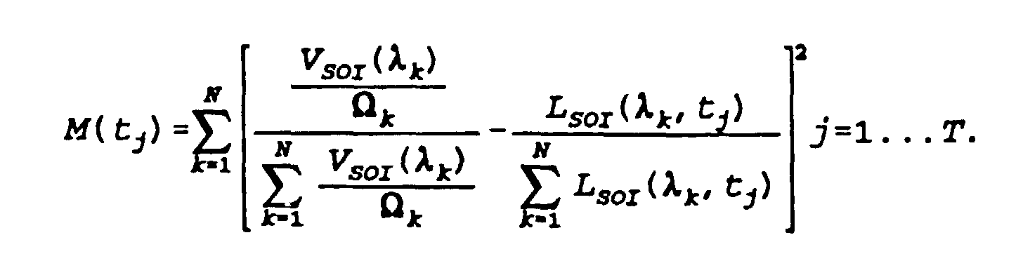
- measured data from one pixel consists of N digitized values V 1 ...V N at the wavelengths ⁇ 1 ... ⁇ N and corresponding library reflectances for any pixel are computed as shown in a step 61.
- the measured quantity (F i ) within the brackets on the left hand side of the above merit function is computed as shown in Fig. 4 in a step 66.
- the corresponding computed quantity (L i ) on the right hand side of the merit function is computed as shown in a step 68.
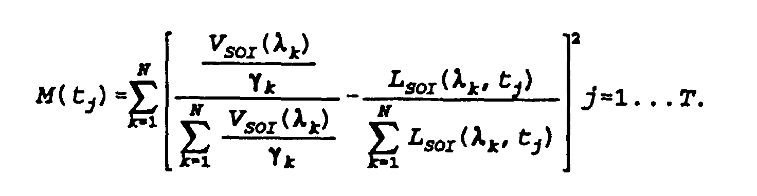
- the factors ⁇ k are pre-measured spectral shape factors (corresponding to factors S 1 , S 2 , . . ., S N shown in a step 70 in Fig. 4) used to relate the voltage to reflectance for each wavelength as shown in a step 72. However, they can themselves be normalized to any wavelength to provide a dimensionless set of spectral shape factors ⁇ 1 ... ⁇ N . as shown below.
- the merit function as shown in the step 62 in Fig. 4, can thus be written in terms of these normalized spectral shape factors ( ⁇ k ) as follows: It should be realized that the above merit function contains only measured data from a single pixel together with computed library patterns L SOI ( ⁇ k ,t j ) which are functionally of the same form as the ratios of the measured data.
- the N spectral shape calibration factors ( ⁇ 1 ,..., ⁇ N ) are obtained from single point measurements on a known reflector such as shown in Fig. 3 as a small bare silicon mirror 56 in the instrument field and need only be made occasionally since the measured ratios inside the merit function are independent of intensity variations and non-uniform illumination problems. This scheme eliminates the need to record full images of a bare silicon calibration wafer.
- the computation of the merit function shown in step 62 of Fig. 4 is, as suggested, a repetitive computation over a large number of possible thicknesses.
- This is shown in Fig. 4 by showing a comparison loop comprising the steps 74, 62, 76, 78 whereby a new normalized spectral pattern is selected from the library in a step 74 according to a step 78 which indicates that a thickness index has changed in response to a determination in a step 76 that the next thickness pattern needs to be compared. This would be done, for example, in steps of 10 ⁇ all the way from 10 microns down to zero thickness. After all these thicknesses have been compared, a step 80 determines the best fit and hence the actual thickness for a pixel. The whole process is then repeated for the next pixel, and so on, until the entire wafer surface has its thickness determined.
- the above description was primarily made in the context of a particular embodiment but that the invention is not limited thereto. Indeed, the invention can be used for determining an unknown layer thickness among any number of layers, provided all the other layers' thicknesses are known and the optical properties of all layers are accurately known.
Landscapes
- Physics & Mathematics (AREA)
- General Physics & Mathematics (AREA)
- Length Measuring Devices By Optical Means (AREA)
- Testing Or Measuring Of Semiconductors Or The Like (AREA)
Description


Claims (26)
- An apparatus for measuring the thickness of a layer of material (24) having front and rear surfaces, said material having a property that will transmit radiation, said apparatus comprising:means (10, 12, 14, 16, 17, 18, 20, 22) for irradiating a front surface area (46) of said layer (24) with a collimated monochromatic radiation (23) so that reflected radiation (29) from said front and rear surfaces has characteristics (R) corresponding to said thickness of said layer (24) in said surface area and wherein saidmeans (10, 12, 14, 16, 17, 18, 20, 22) for irradiating with monochromatic radiation (23) comprises means (17, 189 for sequentially irradiating said surface area with monochromatic light of differing wavelengths, so that ambiguities arising when said thickness is a multiple of a wavelength are eliminated;means (30, 31; 61) for receiving said reflected radiation (29) and for detecting said characteristics (Rm) at said differing wavelengths; charcterized bymeans (34, 36) for self-normalizing each detected characteristics (Rm) at a given wavelength with respect to the characteristics (Rm) detected at all wavelengths and for comparing said self-normalized characteristics (Fi) of said received radiation with a set of reference characteristics (Rc) corresponding to known thicknesses and for providing an output corresponding to said thickness of said layer in said area.
- The apparatus of claim 1, wherein said detected characteristics at all said wavelengths are self-normalized by dividing each detected characteristic (Rm) at a given wavelength by a sum of all detected characteristics (Rm) at all said wavelengths.
- An apparatus as described in claim 1, wherein said set of reference characteristics (Rc) is computed based on predetermined thicknesses and assumed optical properties of the material.
- An apparatus as described in claim 1, wherein said characteristics corresponding to said thickness of said layer comprise a reflectance (R) of said material and said means for receiving (30, 31; 61) said reflected radiation comprises a charge coupled device (30).
- An apparatus as described in claim 4, wherein said means (34, 36) for self-normalizing and comparing said detected characteristics comprises:digitizing means (34) for digitizing said output signal of said charge coupled device (30); andcomputing means (36) for self-normalizing said digitized output signal and for comparing said self-normalized digitized signal with a set of digitized signals corresponding to said reference characteristics.
- An apparatus as described in claim 1, wherein said means (34, 36) for self-normalizing is also for self-normalizing said reference characteristics for comparison with said self-normalized detected characteristics.
- An apparatus as described in claim 1, wherein said set of reference characteristics (Rc) used in said means (34, 36) for comparing is computed based on predetermined thicknesses and assumed properties of said material.
- An apparatus for measuring the thickness of a layer (24) of material having front and rear surfaces, said layer (24) being one of a plurality of layers (42, 40) each having front and rear surfaces and formed on a front surface of a substrate (44), said material having properties that will transmit light, said apparatus comprising:means (10, 12, 14, 16) for providing a beam (19) of collimated light;means (18) for inserting in said beam (19) of collimated light a plurality of narrow band filters (17), each filter (17) passing a single wavelength so that said beam (19) of collimated light becomes monochromatic and that said layer (24) is irradiated with monochromatic ligth of differing wavelengths;means (20) for expanding said beam (19, 23) of collimated light so as to irradiate an entirety of said front surface of said layer (24), said light being reflected off said front and rear surfaces of said layer (24) and said front and rear surfaces of said plurality of other layers (40, 42) and the front surface of the substrate (44), said reflected light interacting to form a fringe pattern an image of which is reflected;means (25, 28; 60, 64) for directing said image of said reflected fringe pattern onto an active surface (31) of a charge coupled device camera (30), said camera (30) providing an output corresponding to said fringe pattern;means (34) for digitizing said output of said charge coupled device camera (30); characterized bymeans (34, 36) for receiving said digitized output of said charged coupled device camera (30) for self-normalizing said digitized output (Rm) for a given wavelength with respect to other digitized outputs at all wavelengths and for comparing said self-normalized output (Fi) with a set of stored self-normalized reference characteristics (Rc) corresponding to known layer thicknesses and for providing an output corresponding to a thickness map of said layer thickness.
- The apparatus of claim 8, wherein said self-normalized digitized output is obtained by dividing each detected characteristic (Rm) at a given wavelength by a sum of all detected characteristics at all wavelengths.
- A method for measuring the thickness of a layer of material (24) having front and rear surfaces, said material having properties that will transmit radiation, said method comprising the steps of:sequentially irradiating a front surface area (46) of said layer (24) with a collimated monochromatic radiation (23) of differing wavelengths so that reflected radiation from said front and rear surfaces has characteristics corresponding to said thickness of said layer in an area and so that ambiguities, arising when said layer thickness is a multiple of a wavelength, are manifested;receiving said reflected radiation (29),detecting said characteristics (Rm) of said received radiation;for each detected characteristic (Rm) at each wavelength, self-normalizing each of said detected characteristics (Rm) at a given wavelength with respect to the characteristics (Rm) detected at all wavelengths to scale each of said detected characteristics (Rm) for comparison with a set of reference characteristics (Rc);comparing said self-normalized detected characteristics (Fi) of said received radiation with said set of reference characteristics (Rc) corresponding to known thicknesses; andproviding an output corresponding to said thickness of said layer (24) in said area based on said comparing of said detected characteristics (Rm) with said set of reference characteristics (Rc).
- A method as described in claim 10, additionally comprising the step of computing said set of reference characteristics (Rc) based on predetermined thicknesses and assumed optical properties of said material; and storing said set of computed reference characteristics (Rc).
- The method as described in claim 10, additionally comprising the step of self-normalizing said set of reference characteristics (Rc) prior to said comparing step.
- A method as'described in claim 10, wherein said step of detecting said characteristics comprises detecting said characteristics (Rm) using a charge coupled device camera (30), said camera providing output signals corresponding to said characteristics and said method further comprising the steps of:digitizing said output signals from said charge coupled device camera (30); andself-normalizing and comparing said digitized signals with a set of digitized reference signals, corresponding to said set of reference characteristics.
- A method as described in claim 13, wherein said characteristic is a reflectance (R) as manifested by said reflected radiation and said charge coupled device camera (30) measures said reflected radiation at a plurality of points to determine said thickness of said layer at said plurality of different points.
- A method as described in claim 10, further comprising the steps of:performing a chemical micropolishing process upon said front surface of said layer (34) in accordance with said output corresponding to said thickness of said layer; andrepeating said above mentioned steps sequentially until said thickness of said layer corresponds to a predetermined value.
- The method of claim 10, wherein said step of self-normalizing comprises the step (66) of dividing each detected characteristic (Rm) by a sum of detected characteristics.
- The method of claim 10, further comprising the step (70, 72) of normalizing said detected characteristics against corresponding pre-measured spectral response characteristics.
- The method of claim 12, wherein said step of self-normalizing said set of reference characteristics comprises the step of dividing each reference characteristic by a sum of reference characteristics.
- A method for measuring the thickness of a layer among one or more layers of known optical properties and thicknesses by comparing, by means of a merit or matching function, a library of computed reflectances (Rc) at different wavelengths with corresponding measured reflectances (Rm) at the different wavelengths, further comprising the steps of:compiling a library of self-normalized computed reflectances (Li) based on the library of computed reflectances (Rc) at each of a plurality of thicknesses at each of the different wavelengths, each of said self-normalized reflectances (Li) being normalized with respect to the reflectances computed for all wavelengths;computing, for each of the measured reflectances (Rm) for each of a plurality of areas of the unknown thickness layer, a self-normalized measured reflectance (Fi) for each of the different wavelengths, self-normalized with respect to the reflectances measured for all wavelengths;computing the merit function, for each area, for each of the plurality of thicknesses, for comparing the self-normlized measured reflectances (Fi) with the library of self-normalized computed reflectances (Li) at each of the plurality of thicknesses; andselecting, for each area, a thickness from the plurality of thicknesses based on the magnitude of the merit function.
- The method of claim 19, wherein said step of compiling is carried out by dividing each computed reflectance (Rc) at each thickness by a sum of computed reflectances for all of the plurality of wavelengths.
- The method of claim 19, further comprising the step of measuring, for a selected reflector (56), a spectral response of the instrument over the different wavelengths and, before computing the self-normalized measured reflectance, normalizing the measured reflectances at each of the different wavelengths with respect to the spectral response of the instrument at the different wavelengths.
- The method of claim 21, wherein said normalizing the measured reflectances (Rm) is carried out by dividing each measured reflectance (Rm) at each wavelength for a given thickness by the measured spectral response of the instrument for that wavelength.
- The method of claim 22, further comprising the step (70, 72) of normalizing the measured spectral response for each wavelength with respect to the measured spectral response for the different wavelengths.
- The method of claim 23, wherein the step of normalizing the measured spectral response for each wavelength is carried out by dividing the measured spectral response for each wavelength by the measured spectral response (Si) for a selected one of the wavelengths.
- The method of claim 19, wherein said step of computing, for each area, a self-normalized measured reflectance for each thickness for each of the different wavelengths is carried out by dividing the measured reflectance for each df the different wavelengths by a sum of measured reflectances.
- The method of claim 21, wherein said step of computing, for each area, a self-normalized measured reflectance for each thickness for each of the different wavelengths is carried out by dividing the measured reflectance for each of the different wavelengths by a sum of normalized measured reflectances.
Applications Claiming Priority (2)
| Application Number | Priority Date | Filing Date | Title |
|---|---|---|---|
| US987926 | 1992-12-10 | ||
| US07/987,926 US5365340A (en) | 1992-12-10 | 1992-12-10 | Apparatus and method for measuring the thickness of thin films |
Publications (2)
| Publication Number | Publication Date |
|---|---|
| EP0601580A1 EP0601580A1 (en) | 1994-06-15 |
| EP0601580B1 true EP0601580B1 (en) | 1998-04-01 |
Family
ID=25533699
Family Applications (1)
| Application Number | Title | Priority Date | Filing Date |
|---|---|---|---|
| EP93119876A Expired - Lifetime EP0601580B1 (en) | 1992-12-10 | 1993-12-09 | Apparatus and method for measuring the thickness of thin films |
Country Status (7)
| Country | Link |
|---|---|
| US (1) | US5365340A (en) |
| EP (1) | EP0601580B1 (en) |
| JP (1) | JPH0830646B2 (en) |
| KR (1) | KR970011746B1 (en) |
| DE (1) | DE69317736T2 (en) |
| IL (1) | IL107901A (en) |
| TW (1) | TW229265B (en) |
Families Citing this family (47)
| Publication number | Priority date | Publication date | Assignee | Title |
|---|---|---|---|---|
| US5555472A (en) * | 1993-12-22 | 1996-09-10 | Integrated Process Equipment Corp. | Method and apparatus for measuring film thickness in multilayer thin film stack by comparison to a reference library of theoretical signatures |
| US6454761B1 (en) | 1995-01-30 | 2002-09-24 | Philip D. Freedman | Laser surgery device and method |
| US5943550A (en) * | 1996-03-29 | 1999-08-24 | Advanced Micro Devices, Inc. | Method of processing a semiconductor wafer for controlling drive current |
| US6366861B1 (en) * | 1997-04-25 | 2002-04-02 | Applied Materials, Inc. | Method of determining a wafer characteristic using a film thickness monitor |
| US6142855A (en) | 1997-10-31 | 2000-11-07 | Canon Kabushiki Kaisha | Polishing apparatus and polishing method |
| US5963329A (en) * | 1997-10-31 | 1999-10-05 | International Business Machines Corporation | Method and apparatus for measuring the profile of small repeating lines |
| US6483580B1 (en) * | 1998-03-06 | 2002-11-19 | Kla-Tencor Technologies Corporation | Spectroscopic scatterometer system |
| US6392756B1 (en) | 1999-06-18 | 2002-05-21 | N&K Technology, Inc. | Method and apparatus for optically determining physical parameters of thin films deposited on a complex substrate |
| US6091485A (en) * | 1999-12-15 | 2000-07-18 | N & K Technology, Inc. | Method and apparatus for optically determining physical parameters of underlayers |
| US7115858B1 (en) | 2000-09-25 | 2006-10-03 | Nanometrics Incorporated | Apparatus and method for the measurement of diffracting structures |
| US7274463B2 (en) * | 2003-12-30 | 2007-09-25 | Sensory Analytics | Anodizing system with a coating thickness monitor and an anodized product |
| US7365860B2 (en) * | 2000-12-21 | 2008-04-29 | Sensory Analytics | System capable of determining applied and anodized coating thickness of a coated-anodized product |
| US6674533B2 (en) | 2000-12-21 | 2004-01-06 | Joseph K. Price | Anodizing system with a coating thickness monitor and an anodized product |
| US20080301954A1 (en) * | 2001-01-22 | 2008-12-11 | Robert Garrett | Air powered roofing saw with gear drive |
| US6898537B1 (en) | 2001-04-27 | 2005-05-24 | Nanometrics Incorporated | Measurement of diffracting structures using one-half of the non-zero diffracted orders |
| DE10123470B4 (en) * | 2001-05-15 | 2010-08-19 | Carl Zeiss Jena Gmbh | Method and arrangement for non-contact determination of product properties |
| US6713753B1 (en) | 2001-07-03 | 2004-03-30 | Nanometrics Incorporated | Combination of normal and oblique incidence polarimetry for the characterization of gratings |
| US6785638B2 (en) * | 2001-08-06 | 2004-08-31 | Timbre Technologies, Inc. | Method and system of dynamic learning through a regression-based library generation process |
| US7061615B1 (en) | 2001-09-20 | 2006-06-13 | Nanometrics Incorporated | Spectroscopically measured overlay target |
| US7286242B2 (en) * | 2001-09-21 | 2007-10-23 | Kmac | Apparatus for measuring characteristics of thin film by means of two-dimensional detector and method of measuring the same |
| US7280230B2 (en) * | 2001-12-19 | 2007-10-09 | Kla-Tencor Technologies Corporation | Parametric profiling using optical spectroscopic systems |
| US6982793B1 (en) | 2002-04-04 | 2006-01-03 | Nanometrics Incorporated | Method and apparatus for using an alignment target with designed in offset |
| US6949462B1 (en) | 2002-04-04 | 2005-09-27 | Nanometrics Incorporated | Measuring an alignment target with multiple polarization states |
| US6992764B1 (en) | 2002-09-30 | 2006-01-31 | Nanometrics Incorporated | Measuring an alignment target with a single polarization state |
| FR2852389B1 (en) * | 2003-03-12 | 2005-05-13 | Commissariat Energie Atomique | METHOD FOR MEASURING THREE DIMENSIONAL OBJECTS BY OPTICAL OMBROSCOPY WITH A SINGLE VIEW |
| US7049156B2 (en) * | 2003-03-19 | 2006-05-23 | Verity Instruments, Inc. | System and method for in-situ monitor and control of film thickness and trench depth |
| KR100546796B1 (en) * | 2003-07-21 | 2006-01-25 | 동부아남반도체 주식회사 | Insulation test method using library of thickness and optical image |
| JP2006041352A (en) * | 2004-07-29 | 2006-02-09 | Dainippon Screen Mfg Co Ltd | Coat inspection device, inspection system, program, coat inspection method and inspection method of printed circuit board |
| US7515253B2 (en) | 2005-01-12 | 2009-04-07 | Kla-Tencor Technologies Corporation | System for measuring a sample with a layer containing a periodic diffracting structure |
| US7038776B1 (en) * | 2005-03-25 | 2006-05-02 | Raytheon Company | Polarimeter to simultaneously measure the stokes vector components of light |
| US7306507B2 (en) | 2005-08-22 | 2007-12-11 | Applied Materials, Inc. | Polishing pad assembly with glass or crystalline window |
| US8260446B2 (en) | 2005-08-22 | 2012-09-04 | Applied Materials, Inc. | Spectrographic monitoring of a substrate during processing using index values |
| US7406394B2 (en) | 2005-08-22 | 2008-07-29 | Applied Materials, Inc. | Spectra based endpointing for chemical mechanical polishing |
| WO2007103304A2 (en) * | 2006-03-07 | 2007-09-13 | Sensory Analytics | A mobile apparatus capable of surface measurements of a coating thickness |
| US7998358B2 (en) | 2006-10-31 | 2011-08-16 | Applied Materials, Inc. | Peak-based endpointing for chemical mechanical polishing |
| US7444198B2 (en) * | 2006-12-15 | 2008-10-28 | Applied Materials, Inc. | Determining physical property of substrate |
| US7952708B2 (en) * | 2007-04-02 | 2011-05-31 | Applied Materials, Inc. | High throughput measurement system |
| US8352061B2 (en) | 2008-11-14 | 2013-01-08 | Applied Materials, Inc. | Semi-quantitative thickness determination |
| US8852175B2 (en) * | 2008-11-21 | 2014-10-07 | Amo Development Llc | Apparatus, system and method for precision depth measurement |
| KR101861834B1 (en) | 2009-11-03 | 2018-05-28 | 어플라이드 머티어리얼스, 인코포레이티드 | Endpoint method using peak location of spectra contour plots versus time |
| US8334986B2 (en) * | 2010-02-25 | 2012-12-18 | Corning Incorporated | Methods and apparatus for the measurement of film thickness |
| DE102013107678A1 (en) * | 2013-07-18 | 2015-01-22 | Technische Universität Darmstadt | Method for determining a layer thickness |
| US10724900B2 (en) * | 2015-09-23 | 2020-07-28 | Filmetrics, Inc. | Determining focus condition in spectral reflectance system |
| JP7481090B2 (en) | 2019-01-09 | 2024-05-10 | 株式会社ディスコ | Thickness measuring device, and processing device equipped with thickness measuring device |
| CN111366478A (en) * | 2020-05-12 | 2020-07-03 | 中国矿业大学(北京) | Electrical measurement-caustic line-digital speckle correlation method synchronous experimental system and method |
| DE102020115544B4 (en) * | 2020-06-11 | 2022-03-31 | Trioptics Gmbh | Measuring device and method for measuring a reflectivity of coated optical elements |
| CN112798614A (en) * | 2020-12-25 | 2021-05-14 | 长江存储科技有限责任公司 | Semiconductor machine and detection method |
Family Cites Families (10)
| Publication number | Priority date | Publication date | Assignee | Title |
|---|---|---|---|---|
| JPS5245455U (en) * | 1975-09-27 | 1977-03-31 | ||
| US4585348A (en) * | 1981-09-28 | 1986-04-29 | International Business Machines Corporation | Ultra-fast photometric instrument |
| JPS6176904A (en) * | 1984-09-21 | 1986-04-19 | Oak Seisakusho:Kk | Method for measuring film thickness |
| US4707611A (en) * | 1986-12-08 | 1987-11-17 | Rockwell International Corporation | Incremental monitoring of thin films |
| JPH01206203A (en) * | 1988-02-12 | 1989-08-18 | Toshiba Corp | Checking method of imperfection of film thickness |
| JPH0252205A (en) * | 1988-08-17 | 1990-02-21 | Dainippon Screen Mfg Co Ltd | Film thickness measuring method |
| JPH0731050B2 (en) * | 1988-12-29 | 1995-04-10 | オリンパス光学工業株式会社 | Optical film thickness measuring device |
| US5042949A (en) * | 1989-03-17 | 1991-08-27 | Greenberg Jeffrey S | Optical profiler for films and substrates |
| JPH0820224B2 (en) * | 1990-06-13 | 1996-03-04 | リソテックジャパン株式会社 | Method of measuring photoresist dissolution rate |
| JPH0817166B2 (en) * | 1991-04-27 | 1996-02-21 | 信越半導体株式会社 | Ultra thin film SOI substrate manufacturing method and manufacturing apparatus |
-
1992
- 1992-12-10 US US07/987,926 patent/US5365340A/en not_active Expired - Lifetime
-
1993
- 1993-12-06 IL IL107901A patent/IL107901A/en not_active IP Right Cessation
- 1993-12-09 DE DE69317736T patent/DE69317736T2/en not_active Expired - Lifetime
- 1993-12-09 TW TW082110456A patent/TW229265B/zh active
- 1993-12-09 EP EP93119876A patent/EP0601580B1/en not_active Expired - Lifetime
- 1993-12-10 JP JP5310844A patent/JPH0830646B2/en not_active Expired - Lifetime
- 1993-12-10 KR KR1019930027149A patent/KR970011746B1/en not_active Expired - Lifetime
Also Published As
| Publication number | Publication date |
|---|---|
| DE69317736D1 (en) | 1998-05-07 |
| DE69317736T2 (en) | 1998-07-30 |
| JPH06281420A (en) | 1994-10-07 |
| KR940016660A (en) | 1994-07-23 |
| IL107901A0 (en) | 1994-04-12 |
| US5365340A (en) | 1994-11-15 |
| JPH0830646B2 (en) | 1996-03-27 |
| IL107901A (en) | 1998-02-08 |
| KR970011746B1 (en) | 1997-07-15 |
| TW229265B (en) | 1994-09-01 |
| EP0601580A1 (en) | 1994-06-15 |
Similar Documents
| Publication | Publication Date | Title |
|---|---|---|
| US5365340A (en) | Apparatus and method for measuring the thickness of thin films | |
| US5333049A (en) | Apparatus and method for interferometrically measuring the thickness of thin films using full aperture irradiation | |
| US5293214A (en) | Apparatus and method for performing thin film layer thickness metrology by deforming a thin film layer into a reflective condenser | |
| EP0577399B1 (en) | Apparatus and method for performing thin film layer thickness metrology on a thin film layer having shape deformations and local slope variations | |
| US5555472A (en) | Method and apparatus for measuring film thickness in multilayer thin film stack by comparison to a reference library of theoretical signatures | |
| US5543919A (en) | Apparatus and method for performing high spatial resolution thin film layer thickness metrology | |
| US5241366A (en) | Thin film thickness monitor | |
| US5337150A (en) | Apparatus and method for performing thin film layer thickness metrology using a correlation reflectometer | |
| US4999014A (en) | Method and apparatus for measuring thickness of thin films | |
| US5856871A (en) | Film thickness mapping using interferometric spectral imaging | |
| CA1164094A (en) | Non-contact measurement of surface profile | |
| US6204922B1 (en) | Rapid and accurate thin film measurement of individual layers in a multi-layered or patterned sample | |
| EP0617255A1 (en) | Apparatus and method for thick wafer measurement | |
| KR20040071146A (en) | Method and apparatus for measuring stress in semiconductor wafers | |
| TW200532164A (en) | Film thickness measuring method and apparatus | |
| JP2010048604A (en) | Apparatus and method for measuring film thickness | |
| US10240981B2 (en) | Optical spectrometer configuration including spatially variable filter (SVF) | |
| IL119299A (en) | Apparatus and method for measuring the thickness of thin films | |
| JPS6271804A (en) | Film thickness measuring instrument |
Legal Events
| Date | Code | Title | Description |
|---|---|---|---|
| PUAI | Public reference made under article 153(3) epc to a published international application that has entered the european phase |
Free format text: ORIGINAL CODE: 0009012 |
|
| AK | Designated contracting states |
Kind code of ref document: A1 Designated state(s): CH DE FR GB LI NL SE |
|
| 17P | Request for examination filed |
Effective date: 19941215 |
|
| 17Q | First examination report despatched |
Effective date: 19960130 |
|
| GRAG | Despatch of communication of intention to grant |
Free format text: ORIGINAL CODE: EPIDOS AGRA |
|
| GRAG | Despatch of communication of intention to grant |
Free format text: ORIGINAL CODE: EPIDOS AGRA |
|
| GRAH | Despatch of communication of intention to grant a patent |
Free format text: ORIGINAL CODE: EPIDOS IGRA |
|
| RAP1 | Party data changed (applicant data changed or rights of an application transferred) |
Owner name: IPEC PRECISION, INC. |
|
| GRAH | Despatch of communication of intention to grant a patent |
Free format text: ORIGINAL CODE: EPIDOS IGRA |
|
| GRAA | (expected) grant |
Free format text: ORIGINAL CODE: 0009210 |
|
| AK | Designated contracting states |
Kind code of ref document: B1 Designated state(s): CH DE FR GB LI NL SE |
|
| PG25 | Lapsed in a contracting state [announced via postgrant information from national office to epo] |
Ref country code: NL Free format text: LAPSE BECAUSE OF FAILURE TO SUBMIT A TRANSLATION OF THE DESCRIPTION OR TO PAY THE FEE WITHIN THE PRESCRIBED TIME-LIMIT Effective date: 19980401 Ref country code: LI Free format text: LAPSE BECAUSE OF FAILURE TO SUBMIT A TRANSLATION OF THE DESCRIPTION OR TO PAY THE FEE WITHIN THE PRESCRIBED TIME-LIMIT Effective date: 19980401 Ref country code: CH Free format text: LAPSE BECAUSE OF FAILURE TO SUBMIT A TRANSLATION OF THE DESCRIPTION OR TO PAY THE FEE WITHIN THE PRESCRIBED TIME-LIMIT Effective date: 19980401 |
|
| REG | Reference to a national code |
Ref country code: CH Ref legal event code: EP |
|
| REF | Corresponds to: |
Ref document number: 69317736 Country of ref document: DE Date of ref document: 19980507 |
|
| PG25 | Lapsed in a contracting state [announced via postgrant information from national office to epo] |
Ref country code: SE Free format text: LAPSE BECAUSE OF FAILURE TO SUBMIT A TRANSLATION OF THE DESCRIPTION OR TO PAY THE FEE WITHIN THE PRESCRIBED TIME-LIMIT Effective date: 19980701 |
|
| ET | Fr: translation filed | ||
| NLV1 | Nl: lapsed or annulled due to failure to fulfill the requirements of art. 29p and 29m of the patents act | ||
| REG | Reference to a national code |
Ref country code: CH Ref legal event code: PL |
|
| PLBE | No opposition filed within time limit |
Free format text: ORIGINAL CODE: 0009261 |
|
| STAA | Information on the status of an ep patent application or granted ep patent |
Free format text: STATUS: NO OPPOSITION FILED WITHIN TIME LIMIT |
|
| 26N | No opposition filed | ||
| REG | Reference to a national code |
Ref country code: GB Ref legal event code: IF02 |
|
| PGFP | Annual fee paid to national office [announced via postgrant information from national office to epo] |
Ref country code: GB Payment date: 20031203 Year of fee payment: 11 |
|
| PG25 | Lapsed in a contracting state [announced via postgrant information from national office to epo] |
Ref country code: GB Free format text: LAPSE BECAUSE OF NON-PAYMENT OF DUE FEES Effective date: 20041209 |
|
| GBPC | Gb: european patent ceased through non-payment of renewal fee |
Effective date: 20041209 |
|
| PGFP | Annual fee paid to national office [announced via postgrant information from national office to epo] |
Ref country code: FR Payment date: 20130110 Year of fee payment: 20 |
|
| PGFP | Annual fee paid to national office [announced via postgrant information from national office to epo] |
Ref country code: DE Payment date: 20121231 Year of fee payment: 20 |
|
| REG | Reference to a national code |
Ref country code: DE Ref legal event code: R071 Ref document number: 69317736 Country of ref document: DE |
|
| PG25 | Lapsed in a contracting state [announced via postgrant information from national office to epo] |
Ref country code: DE Free format text: LAPSE BECAUSE OF EXPIRATION OF PROTECTION Effective date: 20131210 |
|
| P01 | Opt-out of the competence of the unified patent court (upc) registered |
Effective date: 20230525 |