EP0599468B1 - Chemical-vapor-deposition-produced silicon carbide - Google Patents
Chemical-vapor-deposition-produced silicon carbide Download PDFInfo
- Publication number
- EP0599468B1 EP0599468B1 EP93307966A EP93307966A EP0599468B1 EP 0599468 B1 EP0599468 B1 EP 0599468B1 EP 93307966 A EP93307966 A EP 93307966A EP 93307966 A EP93307966 A EP 93307966A EP 0599468 B1 EP0599468 B1 EP 0599468B1
- Authority
- EP
- European Patent Office
- Prior art keywords
- sic
- deposition
- less
- cvd
- attenuation coefficient
- Prior art date
- Legal status (The legal status is an assumption and is not a legal conclusion. Google has not performed a legal analysis and makes no representation as to the accuracy of the status listed.)
- Expired - Lifetime
Links
Images



Classifications
-
- C—CHEMISTRY; METALLURGY
- C04—CEMENTS; CONCRETE; ARTIFICIAL STONE; CERAMICS; REFRACTORIES
- C04B—LIME, MAGNESIA; SLAG; CEMENTS; COMPOSITIONS THEREOF, e.g. MORTARS, CONCRETE OR LIKE BUILDING MATERIALS; ARTIFICIAL STONE; CERAMICS; REFRACTORIES; TREATMENT OF NATURAL STONE
- C04B35/00—Shaped ceramic products characterised by their composition; Ceramics compositions; Processing powders of inorganic compounds preparatory to the manufacturing of ceramic products
- C04B35/515—Shaped ceramic products characterised by their composition; Ceramics compositions; Processing powders of inorganic compounds preparatory to the manufacturing of ceramic products based on non-oxide ceramics
- C04B35/56—Shaped ceramic products characterised by their composition; Ceramics compositions; Processing powders of inorganic compounds preparatory to the manufacturing of ceramic products based on non-oxide ceramics based on carbides or oxycarbides
- C04B35/565—Shaped ceramic products characterised by their composition; Ceramics compositions; Processing powders of inorganic compounds preparatory to the manufacturing of ceramic products based on non-oxide ceramics based on carbides or oxycarbides based on silicon carbide
- C04B35/571—Shaped ceramic products characterised by their composition; Ceramics compositions; Processing powders of inorganic compounds preparatory to the manufacturing of ceramic products based on non-oxide ceramics based on carbides or oxycarbides based on silicon carbide obtained from Si-containing polymer precursors or organosilicon monomers
-
- C—CHEMISTRY; METALLURGY
- C23—COATING METALLIC MATERIAL; COATING MATERIAL WITH METALLIC MATERIAL; CHEMICAL SURFACE TREATMENT; DIFFUSION TREATMENT OF METALLIC MATERIAL; COATING BY VACUUM EVAPORATION, BY SPUTTERING, BY ION IMPLANTATION OR BY CHEMICAL VAPOUR DEPOSITION, IN GENERAL; INHIBITING CORROSION OF METALLIC MATERIAL OR INCRUSTATION IN GENERAL
- C23C—COATING METALLIC MATERIAL; COATING MATERIAL WITH METALLIC MATERIAL; SURFACE TREATMENT OF METALLIC MATERIAL BY DIFFUSION INTO THE SURFACE, BY CHEMICAL CONVERSION OR SUBSTITUTION; COATING BY VACUUM EVAPORATION, BY SPUTTERING, BY ION IMPLANTATION OR BY CHEMICAL VAPOUR DEPOSITION, IN GENERAL
- C23C16/00—Chemical coating by decomposition of gaseous compounds, without leaving reaction products of surface material in the coating, i.e. chemical vapour deposition [CVD] processes
- C23C16/01—Chemical coating by decomposition of gaseous compounds, without leaving reaction products of surface material in the coating, i.e. chemical vapour deposition [CVD] processes on temporary substrates, e.g. substrates subsequently removed by etching
-
- C—CHEMISTRY; METALLURGY
- C23—COATING METALLIC MATERIAL; COATING MATERIAL WITH METALLIC MATERIAL; CHEMICAL SURFACE TREATMENT; DIFFUSION TREATMENT OF METALLIC MATERIAL; COATING BY VACUUM EVAPORATION, BY SPUTTERING, BY ION IMPLANTATION OR BY CHEMICAL VAPOUR DEPOSITION, IN GENERAL; INHIBITING CORROSION OF METALLIC MATERIAL OR INCRUSTATION IN GENERAL
- C23C—COATING METALLIC MATERIAL; COATING MATERIAL WITH METALLIC MATERIAL; SURFACE TREATMENT OF METALLIC MATERIAL BY DIFFUSION INTO THE SURFACE, BY CHEMICAL CONVERSION OR SUBSTITUTION; COATING BY VACUUM EVAPORATION, BY SPUTTERING, BY ION IMPLANTATION OR BY CHEMICAL VAPOUR DEPOSITION, IN GENERAL
- C23C16/00—Chemical coating by decomposition of gaseous compounds, without leaving reaction products of surface material in the coating, i.e. chemical vapour deposition [CVD] processes
- C23C16/22—Chemical coating by decomposition of gaseous compounds, without leaving reaction products of surface material in the coating, i.e. chemical vapour deposition [CVD] processes characterised by the deposition of inorganic material, other than metallic material
- C23C16/30—Deposition of compounds, mixtures or solid solutions, e.g. borides, carbides, nitrides
- C23C16/32—Carbides
- C23C16/325—Silicon carbide
-
- C—CHEMISTRY; METALLURGY
- C23—COATING METALLIC MATERIAL; COATING MATERIAL WITH METALLIC MATERIAL; CHEMICAL SURFACE TREATMENT; DIFFUSION TREATMENT OF METALLIC MATERIAL; COATING BY VACUUM EVAPORATION, BY SPUTTERING, BY ION IMPLANTATION OR BY CHEMICAL VAPOUR DEPOSITION, IN GENERAL; INHIBITING CORROSION OF METALLIC MATERIAL OR INCRUSTATION IN GENERAL
- C23C—COATING METALLIC MATERIAL; COATING MATERIAL WITH METALLIC MATERIAL; SURFACE TREATMENT OF METALLIC MATERIAL BY DIFFUSION INTO THE SURFACE, BY CHEMICAL CONVERSION OR SUBSTITUTION; COATING BY VACUUM EVAPORATION, BY SPUTTERING, BY ION IMPLANTATION OR BY CHEMICAL VAPOUR DEPOSITION, IN GENERAL
- C23C16/00—Chemical coating by decomposition of gaseous compounds, without leaving reaction products of surface material in the coating, i.e. chemical vapour deposition [CVD] processes
- C23C16/44—Chemical coating by decomposition of gaseous compounds, without leaving reaction products of surface material in the coating, i.e. chemical vapour deposition [CVD] processes characterised by the method of coating
- C23C16/4401—Means for minimising impurities, e.g. dust, moisture or residual gas, in the reaction chamber
- C23C16/4404—Coatings or surface treatment on the inside of the reaction chamber or on parts thereof
-
- C—CHEMISTRY; METALLURGY
- C01—INORGANIC CHEMISTRY
- C01P—INDEXING SCHEME RELATING TO STRUCTURAL AND PHYSICAL ASPECTS OF SOLID INORGANIC COMPOUNDS
- C01P2006/00—Physical properties of inorganic compounds
- C01P2006/40—Electric properties
-
- Y—GENERAL TAGGING OF NEW TECHNOLOGICAL DEVELOPMENTS; GENERAL TAGGING OF CROSS-SECTIONAL TECHNOLOGIES SPANNING OVER SEVERAL SECTIONS OF THE IPC; TECHNICAL SUBJECTS COVERED BY FORMER USPC CROSS-REFERENCE ART COLLECTIONS [XRACs] AND DIGESTS
- Y10—TECHNICAL SUBJECTS COVERED BY FORMER USPC
- Y10S—TECHNICAL SUBJECTS COVERED BY FORMER USPC CROSS-REFERENCE ART COLLECTIONS [XRACs] AND DIGESTS
- Y10S438/00—Semiconductor device manufacturing: process
- Y10S438/931—Silicon carbide semiconductor
-
- Y—GENERAL TAGGING OF NEW TECHNOLOGICAL DEVELOPMENTS; GENERAL TAGGING OF CROSS-SECTIONAL TECHNOLOGIES SPANNING OVER SEVERAL SECTIONS OF THE IPC; TECHNICAL SUBJECTS COVERED BY FORMER USPC CROSS-REFERENCE ART COLLECTIONS [XRACs] AND DIGESTS
- Y10—TECHNICAL SUBJECTS COVERED BY FORMER USPC
- Y10T—TECHNICAL SUBJECTS COVERED BY FORMER US CLASSIFICATION
- Y10T428/00—Stock material or miscellaneous articles
- Y10T428/26—Web or sheet containing structurally defined element or component, the element or component having a specified physical dimension
Definitions
- the present invention is directed to silicon carbide produced by chemical vapor deposition processes having improved optical properties, including improved optical transmission, purity, and electrical resistivity, and to a deposition process for producing such silicon carbide.
- LIDAR light detection and ranging
- Known bulk silicon carbide is almost invariably opaque, absorbing and scattering light in the visible and infrared regions of the spectrum.
- Methods of producing bulk SiC include sintering and hot pressing, slip casting and reaction bonding. These methods are unlikely candidates for producing optically transmitting SiC as they suffer from one or more of the following drawbacks: 1) they produce a multi-phase material, e.g., include a Si phase, 2) the material is not theoretically dense, and/or 3) the material is not of high purity and may contain metallic impurities that degrade optical transmission.
- SiC optically transmitting SiC
- CVD chemical vapor deposition
- most of the SiC previously produced by CVD is opaque, exhibiting considerable scattering and absorption in the visible and infrared.
- Applicants are aware of efforts by the U.S. Air Force and General Electric to improve the infrared transmission of SiC by improving process parameters, such as substrate temperature, flow rates, furnace pressure etc. These efforts met with limited success.
- SiC transmitted in the 2-5 ⁇ m (infrared spectrum range) the material exhibited considerable scattering which made it unsuitable for use in imaging applications.
- Chinone et al, Extended Abstracts Vol 89/2, 1989, p.726, disclose the manufacture of polycrystalline SiC wafers by a CVD process using methyltrichlorosilane (MTS) and hydrogen gas at 1523-1623K, at a deposition rate of 0.08 to 1 mm/h.
- MTS methyltrichlorosilane
- EP-A-494753 discloses a method for enhancing the infrared transmission of CVD-produced SiC by annealing at temperatures from 1800 to 2600°C.
- Other objects include providing CVD-SiC having heretofore unachieved purity, and electrical resistivity.
- polycrystalline chemical vapor deposited ⁇ -SiC having an attenuation coefficient at 0.6328 ⁇ m of 20 cm -1 or less, an attenuation coefficient at 3 ⁇ m of 21 cm -1 or less and a thickness of greater than 0.1 mm.
- the ⁇ -SiC of the invention preferably has an attenuation coefficient at 3 ⁇ m of 2.8 cm -1 or less.
- a method of producing optically transmitting free-standing ⁇ -SiC in a chemical vapor deposition apparatus having a deposition chamber with a surface therein for deposition of SiC by introducing methyltrichlorosilane and H 2 gas into said reaction chamber under conditions which pyrolytically deposit silicon carbide on said surface, characterised in that said conditions comprise a deposition chamber temperature of between 1400°C and 1500°C, a deposition chamber pressure of 6.67kPa (50 torr) or less, a H 2 /methyltrichlorosilane molar ratio of between 4:1 and 30:1 and a deposition rate of 1 ⁇ m per minute or less.
- Silicon carbide fabricated by the chemical vapor deposition (CVD) process of the invention, is optically transmitting in the visible and infrared range. Specific deposition parameters are required to produce the optically transmitting silicon carbide. This silicon carbide is highly pure, theoretically dense and has electrical resistivity in excess of SiC's previously known.
- Fig. 1 is a schematic of CVD apparatus used to fabricate optically transmitting ⁇ -SiC.
- Fig. 2 is a graph comparing the transmission of CVD- ⁇ -SiC with the transmission of ⁇ -SiC.
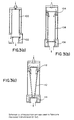
- Figs. 3a, 3b and 3c illustrate different baffle/mandrel arrangements used within the deposition fpchamber of a furnace for the fabrication of CVD- ⁇ -SiC.
- Fig. 4 is a transmission spectrum of a highly optically transmitting CVD- ⁇ -SiC.
- properties of SiC produced in accordance with the invention are room temperature values, i.e., measured at 20-28°C (293-301 K). Although it is believed that thermal conductivity measurements are generally independent of the measuring technique, thermal conductivity values reported herein are those measured by flash-lamp techniques. Deposition chamber temperatures are measured by thermal probes within the deposition chamber placed closely adjacent the deposition site, e.g., a mandrel on which bulk free-standing SiC is to be deposited or a surface on which a film of SiC is to be deposited.
- the deposition site temperature may not be exactly that of the probe-measured location, experience has found that probes closely adjacent, but differently located relative to a deposition site are almost always within 10°C of each other and generally within 5°C of each other. Thus, the deposition site is presumed to be within 5-10°C of the probed deposition chamber temperature.
- the SiC to which the invention pertains is bulk or free-standing, i.e., capable of being self-supported. This is to be distinguished from thin SiC films which are deposited upon a surface with the intent that the SiC remain permanently bonded thereto. To be free-standing, the SiC must generally be deposited to a thickness of upward of 0.1 mm.
- Silicon carbide produced in accordance with the present invention has an attenuation coefficient at 0.6328 ⁇ m of 20 cm -1 or less, preferably about 10 or less, and more preferably about 8 or less.
- the silicon carbide has an attenuation coefficient at 3 ⁇ m of 21 cm -1 or less, preferably 2.8 cm -1 or less and more preferably 2.1 cm -1 or less. It is believed that silicon carbide produced in accordance with the present invention is more optically transmitting at 0.6328 and 3 ⁇ m than any polycrystalline silicon carbide of the prior art.
- the silicon carbide in accordance with the invention is stoichiometric (1:1 Si:C ratio), 100% theoretical dense, and highly pure, i.e., about 5 ppm metallic impurities or less and preferably about 3.5 ppm metallic impurities or less. It is found that the higher is the purity, the greater is the optical transmittance of the SiC produced. Also high purity is very important for semiconductor furniture manufactured of CVD-SiC. High purity is achieved using high purity reaction materials, particularly 0 2 -free H 2 and contamination free graphite deposition set up. It has been demonstrated that distilling MTS from its aspurchased condition results in more optically transmitting CVD-deposited SiC.
- SiC of the present invention Another feature of the SiC of the present invention is its very high bulk resistivity. Resistivity is an important attribute of material for electronic packaging.
- the upper limit of most non-doped SiC to date is about 100 ohm-cm, and CVD-SiC is not believed to have been consistently produced having resistivity of more than 100 ohm-cm.
- the resistivity of CVD-SiC according to the present invention has reached 4.53x10 4 ohm-cm.
- novel CVD-SiC is produced in accordance with the present invention having resistivity of 500 ohm-cm or greater, preferably 1000 ohm-cm or greater, and more preferably 10,000 ohm-cm or greater.
- the SiC produced in accordance with the invention is of the n-type, whereas most CVD-SiC is of the p-type. n-type is preferred as its resistivity tends to be constant over a broader temperature range.
- Fig. 1 Illustrated in Fig. 1 is an apparatus useful for fabricating CVD- ⁇ -SiC. Deposition is carried out within a furnace 10. A stainless steel wall provides a cylindrical deposition chamber 12. Heating is provided by a graphite heating element 14 which is connected to an external power supply by an electrode 16. Graphite deposition mandrels 18 are arranged within a graphite isolation tube 20 and gas is introduced by means of an injector 22 through the upper end of the isolation tube so that the reaction gases sweep along the mandrels 18. One or more baffle(s) 24 is used to control the aerodynamics of gas flow through the furnace.
- the line 26 which supplies the injector is fed by an argon cylinder 28, a hydrogen cylinder 30, and a MTS bubbler 32.
- the argon is fed by lines 34 and 36 both directly to inlet line 26 and through the bubbler 32.
- the hydrogen cylinder is connected by a line 38 to the inlet line 26.
- Argon flow through lines 32 and 36 and hydrogen flow through line 38 are controlled by mass flow controllers 40, 42 and 44.
- the MTS cylinder 32 is maintained at a constant temperature by a constant temperature bath 46.
- a pressure gauge 48 is connected to a feed back loop which controls the gas pressure of the bubbler 32.
- An outlet line 50 is connected to a bottom outlet port 51.
- Pressure within the deposition chamber 12 is controlled by a vacuum pump 52 which pulls gases through the chamber and a furnace pressure control valve 54 operably connected to the vacuum pump.
- the temperature and pressure within the deposition chamber 12 are measured by a thermal probe 58 and a pressure indicator 56.
- Exhaust gases are passed through a filter 60 to remover particulate material upstream of the pressure control valve and through a scrubber 62 downstream of the vacuum pump to remove HCl.
- the arrangement of baffles may be varied to produce desired results.
- the results discussed below with respect to Figs 3a, 3b and 3c are particular to the furnace in which the SiC was deposited and may vary from furnace to furnace and also the configuration of the mandrel or substrate on which SiC of desired configuration is to be deposited.
- a deposition chamber temperature of between 1400 and 1500°C, preferably between 1400 and 1450°C is employed.
- the deposition chamber pressure is 6.67 kPa (50 torr) or lower, preferably 1.33 kPa (10 torr) or lower and most preferably 667 Pa (5 torr) or lower.
- the H 2 /MTS ratio is from 4:1 to 30:1, preferably from 10:1 to 20:1.
- the deposition rate is 1 ⁇ m per minute or less; it is believed that this very low deposition rate is critical to obtain ⁇ -SiC with good optical transmittance.
- the rate at which the deposition surface is swept by the reactant gases also appears to affect the optical transmittance of the deposited SiC.
- optically transmitting SiC has been produced with average flow velocities of about 10 cm/sec, it is preferred that flow velocities be at least 300 cm/sec, and more preferably at least 1000 cm/sec.
- Sweep velocity which is the gas velocity at the deposition surface, is a function not only of the flow rate of gases into the furnace, but of the furnace design and orientation of the deposition surface(s) within the deposition chamber of the furnace.
- HCl is a reaction product of the deposition of SiC using MTS and H2 as the reaction gases. It is found that adding gaseous HCl to the gas stream that is introduced into the reaction chamber further improves the optical transmission of the CVD- ⁇ -SiC which is produced. To have a significant effect on transmission of the SiC, the HCl/MTS molar ratio is generally at least 0.2:1.
- the CVD-SiC was characterized for vis-IR transmission.
- the SiC transmission was determined to be dependent upon MTS purity, CVD process conditions and CVD deposition geometry.
- the commercially available MTS of 99% purity contains metallic impurities which end up in the CVD-SiC and degrade its near-IR transmission. Distillation of MTS in a narrow temperature range around its boiling point has resulted in fabricating SiC which exhibits good transmission in the infrared region.
- Two deposition set-ups were tried in an effort to maximize the transmission of CVD-SiC. These set-ups are shown in Figure 3a, 3b and 3c. All these set-ups yielded CVD- ⁇ -SiC with improved transmission at different parts of the deposition region.
- Two set-ups (Figs. 3a,b) used four rectangular mandrel plates, 8.9 cm (3.5 in.)-wide x 30.5 cm (12 in.)-long, arranged in the form of an open square box.
- the deposition set-up of Figure 3a consisted of a mandrel box 100 at the end of which was placed a graphite baffle 102.
- porous material was deposited on the mandrel while dense and good quality ⁇ -SiC was obtained on the baffle. It is believed that the porous material was deposited because (i) the reagents were "cold," i.e., there was considerable temperature difference between the mandrel and the gaseous reagents and (ii) the reagent sweep speed on the mandrel walls was small. This explanation is consistent with the observation that the material on the upper half of the mandrel was more porous than on the lower half.
- FIG. 3b two baffles were used, one 104 before and the other 106 after the mandrel box.
- the function of the first baffle 104 is to preheat the reagents and direct the gas close to the mandrel walls to increase reagents sweep speed along the mandrel box 108.
- This deposition set-up produced CVD ⁇ -SiC with good vis-IR transmission.
- the "best" material was produced on the upper half of the the mandrel box. The deposited material on other areas had better transmission than that produced at other CVD conditions.
- the two walls of the mandrel box 110 were tapered.
- the cross-section of the mandrel box was a square 8.9 cm x 8.9 cm (3.5 in. x 3.5 in.) on the top end and a rectangle 8.9 cm x 2.7 cm (3.5 in. x 1.05 in.) at the bottom end.
- the aim of using this tapered box was to continuously reduce the cross-section and thus increase the flow velocity to study its effect on the quality of the material.
- This set-up also employed a baffle 112 before and a baffle 114 after the mandrel box. Although this configuration also produced good optical quality CVD-SiC, considerable stress in the material was observed and the deposited material exhibited substantial bowing.
- Table 2 below lists the attenuation coefficient values that were obtained when HCl was added to the reagent mixture.
- a comparison of attenuation coefficient for Run #10 and #11 clearly shows improved optical transmission values when HCl is added.
- the vis-IR transmittance of CVD-SiC increased as the furnace pressure decreased.
- Furnace Setup Furnace Pressure (Torr) (Pa) Attenuation Coefficient (cm) Average flow Velocity cm/sec @ 0.6328 ⁇ m @ 3 ⁇ m 9 3b 7 933 7.4 2.8 540 10 3b 3 400 6.9 2.1 1260
- Figure 2 shows a comparison of transmission of ⁇ -SiC with that of commercially available ⁇ -SiC single crystal sample. Both samples are 0.305 mm (0.012-inch) thick. It is seen that CVD- ⁇ SiC performs considerably better than single crystal ⁇ -SiC in the near-IR region while the latter material performs better in the visible region.
- Figure 4 shows infrared transmission of CVD-SiC when HCl is added to the reaction mixture (Run #10).
- the thickness of the sample was about 0.56 mm (0.022-inch).
- 60% transmission is seen in the near IR region which corresponds to an attenuation coefficient of 2.1 cm -1 at 3 ⁇ m. This is believed to be the lowest value of specular attenuation coefficient that has ever been achieved for polycrystalline CVD- ⁇ SiC free-standing sample.
Landscapes
- Chemical & Material Sciences (AREA)
- Engineering & Computer Science (AREA)
- Materials Engineering (AREA)
- Organic Chemistry (AREA)
- General Chemical & Material Sciences (AREA)
- Chemical Kinetics & Catalysis (AREA)
- Mechanical Engineering (AREA)
- Metallurgy (AREA)
- Ceramic Engineering (AREA)
- Inorganic Chemistry (AREA)
- Structural Engineering (AREA)
- Manufacturing & Machinery (AREA)
- Carbon And Carbon Compounds (AREA)
- Chemical Vapour Deposition (AREA)
- Ceramic Products (AREA)
- Producing Shaped Articles From Materials (AREA)
Description
| Attenuation Coefficient of CVD-βSiC as Function of Furnace Pressure | ||||||
| Run No. | Furnace Set-Up | Furnace Pressure (Torr) | (kPa) | Attenuation Coefficient (cm-1) | Avg. flow Velocity cm/sec | |
| @ 0.6328 µm | @ 3µm | |||||
| Ref. 2 | 3a | 200 | 26.7 | 30 | 40 | 49 |
| Ref. 3 | 3b | 200 | 26.7 | 66 | 24 | 21 |
| 4 | | 40 | 5.33 | 19 | 21 | 197 |
| 5 | 3c | 20 | 2.67 | 16 | 14 | 272-761 |
| 7 | | 10 | 1.33 | 7.3 | 3.5 | 365 |
| 11 | 3b | 3 | 0.40 | - | 7.6 | 1260 |
| Ref: Reference example |
| Attenuation Coefficient of CVD-βSiC when HCl is Added to the Reaction Mixture | ||||||
| Run No. | Furnace Setup | Furnace Pressure (Torr) | (Pa) | Attenuation Coefficient (cm) | Average flow Velocity cm/sec | |
| @ 0.6328 µm | @ | |||||
| 9 | 3b | 7 | 933 | 7.4 | 2.8 | 540 |
| 10 | 3b | 3 | 400 | 6.9 | 2.1 | 1260 |
Claims (9)
- Polycrystalline chemical vapor deposited β-SiC having an attenuation coefficient at0.6328 µm of 20 cm-1 or less, an attenuation coefficient at 3 µm of 21 cm-1 or less and a thickness of greater than 0.1 mm.
- β-SiC according to claim 1 having an attenuation coefficient at 0.6328 µm of 10 cm-1 or less, preferably 8 cm-1 or less.
- β-SiC according to claim 1 or claim 2 having an attenuation coefficient at 3 µm of 2.8 cm-1 or less.
- β-SiC according to claim 3 having an attenuation coefficient at 3 µm of 2.1 cm-1 or less.
- A method of producing optically transmitting free-standing β-SiC in a chemical vapor deposition apparatus (10) having a deposition chamber (12) with a surface therein for deposition of SiC, by introducing methyltrichlorosilane and H2 gas into said reaction chamber under conditions which pyrolytically deposit silicon carbide on said surface, characterised in that said conditions comprise a deposition chamber temperature of between 1400°C and 1500°C, a deposition chamber pressure of 6.67kPa (50 torr) or less, a H2/methyltrichlorosilane molar ratio of between 4:1 and 30:1 and a deposition rate of 1 µm per minute or less.
- A method according to claim 5 wherein said pressure is 1.33kPa (10 torr) or less, preferably 667Pa (5 torr) or less.
- A method according to claim 5 or claim 6 wherein said temperature is between 1400°C and 1450°C.
- A method according to any one of claims 5 to 7 wherein said H2/methyltrichlorosilane ratio is between 10:1 and 20:1.
- A method according to any one of claims 5 to 8 wherein HCl is supplied to said deposition chamber to give an HCl/methyltrichlorosilane molar ratio of at least 0.2:1.
Applications Claiming Priority (2)
| Application Number | Priority Date | Filing Date | Title |
|---|---|---|---|
| US97996592A | 1992-11-23 | 1992-11-23 | |
| US979965 | 1992-11-23 |
Publications (2)
| Publication Number | Publication Date |
|---|---|
| EP0599468A1 EP0599468A1 (en) | 1994-06-01 |
| EP0599468B1 true EP0599468B1 (en) | 1998-01-07 |
Family
ID=25527249
Family Applications (1)
| Application Number | Title | Priority Date | Filing Date |
|---|---|---|---|
| EP93307966A Expired - Lifetime EP0599468B1 (en) | 1992-11-23 | 1993-10-07 | Chemical-vapor-deposition-produced silicon carbide |
Country Status (11)
| Country | Link |
|---|---|
| US (2) | US5604151A (en) |
| EP (1) | EP0599468B1 (en) |
| JP (1) | JP2667357B2 (en) |
| KR (1) | KR970008982B1 (en) |
| CA (1) | CA2104411C (en) |
| DE (1) | DE69316172T2 (en) |
| HK (1) | HK1003034A1 (en) |
| IL (1) | IL106864A (en) |
| MY (1) | MY111078A (en) |
| SG (1) | SG48942A1 (en) |
| TW (1) | TW337513B (en) |
Families Citing this family (43)
| Publication number | Priority date | Publication date | Assignee | Title |
|---|---|---|---|---|
| SE9502288D0 (en) * | 1995-06-26 | 1995-06-26 | Abb Research Ltd | A device and a method for epitaxially growing objects by CVD |
| US6030661A (en) * | 1995-08-04 | 2000-02-29 | Abb Research Ltd. | Device and a method for epitaxially growing objects by CVD |
| JP2851818B2 (en) * | 1995-09-08 | 1999-01-27 | 日本ピラー工業株式会社 | Optical element components for high energy beams |
| US5683028A (en) * | 1996-05-03 | 1997-11-04 | Cvd, Incorporated | Bonding of silicon carbide components |
| JP3524679B2 (en) * | 1996-06-21 | 2004-05-10 | 東芝セラミックス株式会社 | High purity CVD-SiC semiconductor heat treatment member and method of manufacturing the same |
| US6780464B2 (en) * | 1997-08-11 | 2004-08-24 | Torrex Equipment | Thermal gradient enhanced CVD deposition at low pressure |
| JPH1179846A (en) * | 1997-09-01 | 1999-03-23 | Tokai Carbon Co Ltd | Silicon carbide formed product |
| JP4043003B2 (en) * | 1998-02-09 | 2008-02-06 | 東海カーボン株式会社 | SiC molded body and manufacturing method thereof |
| FR2786208B1 (en) | 1998-11-25 | 2001-02-09 | Centre Nat Rech Scient | METHOD OF CRYSTALLINE GROWTH ON SUBSTRATE AND REACTOR FOR ITS IMPLEMENTATION |
| JP2001048649A (en) * | 1999-07-30 | 2001-02-20 | Asahi Glass Co Ltd | Silicon carbide and method for producing the same |
| WO2001009407A1 (en) * | 1999-08-02 | 2001-02-08 | Tokyo Electron Limited | SiC MATERIAL, SEMICONDUCTOR PROCESSING EQUIPMENT AND METHOD OF PREPARING SiC MATERIAL THEREFOR |
| RU2169701C2 (en) * | 1999-08-18 | 2001-06-27 | ЗАО НПП "Шунгитовые технологии" | Method of production of silicon beta-carbide |
| US6939821B2 (en) * | 2000-02-24 | 2005-09-06 | Shipley Company, L.L.C. | Low resistivity silicon carbide |
| US7018947B2 (en) * | 2000-02-24 | 2006-03-28 | Shipley Company, L.L.C. | Low resistivity silicon carbide |
| JP2002037669A (en) * | 2000-07-28 | 2002-02-06 | Kyocera Corp | Silicon carbide material, plasma resistant member and semiconductor manufacturing equipment |
| TW464977B (en) * | 2000-11-03 | 2001-11-21 | United Microelectronics Corp | Method for peeling off silicon carbide layer |
| JP3959952B2 (en) * | 2000-11-10 | 2007-08-15 | 株式会社デンソー | Method and apparatus for producing silicon carbide single crystal |
| EP1205573A1 (en) | 2000-11-10 | 2002-05-15 | Shipley Company LLC | Silicon carbide with high thermal conductivity |
| JP4000552B2 (en) * | 2000-12-27 | 2007-10-31 | スズキ株式会社 | Manufacturing method of iron nitride thin film |
| US8202621B2 (en) * | 2001-09-22 | 2012-06-19 | Rohm And Haas Company | Opaque low resistivity silicon carbide |
| DE10243022A1 (en) * | 2002-09-17 | 2004-03-25 | Degussa Ag | Separation of a solid by thermal decomposition of a gaseous substance in a cup reactor |
| US7704327B2 (en) * | 2002-09-30 | 2010-04-27 | Applied Materials, Inc. | High temperature anneal with improved substrate support |
| US7540920B2 (en) * | 2002-10-18 | 2009-06-02 | Applied Materials, Inc. | Silicon-containing layer deposition with silicon compounds |
| US20040173597A1 (en) * | 2003-03-03 | 2004-09-09 | Manoj Agrawal | Apparatus for contacting gases at high temperature |
| US7147713B2 (en) * | 2003-04-30 | 2006-12-12 | Cree, Inc. | Phase controlled sublimation |
| US7247513B2 (en) * | 2003-05-08 | 2007-07-24 | Caracal, Inc. | Dissociation of silicon clusters in a gas phase during chemical vapor deposition homo-epitaxial growth of silicon carbide |
| JP4380236B2 (en) * | 2003-06-23 | 2009-12-09 | 東京エレクトロン株式会社 | Mounting table and heat treatment device |
| US20060008661A1 (en) * | 2003-08-01 | 2006-01-12 | Wijesundara Muthu B | Manufacturable low-temperature silicon carbide deposition technology |
| US20050123713A1 (en) * | 2003-12-05 | 2005-06-09 | Forrest David T. | Articles formed by chemical vapor deposition and methods for their manufacture |
| US8114505B2 (en) * | 2003-12-05 | 2012-02-14 | Morgan Advanced Ceramics, Inc. | Free-standing silicon carbide articles formed by chemical vapor deposition and methods for their manufacture |
| EP2083935B1 (en) * | 2006-11-22 | 2012-02-22 | S.O.I.TEC Silicon on Insulator Technologies | Method for epitaxial deposition of a monocrystalline Group III-V semiconductor material |
| CN100577866C (en) * | 2007-02-27 | 2010-01-06 | 中微半导体设备(上海)有限公司 | Gas shower head assembly used in plasma reaction chamber, its manufacturing method and its refurbishment and reuse method |
| TW200842950A (en) * | 2007-02-27 | 2008-11-01 | Sixtron Advanced Materials Inc | Method for forming a film on a substrate |
| US8105649B1 (en) | 2007-08-09 | 2012-01-31 | Imaging Systems Technology | Fabrication of silicon carbide shell |
| IL220677A (en) | 2011-06-30 | 2017-02-28 | Rohm & Haas Elect Mat | Transparent conductive articles |
| US9157146B2 (en) | 2011-08-02 | 2015-10-13 | Shincron Co., Ltd. | Method for depositing silicon carbide film |
| EP2896718A4 (en) * | 2012-08-17 | 2016-04-06 | Ihi Corp | METHOD FOR MANUFACTURING HEAT-RESISTANT COMPOSITE MATERIAL AND DEVICE FOR MANUFACTURING |
| US9018108B2 (en) | 2013-01-25 | 2015-04-28 | Applied Materials, Inc. | Low shrinkage dielectric films |
| WO2014148149A1 (en) * | 2013-03-22 | 2014-09-25 | イビデン株式会社 | Mirror and method for manufacturing same |
| JP2015052661A (en) * | 2013-09-06 | 2015-03-19 | イビデン株式会社 | Reflective mirror |
| CN110318037B (en) * | 2018-03-30 | 2021-06-22 | 揖斐电株式会社 | Method for producing translucent SiC |
| CN119118678A (en) * | 2024-08-13 | 2024-12-13 | 湖南德智新材料股份有限公司 | A method for preparing high-toughness silicon carbide ceramic material and its application |
| CN120903957B (en) * | 2025-10-11 | 2026-02-06 | 中南大学 | An ultrathin carbon/carbon composite panel, its preparation method and application |
Family Cites Families (14)
| Publication number | Priority date | Publication date | Assignee | Title |
|---|---|---|---|---|
| NL244520A (en) * | 1958-10-23 | |||
| GB1031833A (en) * | 1963-05-15 | 1966-06-02 | Power Jets Res Dev Ltd | Process for treating tungsten |
| JPS60145992A (en) * | 1983-12-29 | 1985-08-01 | Sharp Corp | Preparation of silicon carbide single crystal base |
| US4608326A (en) * | 1984-02-13 | 1986-08-26 | Hewlett-Packard Company | Silicon carbide film for X-ray masks and vacuum windows |
| US5010035A (en) * | 1985-05-23 | 1991-04-23 | The Regents Of The University Of California | Wafer base for silicon carbide semiconductor device |
| JPS62129000A (en) * | 1985-11-27 | 1987-06-11 | Shin Etsu Chem Co Ltd | Method for producing silicon carbide whiskers |
| US4865659A (en) * | 1986-11-27 | 1989-09-12 | Sharp Kabushiki Kaisha | Heteroepitaxial growth of SiC on Si |
| JPS6461307A (en) * | 1987-08-29 | 1989-03-08 | Ibiden Co Ltd | Production of beta-type silicon carbide fine powder |
| US4912063A (en) * | 1987-10-26 | 1990-03-27 | North Carolina State University | Growth of beta-sic thin films and semiconductor devices fabricated thereon |
| US5082695A (en) * | 1988-03-08 | 1992-01-21 | 501 Fujitsu Limited | Method of fabricating an x-ray exposure mask |
| CA2058809A1 (en) * | 1991-01-07 | 1992-07-08 | Jitendra S. Goela | Chemical vapor deposition silicon and silicon carbide having improved optical properties |
| JPH051380A (en) * | 1991-06-24 | 1993-01-08 | Hoya Corp | Silicon carbide film forming method |
| US5225032A (en) * | 1991-08-09 | 1993-07-06 | Allied-Signal Inc. | Method of producing stoichiometric, epitaxial, monocrystalline films of silicon carbide at temperatures below 900 degrees centigrade |
| US5374412A (en) * | 1992-07-31 | 1994-12-20 | Cvd, Inc. | Highly polishable, highly thermally conductive silicon carbide |
-
1993
- 1993-08-17 TW TW082106621A patent/TW337513B/en active
- 1993-08-19 CA CA002104411A patent/CA2104411C/en not_active Expired - Fee Related
- 1993-09-01 IL IL106864A patent/IL106864A/en not_active IP Right Cessation
- 1993-10-07 DE DE69316172T patent/DE69316172T2/en not_active Expired - Fee Related
- 1993-10-07 SG SG1996003924A patent/SG48942A1/en unknown
- 1993-10-07 EP EP93307966A patent/EP0599468B1/en not_active Expired - Lifetime
- 1993-11-12 JP JP5283398A patent/JP2667357B2/en not_active Expired - Fee Related
- 1993-11-22 MY MYPI93002444A patent/MY111078A/en unknown
- 1993-11-22 KR KR1019930024883A patent/KR970008982B1/en not_active Expired - Fee Related
-
1995
- 1995-05-11 US US08/439,034 patent/US5604151A/en not_active Expired - Fee Related
- 1995-05-31 US US08/455,007 patent/US5612132A/en not_active Expired - Lifetime
-
1998
- 1998-03-13 HK HK98102095A patent/HK1003034A1/en not_active IP Right Cessation
Also Published As
| Publication number | Publication date |
|---|---|
| EP0599468A1 (en) | 1994-06-01 |
| IL106864A0 (en) | 1993-12-28 |
| JPH06239609A (en) | 1994-08-30 |
| KR940011352A (en) | 1994-06-21 |
| CA2104411C (en) | 1999-01-19 |
| KR970008982B1 (en) | 1997-06-03 |
| SG48942A1 (en) | 1998-05-18 |
| TW337513B (en) | 1998-08-01 |
| US5604151A (en) | 1997-02-18 |
| DE69316172D1 (en) | 1998-02-12 |
| HK1003034A1 (en) | 1998-09-30 |
| JP2667357B2 (en) | 1997-10-27 |
| IL106864A (en) | 1997-04-15 |
| CA2104411A1 (en) | 1994-05-24 |
| DE69316172T2 (en) | 1998-04-16 |
| US5612132A (en) | 1997-03-18 |
| MY111078A (en) | 1999-08-30 |
Similar Documents
| Publication | Publication Date | Title |
|---|---|---|
| US5604151A (en) | Chemical vapor deposition-produced silicon carbide having improved properties | |
| HK1003034B (en) | Chemical-vapor-deposition-produced silicon carbide | |
| Niihara et al. | Chemical vapour-deposited silicon nitride: Part 1 Preparation and some properties | |
| JP2769307B2 (en) | Very low temperature chemical vapor deposition of silicon dioxide. | |
| Golecki et al. | Single‐crystalline, epitaxial cubic SiC films grown on (100) Si at 750° C by chemical vapor deposition | |
| Chu et al. | The preparation and properties of amorphous silicon nitride films | |
| US7018947B2 (en) | Low resistivity silicon carbide | |
| Faller et al. | High-temperature CVD for crystalline-silicon thin-film solar cells | |
| EP0192143A2 (en) | Permeable polymer membrane for desiccation of gas | |
| US6893749B2 (en) | SiC-formed material | |
| EP0313980A1 (en) | Process and apparatus for the preparation of ceramic powders | |
| US6939821B2 (en) | Low resistivity silicon carbide | |
| Kouvetakis et al. | Novel chemical routes to silicon‐germanium‐carbon materials | |
| Park et al. | The effects of reaction parameters on the deposition characteristics in Al2O3 CVD | |
| US20250305140A1 (en) | SiC Growth Substrate, CVD Reactor and Method for the Production of SiC | |
| US8202621B2 (en) | Opaque low resistivity silicon carbide | |
| Rocheleau et al. | MOCVD deposition of MgAl2O4 films using metal alkoxide precursors | |
| Komatsu et al. | Transition from amorphous to crystal growth of boron films in plasma‐enhanced chemical vapor deposition with B2H6+ He | |
| Shealy et al. | Preparation and Properties of Zinc Oxide Films Grown by the Oxidation of Diethylzinc | |
| Choi et al. | Effects of the reaction parameters on the deposition characteristics in ZrO2 CVD | |
| Carlsson | Factors influencing the morphologies of boron deposited by chemical vapour deposition | |
| KR101922469B1 (en) | Chemical vapor deposition low resistance silicon carbide bulk manufacturign apparatus | |
| Brückner et al. | Diamond chemical vapour deposition using tantalum filaments in H2 CH4 O2 gas mixtures | |
| KR960006683B1 (en) | Method for forming semiconductive amorphous silicon film from pyrolysis of dihalosilane | |
| EP0494753A2 (en) | Chemical vapor deposition-produced silicon and silicon carbide having improved optical properties |
Legal Events
| Date | Code | Title | Description |
|---|---|---|---|
| PUAI | Public reference made under article 153(3) epc to a published international application that has entered the european phase |
Free format text: ORIGINAL CODE: 0009012 |
|
| AK | Designated contracting states |
Kind code of ref document: A1 Designated state(s): CH DE FR GB IT LI NL |
|
| 17P | Request for examination filed |
Effective date: 19940909 |
|
| 17Q | First examination report despatched |
Effective date: 19950320 |
|
| GRAG | Despatch of communication of intention to grant |
Free format text: ORIGINAL CODE: EPIDOS AGRA |
|
| GRAH | Despatch of communication of intention to grant a patent |
Free format text: ORIGINAL CODE: EPIDOS IGRA |
|
| GRAH | Despatch of communication of intention to grant a patent |
Free format text: ORIGINAL CODE: EPIDOS IGRA |
|
| GRAA | (expected) grant |
Free format text: ORIGINAL CODE: 0009210 |
|
| AK | Designated contracting states |
Kind code of ref document: B1 Designated state(s): CH DE FR GB IT LI NL |
|
| REG | Reference to a national code |
Ref country code: CH Ref legal event code: EP |
|
| REF | Corresponds to: |
Ref document number: 69316172 Country of ref document: DE Date of ref document: 19980212 |
|
| REG | Reference to a national code |
Ref country code: CH Ref legal event code: NV Representative=s name: KIRKER & CIE SA |
|
| ITF | It: translation for a ep patent filed | ||
| ET | Fr: translation filed | ||
| PLBE | No opposition filed within time limit |
Free format text: ORIGINAL CODE: 0009261 |
|
| 26N | No opposition filed | ||
| REG | Reference to a national code |
Ref country code: GB Ref legal event code: IF02 |
|
| PGFP | Annual fee paid to national office [announced via postgrant information from national office to epo] |
Ref country code: NL Payment date: 20050916 Year of fee payment: 13 |
|
| PGFP | Annual fee paid to national office [announced via postgrant information from national office to epo] |
Ref country code: GB Payment date: 20050928 Year of fee payment: 13 |
|
| PGFP | Annual fee paid to national office [announced via postgrant information from national office to epo] |
Ref country code: FR Payment date: 20051017 Year of fee payment: 13 |
|
| PGFP | Annual fee paid to national office [announced via postgrant information from national office to epo] |
Ref country code: CH Payment date: 20051027 Year of fee payment: 13 |
|
| PG25 | Lapsed in a contracting state [announced via postgrant information from national office to epo] |
Ref country code: LI Free format text: LAPSE BECAUSE OF NON-PAYMENT OF DUE FEES Effective date: 20061031 Ref country code: CH Free format text: LAPSE BECAUSE OF NON-PAYMENT OF DUE FEES Effective date: 20061031 |
|
| PGFP | Annual fee paid to national office [announced via postgrant information from national office to epo] |
Ref country code: IT Payment date: 20061031 Year of fee payment: 14 |
|
| PGFP | Annual fee paid to national office [announced via postgrant information from national office to epo] |
Ref country code: DE Payment date: 20061130 Year of fee payment: 14 |
|
| PG25 | Lapsed in a contracting state [announced via postgrant information from national office to epo] |
Ref country code: NL Free format text: LAPSE BECAUSE OF NON-PAYMENT OF DUE FEES Effective date: 20070501 |
|
| REG | Reference to a national code |
Ref country code: CH Ref legal event code: PL |
|
| GBPC | Gb: european patent ceased through non-payment of renewal fee |
Effective date: 20061007 |
|
| NLV4 | Nl: lapsed or anulled due to non-payment of the annual fee |
Effective date: 20070501 |
|
| REG | Reference to a national code |
Ref country code: FR Ref legal event code: ST Effective date: 20070629 |
|
| PG25 | Lapsed in a contracting state [announced via postgrant information from national office to epo] |
Ref country code: GB Free format text: LAPSE BECAUSE OF NON-PAYMENT OF DUE FEES Effective date: 20061007 |
|
| PG25 | Lapsed in a contracting state [announced via postgrant information from national office to epo] |
Ref country code: FR Free format text: LAPSE BECAUSE OF NON-PAYMENT OF DUE FEES Effective date: 20061031 |
|
| PG25 | Lapsed in a contracting state [announced via postgrant information from national office to epo] |
Ref country code: DE Free format text: LAPSE BECAUSE OF NON-PAYMENT OF DUE FEES Effective date: 20080501 |
|
| PG25 | Lapsed in a contracting state [announced via postgrant information from national office to epo] |
Ref country code: IT Free format text: LAPSE BECAUSE OF NON-PAYMENT OF DUE FEES Effective date: 20071007 |