EP0598225A2 - Constant charge time of defibrillation capacitor - Google Patents
Constant charge time of defibrillation capacitor Download PDFInfo
- Publication number
- EP0598225A2 EP0598225A2 EP93116707A EP93116707A EP0598225A2 EP 0598225 A2 EP0598225 A2 EP 0598225A2 EP 93116707 A EP93116707 A EP 93116707A EP 93116707 A EP93116707 A EP 93116707A EP 0598225 A2 EP0598225 A2 EP 0598225A2
- Authority
- EP
- European Patent Office
- Prior art keywords
- defibrillation
- primary
- capacitor
- inverter
- current
- Prior art date
- Legal status (The legal status is an assumption and is not a legal conclusion. Google has not performed a legal analysis and makes no representation as to the accuracy of the status listed.)
- Granted
Links
- 239000003990 capacitor Substances 0.000 title claims abstract description 130
- 238000000034 method Methods 0.000 claims abstract description 6
- 238000012544 monitoring process Methods 0.000 claims description 9
- 238000007599 discharging Methods 0.000 claims description 2
- 238000009825 accumulation Methods 0.000 claims 1
- 230000035939 shock Effects 0.000 claims 1
- 230000000747 cardiac effect Effects 0.000 description 7
- 238000013194 cardioversion Methods 0.000 description 4
- 238000001514 detection method Methods 0.000 description 3
- 238000010586 diagram Methods 0.000 description 3
- 102100026827 Protein associated with UVRAG as autophagy enhancer Human genes 0.000 description 2
- 101710102978 Protein associated with UVRAG as autophagy enhancer Proteins 0.000 description 2
- 230000007423 decrease Effects 0.000 description 2
- 230000000694 effects Effects 0.000 description 2
- 230000004083 survival effect Effects 0.000 description 2
- XUIMIQQOPSSXEZ-UHFFFAOYSA-N Silicon Chemical compound [Si] XUIMIQQOPSSXEZ-UHFFFAOYSA-N 0.000 description 1
- 206010061592 cardiac fibrillation Diseases 0.000 description 1
- 238000006243 chemical reaction Methods 0.000 description 1
- 230000001276 controlling effect Effects 0.000 description 1
- 230000003247 decreasing effect Effects 0.000 description 1
- 230000005684 electric field Effects 0.000 description 1
- 230000002600 fibrillogenic effect Effects 0.000 description 1
- 238000010304 firing Methods 0.000 description 1
- 230000020169 heat generation Effects 0.000 description 1
- 239000000463 material Substances 0.000 description 1
- 230000000661 pacemaking effect Effects 0.000 description 1
- 238000011084 recovery Methods 0.000 description 1
- 230000001105 regulatory effect Effects 0.000 description 1
- 230000000630 rising effect Effects 0.000 description 1
- 229910052710 silicon Inorganic materials 0.000 description 1
- 239000010703 silicon Substances 0.000 description 1
- 238000002560 therapeutic procedure Methods 0.000 description 1
- 230000001052 transient effect Effects 0.000 description 1
- 230000001960 triggered effect Effects 0.000 description 1
Images


Classifications
-
- A—HUMAN NECESSITIES
- A61—MEDICAL OR VETERINARY SCIENCE; HYGIENE
- A61N—ELECTROTHERAPY; MAGNETOTHERAPY; RADIATION THERAPY; ULTRASOUND THERAPY
- A61N1/00—Electrotherapy; Circuits therefor
- A61N1/18—Applying electric currents by contact electrodes
- A61N1/32—Applying electric currents by contact electrodes alternating or intermittent currents
- A61N1/38—Applying electric currents by contact electrodes alternating or intermittent currents for producing shock effects
- A61N1/39—Heart defibrillators
- A61N1/3925—Monitoring; Protecting
-
- A—HUMAN NECESSITIES
- A61—MEDICAL OR VETERINARY SCIENCE; HYGIENE
- A61N—ELECTROTHERAPY; MAGNETOTHERAPY; RADIATION THERAPY; ULTRASOUND THERAPY
- A61N1/00—Electrotherapy; Circuits therefor
- A61N1/18—Applying electric currents by contact electrodes
- A61N1/32—Applying electric currents by contact electrodes alternating or intermittent currents
- A61N1/36—Applying electric currents by contact electrodes alternating or intermittent currents for stimulation
- A61N1/362—Heart stimulators
- A61N1/37—Monitoring; Protecting
-
- A—HUMAN NECESSITIES
- A61—MEDICAL OR VETERINARY SCIENCE; HYGIENE
- A61N—ELECTROTHERAPY; MAGNETOTHERAPY; RADIATION THERAPY; ULTRASOUND THERAPY
- A61N1/00—Electrotherapy; Circuits therefor
- A61N1/18—Applying electric currents by contact electrodes
- A61N1/32—Applying electric currents by contact electrodes alternating or intermittent currents
- A61N1/38—Applying electric currents by contact electrodes alternating or intermittent currents for producing shock effects
- A61N1/39—Heart defibrillators
- A61N1/3975—Power supply
Abstract
Description
- The present invention relates to implantable cardiac devices and more specifically to a system for charging a defibrillation capacitor.
- In implantable devices, such as defibrillators, it is necessary to charge a capacitor to a desired level which is then discharged to generate a defibrillation pulse. A battery is provided in the implantable device to supply the energy for charging the capacitor. As the battery becomes depleted, it has been found that a longer time is required to charge the capacitor. It is well known in the medical community that the longer it takes to defibrillate once fibrillation onsets, the lesser are the chances for recovery and survival. There continues to be a problem between the battery voltage and charge time of the substantially large capacitors used in defibrillation.
- Systems are known for charging a capacitor. For example, U.S. Patent No. 4,586,118 to Mihalka discloses a capacitor charging circuit having means to compensate for changes in the capacitive load as the capacitor is charged to maintain a constant peak charging current irrespective of the capacitive load changes. However, the system disclosed by Mihalka does not compensate for variations in the power supply.
- In the field of implantable cardiac treatment devices, attempts have been made to compensate for depleted batteries. U.S. Patents Nos. 4,599,523 to Pless et al., 4,590,941 to Saulson et al., 3,547,127 and 4,437,466 to Anderson, 3,759,265 and 3,746,005 to Thaler et al., 4,056,105 to Ravas, and 4,345,604 and 4,120,306 to Renirie disclose such systems in implantable cardiac pacer devices. The Pless et al. patent discloses a priority switching circuit for providing a minimum voltage to a voltage sensitive load while charging a capacitor so that a battery supply is connected to the capacitor whenever the voltage across the capacitor drops below a preset value. The switching frequency varies with the internal impedance of the battery.
- The Saulson et al. and ('466) Anderson patents disclose cardiac pacer systems having auxiliary or emergency batteries to maintain constant pulse generation techniques when the main battery becomes depleted. The ('127) Anderson patent discloses a cardiac pacemaker having a regulated power supply to provide a current independent of supply voltage over a large range of supply voltages.
- The Thaler et al. and Ravas patents disclose electronic circuits to maintain a constant pulse width regardless of energy source variations in pacemaking systems.
- The Renirie patents disclose cardiac pacers having power source interface and switching circuits to achieve maximum utilization of available source energy. Specifically, a DC conversion circuit is provided to raise the value of the source voltage to desirable values as a function of the source voltage for driving an entire circuit or portions of a circuit.
- In the field of implantable cardioversion, by contrast to pacing, it is necessary to charge a capacitor to relatively high energy levels, one system has been developed to prevent loading down supply voltage to other circuitry. Specifically, U.S. Patent No. 4,548,209 to Wielders et al. discloses an implantable cardioverter having charging circuitry including a supply voltage detector which alters the time period of a timing circuit to regulate the amount of current drawn by the primary of a transformer; the secondary of the transformer being connected to a cardioversion capacitor.
- However, there is no system heretofore known which operates to provide a constant charge time for a defibrillation capacitor over substantially the entire life of the finite battery supply.
- It is a primary object of the present invention to eliminate battery voltage as a factor of defibrillation capacitor charge time.
- It is a further object of the present invention to charge a defibrillation capacitor in a substantially constant period of time over substantially the entire viable life of a battery.
- The present invention comprises circuitry for charging defibrillation capacitors in a constant period of time regardless of battery voltage by employing a controlled duty cycle charging technique. The defibrillation capacitors are charged in a piecemeal manner through a transistor and flyback transformer circuit. The gate of the transistor is driven by a constant frequency pulse train in which voltage is conveyed to the capacitors during one-half of the full cycle of the pulse train. The product of the current and the voltage delivered to the capacitors (voltage x current) is constant. Therefore, the current increases as the voltage decreases and thus the charge time is constant because the power is constant.
- By providing a constant charging time, several advantages are achieved. The viable life of the battery is increased because less average current is drained from the battery. In addition, because smaller average, as well as peak currents are used, the associated circuit components may be smaller in size decreasing overall size of the implantable package. A further consequence of smaller currents is reduced heat generation and thus improved reliability. Further yet, because charge time is constant, there is no need to perform diagnostic follow up procedures on the capacitor charge. Finally, by selecting a suitable charge time and holding it constant when the battery is at full charge as well as at further depleted levels, the probability of survival may increase over the viable life of the battery. Still another advantage is the use of a fixed charging frequency. A fixed charging frequency is easier to isolate with a detector serving to detect the charge signal.
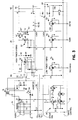
- Figure 1 is a block diagram of the circuitry associated with the constant charge time system of the present invention.
- Figure 2 is a schematic diagram of the inverter circuitry of the constant charge time system of the present invention.
- Figure 3 is a detailed schematic diagram of a portion of the circuitry illustrated in Figure 1.
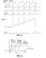
- Figure 4 illustrates the timing of various signals in the constant charge time system of the present invention.
- Figure 5 illustrates a comparison of the current in the primary of the transformer when the battery is at full charge, average charge, and depleted charge.
- Referring first to Figure 1, the constant charge time system of the present invention is generally shown at 10. The primary purpose of the
system 10 is to charge the defibrillation capacitors C1 and C2 by way of thebattery 12. While two capacitors are shown, it is possible to employ the present invention for charging one or more than two capacitors. Specifically, it is desirable to charge the capacitors C1 and C2 at a substantially constant rate over the entire life of thebattery 12. - In this regard, an
inverter circuit 14 andtransformer 16 are provided between thebattery 12 and the capacitors C1 and C2. Theinverter 14 is driven by aninverter drive circuit 18 formed as part of a lowpower hybrid circuit 20. As will be described in more detail hereinafter, theinverter 14 essentially comprises a transistor switch which is repeatedly triggered to supply power from thebattery 12 to a primary of thetransformer 16. A secondary of thetransformer 16 is charged by the primary which in turn charges the capacitors C1 and C2. - The drive frequency of the
inverter 14 is controlled by theinverter drive circuit 18. In turn, theinverter drive circuit 18 is directly controlled by the I/O control circuit 22 via themicroprocessor 24. The I/O control circuit 22 monitors, among other things, the voltage level on the defibrillation capacitors C1 and C2 to terminate the delivery of an inverter drive signal from the drive circuit to theinverter 14, when the microprocessor programmed charge on C1 and C2 has been reached. - The high
power hybrid circuit 26 is provided to gate the voltage charged on the defibrillation capacitors C1 and C2 to the defibrillation electrodes shown at 28.Microprocessor 24 is responsive to parameters related to cardiac activity for controlling the high power hybrid to pass the capacitor voltage to thedefibrillation electrodes 28. - Turning now to Figure 2, the
inverter 14,high power hybrid 26, and I/O control unit 22 are shown in more detail in connection with the defibrillation capacitors C1 and C2. Theinverter drive 18, still shown in block form, is connected between the I/O control unit 22 and theinverter unit 14. Generally, theinverter 14 comprises a FET transistor Q1, which may be, for example, model No. MTP10NIOM sold by Motorola Corporation. Theinverter drive 18 controls the state of the transistor Q1 for selectively supplying current through the drain D of the transistor Q1 to the primary 16a of thetransformer 16. Specifically, theinverter drive 18 supplies pulses in the form of an inverter drive signal at a preset frequency F to the gate G of the transistor Q1 to turn the transistor Q1 on. In an ON state, the transistor Q1 supplies current to the primary 16a while in an OFF state, no current is supplied to the primary 16a. A pulse supplied by theinverter drive 18 is terminated when the current in the mirror resistor R1 reaches a preset value. - The current in the mirror resistor R1 which is connected to the source of the transistor Q1 is fed to the I/
O control unit 22 so that it may be continuously compared with a preset value. In this regard, the I/O control unit 22 includes acomparison amplifier 32, acurrent source 34, and resistor Rd connected to a source of -6 volts. The current sensed from the mirror resistor R1 is connected to one terminal of theamplifier 32 and the other terminal of the amplifier senses voltage (VUPREF) from the node between thecurrent source 34 and divider resistor Rd. -
Inverter 14 also includes rectifier diodes D1 and D2 to ensure that current built up in the secondary 16b of thetransformer 16 charges the capacitors C1 and C2 to generate a voltage which is positive at the node VC with respect to the ground terminal connected to one terminal of the capacitor C2. - The high
power hybrid circuit 26 includes, among other sub-circuits not shown in Figure 2, two resistors R2 and R3 andswitch 42. Resistor R2 is of a substantially large value, such as 10 M ohms while resistor R2 is of a substantially small value, and can be trimmed to achieve an accurate ratio between R2 and R3. Resistor R3 is connected to a -3 volt source at one terminal thereof. The voltage between resistors R2 and R3 is tapped and fed to the I/O control circuit 22 vialine 36. The voltage online 34 is the voltage across the capacitors C1 and C2 and is termed CV. I/O control unit 22 includes acomparison amplifier 38, acurrent source 40 and resistor Rd. The line carrying the signal CV is connected to one input of thecomparator 38 and the other input terminal of thecomparator 38 is connected between thecurrent source 40 and the resistor Rd. - The output signals of
comparators microprocessor 24 for further processing as will be explained in more detail hereinafter. Generally, however, themicroprocessor 24 will cause theinverter drive 18, via I/0control circuit 22, to stop delivering drive pulses to theinverter 14 once the voltage on the defibrillation capacitors has reached the value programmed by the microprocessor by monitoring the signal CV. This is done via the DRIVE CONTROL signal shown in Figure 2. - When it is desired to discharge the voltage stored on the defibrillation capacitors C1 and C2, the microprocessor generates a signal which closes the
switch 42 in the highpower hybrid circuit 26. Onceswitch 42 is closed, the voltage across the defibrillation capacitors is supplied to one of the defibrillation electrodes 28a and 28b against the other so that an electric field is generated throughout the heart between the electrodes 28a and 28b. - Figure 3 illustrates the
inverter 14,inverter drive 18 andhigh power hybrid 26 in more detail. (Thelow power hybrid 20 is shown without the I/O control circuit 22 in Figure 3 for simplicity.) The battery is represented as VB and is connected to the source of the transistor Q1 and to theinverter drive 18. The gate of transistor Q1 requires 10 volts or more to ensure low on resistance characteristics. Because the drive signal supplied by I/O control 22 can go as low as 3 volts under transient conditions, a gate boost circuit is necessary. In this regard, theinverter drive 18 comprises transistors Q3 and Q4 which are connected so as to form a complimentary inverter for the drive signal. Capacitor C3 and diode D3 form a polarity inverter. Diode D4 and inductor L1 are connected in series with transistor Q5 and form a LC voltage doubler with the gate to source capacitance of Q1. - Under control of the DRIVE CONTROL signal, whenever transistor Q4 is turned on, capacitor C3 is charged to the supply voltage. On the other hand, when Q4 is turned off and Q3 is turned on, the polarity of capacitor C3 is reversed and the drain of Q4 is grounded. Consequently, the inverted (positive rather than negative) supply voltage is applied to the source of transistor Q5 to turn this transistor on. The combination of diode D3 and inductor L1 guarantee that the gate of transistor Q1 is driven positive with respect to the source at least three times the value of the supply voltage because the source is at a negative potential.
- As shown in Figure 3, the
inverter 14 further includes capacitors C4 and C5 which together with the inductor L3 form a filter to prevent high frequency current from flowing into the battery. Transistor Q6 is connected across the gate of transistor Q1 and together with diode D5 ensure that the actual gate voltage does not exceed 10 volts with respect to ground so that the gate of the transistor Q1 is protected when the battery is fresh (at full capacity). Transistor Q2 returns the gate of transistor Q1 to VB to ensure that it turns off quickly. - The
transformer 16 is a flyback transformer sized to allow operation at a constant charge time over a wide supply range. The charge time is chosen to be approximately 10 seconds with a new battery which is assumed to put out 6.4 volts under no load. The required inductance of the primary may be derived according to the charge time chosen for maximum battery output. It has been found that the required primary inductance is 10 microhenries. The smallest possible core for the application of this transformer is an RM4 core preferably formed of TDK H7C1 material which has a Bsat of 4000 gauss at 40 degrees Celsius. - The secondary circuit of the
transformer 16 and the capacitors C1 and C2 are charged in parallel even though they are connected in series with respect to theswitch 42 of thehigh power hybrid 26. As a result, there is no need to "balance" the capacitors to provide even voltage distribution. When the capacitors are discharged, diodes D7 and D8 insure that the larger of the two capacitors does not reverse the polarity of the smaller capacitor. - The high
power hybrid circuit 26 is designed to convey the charge on the capacitors C1 and C2 to the defibrillation electrodes 28a and 28b when the microprocessor issues a defibrillation control signal.Discharge sub-circuit 50 includes a transistor Q7 and resistor R5 which form a discharge path for the stored energy on the capacitors C1 and C2 in the event that it is necessary to charge the capacitors without delivering a pulse to the patient. Sub-circuit 50 includes an SCR Q7 and associated biasing resistor and diode (not labelled) that discharges capacitors C1 and C2 internally if therapy is not required. This is achieved by triggering the SCR Q7 to discharge the capacitors C1 and C2 through resistor R5. Terminate sub-circuit 52 includes an SCR Q8 (and associated biasing diode and resistor) for truncating the defibrillation pulse delivered to the patient by discharging the capacitors C1 and C2 directly to ground. Sub-circuits 50 and 52 are controlled by thelow power hybrid 20 as will be explained hereinafter. Resistor R6 limits the discharge current to prevent internal damage. - The
switch 42 is embodied as a silicon rectifier Q9, the gate of which is connected to transformer T2. Transformer T2 is provided for firing the SCR Q9. - As aforementioned, the voltage across the capacitors C1 and C2 is sensed through resistors R2 and R3. Diode D9 is provided to protect the system circuits in the event that R3 opens. A negative 3 volt reference is applied to the resistor R3 which is the same as that used as a reference to the
comparator 38 via resistor Rd (Figure 2). Thus, both inputs tocomparator 38 are (indirectly) referenced to negative 3 volts to allowcurrent source 40 to be programmed to zero while the comparator still has headroom for operation. - The low
power hybrid circuit 20 further includes adischarge driver circuit 54, a terminatedriver circuit 56, adefibrillation trigger circuit 58 and afault detection circuit 60. Thedischarge driver circuit 54 comprises transistor Q10 and capacitor C8 (together with associated biasing circuit elements). By bringing a signal on the line labelled DISCHARGE low, the SCR Q7 of thedischarge circuit 50 is grounded so that the charge on the capacitors C1 and C2 will be diverted through resistor R5 and SCR Q7 of the discharge sub-circuit 50 to ground. - The
defibrillation trigger circuit 58 and the terminatedriver circuit 56 are used to deliver a defibrillation or cardioversion pulse. The terminatedriver circuit 56 comprises a transistor Q11 (and associated gate drive circuit components) which is connected via a capacitor C9 to the terminate sub-circuit 52 in thehigh power hybrid 26. Similarly,defibrillation trigger circuit 58 comprises a transistor Q12 (and associated gate drive circuit components) which is connected via capacitor C10 to the transformer T2. - When the
microprocessor 24 determines that it is necessary to deliver a defibrillation or cardioversion pulse, the signal on the DEFIB line is pulled low. This turns transistor Q12 ON which discharges capacitor C10 through the pulse transformer T2. As a result, SCR Q9 is turned on and the charge on the capacitors C1 and C2 is delivered to the defibrillation electrodes vialines O circuit 22. The microprocessor responds by generating a signal on the TERM line to turn ON transistor Q11. This discharges capacitor C9 through the gate of transistor Q8 which shorts the capacitors C1 and C2 to ground through resistor R6 (approximately 2 ohms). - The
fault detection circuit 60 comprises transistor Q13, the emitter of which is connected to a resistor-diode combination R10-D7. Thefault detection circuit 60 is connected to theoutput line 64 in thehigh power hybrid 26 via resistor R11. In the event that thetransistor embodying switch 42 becomes shorted, the output of the charging current would flow through the heart. However, some of this current would also flow through resistor R11 and the emitter-base junction of transistor Q13 bringing the signal of the FAULT line high. The microprocessor senses the status on the FAULT line through the I/O control circuit 22 and shuts down theinverter 14 at once ifswitch 42 shorts. - The operation of the constant charge time mechanism will now be described with reference to Figures 2, 3 and 4. Generally, the constant charge time mechanism operates by charging the capacitors C1 and C2 in increments by repeatedly charging the primary of the
transformer 16 to a peak current value. As the battery supply voltage VB decreases, the primary current takes longer to reach the peak value. However, the drive waveform is turned off by circuitry which senses the current through the mirror resistor R1. Therefore, the peak current in the primary will remain constant regardless of the supply voltage. - The inverter drive signal generated by the
inverter drive circuit 18 under control of the microprocessor is supplied to the gate of transistor Q1. The amplitude of the inverter drive signal must be approximately 10 volts to drive the gate of the transistor Q1. In response to the 10 volt pulse of the inverter drive signal, a current is generated in the primary of thetransformer 16. The level of the current IPRI in the primary is sensed via the mirror resistor R1 and reflected as a voltage hereinafter referred to as OVER I. The current in the mirror resistor is a known fraction (1/1000) of the current in the primary of thetransformer 16. OVER I is compared in thecomparator amplifier 32 with a preset reference level ISET of 0.4 V. - Once the OVER I voltage reaches the preset reference level, the microprocessor terminates the positive portion of the inverter drive signal via the DRIVE CONTROL signal. The current in the secondary of the transformer ISEC jumps to a maximum value at the maximum of the current in the primary, and then begins to decay. As a result, the voltage VC across the capacitors C1 and C2 rises in response to the current in the secondary of the transformer. However, once the current in the secondary returns to zero, the voltage across the capacitors stops rising. The signal CV representing the capacitor voltage is constantly monitored in the I/
O control 22 and compared with the programmed final voltage level of the capacitors, hereinafter referred to as VUPREF. At the next occurrence of a positive pulse in the inverter drive signal, the mechanism repeats and the voltage across the capacitors C1 and C2 (VC) rises from the previously charged level to a higher level. When the voltage across the capacitors reaches the final level set by VUPREF, thecomparator 38 issues a pulse as shown in Figure 4 which is detected by the microprocessor to terminate the DRIVE signal. The level of VUPREF is programmable (via the current source 40) from 0 to 2.4 volts (DC) (or -3 volts to -0.6 volts with respect to the -3 volt reference) creating an energy output of 0.1 to 34 Joules. - The energy stored in the primary of the transformer each cycle of the drive signal is equal to 1/2LIPK where L is the inductance of the primary 16a of the
transformer 16. Assuming ideal conditions with ideal inductors and zero ohm switches, the on-time tON is equal to IPKL/VBAT so that IPK is equal to VBATtON/L. If the frequency of the drive signal is maintained constant, then the energy delivered to the capacitors per cycle is constant, the result being that the charge time of the capacitors is constant. The value tON in the foregoing equations represents the time needed for the current in the primary (IPRI) to reach IPK. Particularly, because the capacitor is charged in increments (Figure 4), the total time to charge the capacitors is the sum of the charge time for the charging increments. Thus, by ensuring that the current in the primary of the transformer reaches a peak level within a constant period of time, the charging increments are effected in a constant period of time. In effect, the battery power supply is intermittently connected to the capacitor at a fixed frequency. - Shown in Figure 5 is a comparison of the current in the primary 16a of the
transformer 16 at three different approximate battery voltages. When the battery is new and thus at high voltages, the current in the primary will reach the peak value more quickly than when the battery voltage is at an average level or a depleted low level. As aforementioned, however, the inverter drive signal is terminated according to the current through the mirror resistor R1 via the DRIVE CONTROL signal from themicroprocessor 24. Thus the peak current will remain constant regardless of battery voltage. - The above description is intended by way of example only and is not intended to limit the present invention in any way except as set forth in the following claims.
Claims (11)
- A capacitor charging circuit for charging a defibrillation capacitor comprising:
battery supply means for providing a supply voltage;
defibrillation capacitor means for being charged to a predetermined voltage;
transformer means comprising a primary and a secondary, the secondary being connected to said defibrillation capacitor means, the secondary being charged by said primary for delivering current to the defibrillation capacitor means;
inverter means connected to said battery supply means and to the primary of said transformer means, said inverter means capable of assuming a first state in which current is supplied from the battery supply means to the primary of the transformer means and a second state in which no current is supplied to the primary;
inverter drive means connected to the inverter means for generating an inverter drive signal comprising repeating spaced pulses, each pulse of the inverter drive signal triggering the inverter means to assume said first state to supply current to the primary of the transformer means for a duration corresponding to a duration of each pulse; and
control means connected to said defibrillation capacitor means, to said inverter means and to said inverter drive means, said control means monitoring the voltage across said defibrillation capacitor means and monitoring the current in the primary of the transformer means to terminate each pulse of the inverter drive signal in response to the current in the primary reaching a preset value, and to terminate the inverter drive signal in response to the voltage of said defibrillation capacitor means reaching said predetermined voltage, said control means controlling said inverter drive means to maintain the frequency of the inverter drive signal constant so that the energy delivered to the defibrillation capacitor means from the secondary of the transformer means per cycle of the inverter drive signal is constant. - The capacitor charging circuit of claim 1, wherein the inverter means comprises an FET transistor having a gate connected to said inverter drive means to receive said inverter drive signal, a drain connected to said primary of the transformer means and a source.
- The capacitor charging circuit of claim 2, and further comprising a mirror resistor connected to the source of the FET transistor, the current in the mirror resistor being a fraction of the current in the primary of the transformer means.
- The capacitor charging circuit of claim 3, wherein said control means monitors the current in the primary of the transformer means by monitoring the current in the mirror resistor.
- The capacitor charging circuit of claim 4, wherein said control means comprises a first comparator for comparing the current in the mirror resistor with said preset value and a second comparator for comparing the voltage across the defibrillation capacitor means with said predetermined voltage.
- The capacitor charging circuit of claim 4, wherein said defibrillation capacitor means comprises first and second capacitors connected in series.
- The capacitor charging circuit of claim 1, wherein said inverter means charges the primary of the transformer means in response to each pulse of the inverter drive signal so that the secondary of the transformer means supplies current to the defibrillation capacitor means during an off half cycle of the inverter drive signal when no pulse is present, the charge being built up in the defibrillation capacitor means incrementally during the off half cycle of the inverter drive signal until the predetermined voltage is reached.
- A system for controlling the charging and discharging of a defibrillation capacitor comprising:
battery supply means for providing a supply voltage;
defibrillation capacitor means for being charged to a predetermined voltage;
transformer means comprising a primary and a secondary, the secondary being connected to said defibrillation capacitor means, the secondary being charged by said primary for delivering current to the defibrillation capacitor means;
inverter means connected to said battery supply means and to the primary of said transformer means, said inverter means capable of assuming a first state in which current is supplied from the battery supply means to the primary of the transformer means and a second state in which no current is supplied to the primary;
inverter drive means connected to the inverter means for generating an inverter drive signal comprising repeating spaced pulses, each pulse of the drive signal triggering the inverter means to assume said first state to supply current to the primary of the transformer means for a duration corresponding to a duration of each pulse;
control means connected to said defibrillation capacitor means, to said inverter means and to said inverter drive means, said control means monitoring the voltage across said defibrillation capacitor means and monitoring the current in the primary of the transformer means to terminate each pulse of the inverter drive signal in response to the current in the primary reaching a preset value, and to terminate the inverter drive signal in response to the voltage of said defibrillation capacitor means reaching said predetermined voltage, said control means controlling said inverter drive means to maintain the frequency of the inverter drive signal constant so that the energy delivered to the defibrillation capacitor means from the secondary of the transformer means per cycle of the inverter drive signal is constant;
defibrillation trigger means connected to said defibrillation capacitor means for triggering the discharge of said defibrillation capacitor means to defibrillation electrodes;
termination means connected to said defibrillation capacitor means for terminating the discharge of said defibrillation capacitor means a preset period of time after the discharge of the defibrillation capacitor means to the defibrillation electrodes by directing the charge of said defibrillation capacitor means to ground; and
internal discharge means for connecting the defibrillation capacitor means to ground upon desiring not to deliver a defibrillation shock. - The system of claim 8, wherein said inverter means charges the primary of the transformer means in response to each pulse of the inverter drive signal so that the secondary of the transformer means supplies current to the defibrillation capacitor means during an off half cycle of the inverter drive signal when no pulse is present, the charge being built up in the defibrillation capacitor means incrementally during the off half cycle of the inverter drive signal until the predetermined voltage is reached.
- A method for charging a defibrillation capacitor comprising the steps of:(a) providing a supply voltage;(b) supplying current to a primary of a transformer during a first half cycle from said supply voltage;(c) charging a defibrillation capacitor from a secondary of the transformer during a second half cycle;(d) monitoring the level of the current in the primary of the transformer and repeating steps (b)-(c) at a constant frequency equal to the inverse of the sum of the first and second half cycles, until the current in the primary of the transformer reaches a preset value; and(e) monitoring the voltage across the defibrillation capacitor and repeating steps (b)-(d) until the voltage across the defibrillation capacitor accumulates and reaches a preset value and so that the energy delivered to the defibrillation capacitor per a full cycle comprising the sum of the first and second half-cycles, is constant.
- A method for charging a defibrillation capacitor comprising the steps of:
providing a supply voltage;
intermittently connecting the supply voltage to a defibrillation capacitor at a fixed frequency for a period of time during which current is supplied to said defibrillation capacitor;
monitoring accumulation of voltage across the defibrillation capacitor as a result of said step of intermittent connection;
terminating the intermittent connection of the supply voltage to the defibrillation capacitor upon the voltage across the defibrillation capacitor reaching a preset value whereby a constant amount of energy is supplied to the defibrillation capacitor per a connection cycle of said defibrillation capacitor to said supply voltage.
Applications Claiming Priority (2)
| Application Number | Priority Date | Filing Date | Title |
|---|---|---|---|
| US97854992A | 1992-11-19 | 1992-11-19 | |
| US978549 | 1992-11-19 |
Publications (3)
| Publication Number | Publication Date |
|---|---|
| EP0598225A2 true EP0598225A2 (en) | 1994-05-25 |
| EP0598225A3 EP0598225A3 (en) | 1998-02-25 |
| EP0598225B1 EP0598225B1 (en) | 2001-01-03 |
Family
ID=25526200
Family Applications (1)
| Application Number | Title | Priority Date | Filing Date |
|---|---|---|---|
| EP93116707A Expired - Lifetime EP0598225B1 (en) | 1992-11-19 | 1993-10-15 | System for constant charge time of a defibrillation capacitor and for its discharge |
Country Status (7)
| Country | Link |
|---|---|
| US (1) | US5800461A (en) |
| EP (1) | EP0598225B1 (en) |
| JP (1) | JP2825748B2 (en) |
| AT (1) | ATE198425T1 (en) |
| AU (1) | AU659569B2 (en) |
| CA (1) | CA2103405C (en) |
| DE (1) | DE69329816T2 (en) |
Cited By (4)
| Publication number | Priority date | Publication date | Assignee | Title |
|---|---|---|---|---|
| US5545181A (en) * | 1993-10-15 | 1996-08-13 | Ela Medical, S.A. | Implantable defibrillator/pacer using negative voltage supplies |
| GB2303229A (en) * | 1995-03-30 | 1997-02-12 | Eddie Palin Distribution Limit | Constant power output circuit for an electric fence |
| EP0916365A1 (en) * | 1997-11-14 | 1999-05-19 | Marquette Hellige GmbH | Defibrillator with improved use of the battery energy |
| CN107050642A (en) * | 2016-12-03 | 2017-08-18 | 潍坊大地医疗器械有限公司 | A kind of electronic channel therapeutic equipment for preventing that electric current is excessive |
Families Citing this family (16)
| Publication number | Priority date | Publication date | Assignee | Title |
|---|---|---|---|---|
| US5879374A (en) * | 1993-05-18 | 1999-03-09 | Heartstream, Inc. | External defibrillator with automatic self-testing prior to use |
| US6076018A (en) * | 1998-09-04 | 2000-06-13 | Woodside Biomedical, Inc | Method and apparatus for low power regulated output in battery powered electrotherapy devices |
| US6243604B1 (en) | 1999-02-26 | 2001-06-05 | Medical Research Laboratories, Inc. | Apparatus for charging defibrillator capacitors |
| US6839590B2 (en) | 2001-10-22 | 2005-01-04 | Medtronic Physio-Control Corp. | Average current mode controlled energy storage in a defibrillator |
| US20040064157A1 (en) * | 2002-09-30 | 2004-04-01 | Norton John D. | Method and apparatus for maintaining energy storage in an electrical storage device |
| US7212856B2 (en) * | 2003-07-29 | 2007-05-01 | Medtronic, Inc. | Reformation techniques for capacitors of implantable medical devices |
| US7602597B2 (en) * | 2003-10-07 | 2009-10-13 | Taser International, Inc. | Systems and methods for immobilization using charge delivery |
| US7151962B2 (en) * | 2004-04-29 | 2006-12-19 | Medtronic, Inc. | Method and apparatus to control delivery of high-voltage and anti-tachy pacing therapy in an implantable medical device |
| US7986506B2 (en) * | 2006-05-03 | 2011-07-26 | Taser International, Inc. | Systems and methods for arc energy regulation and pulse delivery |
| EP2229214B1 (en) | 2007-12-13 | 2016-07-27 | Cardiac Pacemakers, Inc. | Defibrillation shock output circuit |
| US8433404B2 (en) * | 2009-05-19 | 2013-04-30 | Cardiac Pacemakers, Inc. | Integrated high voltage output circuit |
| US9126055B2 (en) | 2012-04-20 | 2015-09-08 | Cardiac Science Corporation | AED faster time to shock method and device |
| CN102631749B (en) * | 2012-04-25 | 2014-12-10 | 王吉云 | External defibrillation circuit |
| US9435142B2 (en) | 2014-02-28 | 2016-09-06 | Schlage Lock Company Llc | Method of operating an access control system |
| CN110520190A (en) | 2017-04-27 | 2019-11-29 | 维曼急救医疗科技两合公司 | Method and apparatus for defibrillation |
| US10033285B1 (en) * | 2017-06-19 | 2018-07-24 | Dialog Semiconductor Inc. | Secondary controller for a flyback converter including a sense resistor fault detection |
Family Cites Families (36)
| Publication number | Priority date | Publication date | Assignee | Title |
|---|---|---|---|---|
| US3226630A (en) * | 1963-03-01 | 1965-12-28 | Raytheon Co | Power supply regulators |
| US3383584A (en) * | 1965-03-16 | 1968-05-14 | Navy Usa | Solid state switching regulator circuit |
| US3376489A (en) * | 1966-02-21 | 1968-04-02 | Caterpillar Tractor Co | Regulated power supply |
| US3746005A (en) * | 1968-04-11 | 1973-07-17 | American Optical Corp | Constant energy heartbeat stimulating apparatus with pulse width control |
| US3759265A (en) * | 1968-04-11 | 1973-09-18 | American Optical Corp | Tem pulse width controlled heartbeat stimulating apparatus monitoring sys |
| US3547127A (en) * | 1968-04-29 | 1970-12-15 | Medtronic Inc | Cardiac pacemaker with regulated power supply |
| US3757795A (en) * | 1968-10-28 | 1973-09-11 | Medtronic Inc | Power supply and voltage double output circuitry for implantable electro-medical apparatus |
| US3746006A (en) * | 1971-07-15 | 1973-07-17 | American Optical Corp | Controlled energy output pacer |
| US3782389A (en) * | 1972-01-20 | 1974-01-01 | Health Technology Labs Inc | Computer controlled defibrillator |
| US3867949A (en) * | 1973-04-27 | 1975-02-25 | Cardiac Pacemakers Inc | Cardiac pacer with voltage doubler output circuit |
| US3835368A (en) * | 1973-05-21 | 1974-09-10 | Gen Electric | Voltage regulator for a direct current power supply |
| US3860864A (en) * | 1973-09-17 | 1975-01-14 | Marconi Co Ltd | Power supply circuits |
| US4056105A (en) * | 1974-11-19 | 1977-11-01 | Westinghouse Electric Corporation | Pulse generator |
| US4015609A (en) * | 1975-11-17 | 1977-04-05 | Vitatron Medical B.V. | Circuit for low power-low energy source |
| US4120306A (en) * | 1976-01-22 | 1978-10-17 | Vitatron Medical B.V. | Cardiac pacer with pre-programmed power source interface means |
| US4345604A (en) * | 1976-01-22 | 1982-08-24 | Vitafin N.V. | Long life cardiac pacer with switching power |
| US4345606A (en) * | 1977-12-13 | 1982-08-24 | Littleford Philip O | Split sleeve introducers for pacemaker electrodes and the like |
| US4119903A (en) * | 1978-01-05 | 1978-10-10 | Hewlett-Packard Company | Defibrillator charging circuit |
| US4233659A (en) * | 1978-01-05 | 1980-11-11 | Hewlett-Packard Company | Defibrillator charging current regulator |
| SU1000030A1 (en) * | 1980-02-28 | 1983-02-28 | Научно-Производственное Объединение По Радиоэлектронной Медицинской Аппаратуре "Рэма" | Defibriller |
| US4590941A (en) * | 1981-03-02 | 1986-05-27 | Cordis Corporation | Cardiac pacer with improved battery system, output circuitry, and emergency operation |
| US4437466A (en) * | 1981-03-02 | 1984-03-20 | Cordis Corporation | Cardiac pacer with improved battery system, output circuitry, and emergency operation |
| US4488555A (en) * | 1982-12-13 | 1984-12-18 | Mieczyslaw Mirowski | Battery condition warning system for medical implant |
| US4489369A (en) * | 1983-06-28 | 1984-12-18 | The United States Of America As Represented By The Secretary Of The Navy | Control circuit for a flyback stepcharger |
| US4548209A (en) * | 1984-02-06 | 1985-10-22 | Medtronic, Inc. | Energy converter for implantable cardioverter |
| US4595009A (en) * | 1984-02-06 | 1986-06-17 | Medtronic, Inc. | Protection circuit for implantable cardioverter |
| US4599523A (en) * | 1984-02-16 | 1986-07-08 | Intermedics, Inc. | Power priority system |
| US4586118A (en) * | 1984-06-05 | 1986-04-29 | The United States Of America As Represented By The United States Department Of Energy | Capacitor charging FET switcher with controller to adjust pulse width |
| US4599554A (en) * | 1984-12-10 | 1986-07-08 | Texet Corportion | Vertical MOSFET with current monitor utilizing common drain current mirror |
| US4800883A (en) * | 1986-04-02 | 1989-01-31 | Intermedics, Inc. | Apparatus for generating multiphasic defibrillation pulse waveform |
| US4823796A (en) * | 1987-04-03 | 1989-04-25 | Laerdal Manufacturing Corp. | Defibrillator circuit for producing a trapezoidal defibrillation pulse |
| JPH0336546A (en) * | 1989-07-03 | 1991-02-18 | Konica Corp | Storage method for photosensitive printing plate |
| US5097830A (en) * | 1990-03-30 | 1992-03-24 | Laerdal Manufacturing Corporation | Defibrillator with reliability verification |
| FR2662557B1 (en) * | 1990-05-22 | 1997-07-25 | Thomson Brandt Armements | LOW VOLTAGE TO HIGH VOLTAGE CONVERTER. |
| US5163428A (en) * | 1990-10-11 | 1992-11-17 | Ventritex, Inc. | Implantable cardiac defibrillator with current leakage detecting means |
| US5237989A (en) * | 1991-04-04 | 1993-08-24 | Physio-Control Corporation | Cardiac defibrillator with movable contact switch |
-
1993
- 1993-10-15 EP EP93116707A patent/EP0598225B1/en not_active Expired - Lifetime
- 1993-10-15 AT AT93116707T patent/ATE198425T1/en not_active IP Right Cessation
- 1993-10-15 DE DE69329816T patent/DE69329816T2/en not_active Expired - Fee Related
- 1993-10-22 AU AU49189/93A patent/AU659569B2/en not_active Ceased
- 1993-11-18 CA CA002103405A patent/CA2103405C/en not_active Expired - Fee Related
- 1993-11-19 JP JP5290689A patent/JP2825748B2/en not_active Expired - Fee Related
-
1995
- 1995-11-13 US US08/538,831 patent/US5800461A/en not_active Expired - Fee Related
Non-Patent Citations (1)
| Title |
|---|
| None |
Cited By (6)
| Publication number | Priority date | Publication date | Assignee | Title |
|---|---|---|---|---|
| US5545181A (en) * | 1993-10-15 | 1996-08-13 | Ela Medical, S.A. | Implantable defibrillator/pacer using negative voltage supplies |
| GB2303229A (en) * | 1995-03-30 | 1997-02-12 | Eddie Palin Distribution Limit | Constant power output circuit for an electric fence |
| GB2303229B (en) * | 1995-03-30 | 1999-06-02 | Eddie Palin Distribution Limit | Constant power output circuit |
| EP0916365A1 (en) * | 1997-11-14 | 1999-05-19 | Marquette Hellige GmbH | Defibrillator with improved use of the battery energy |
| US6070099A (en) * | 1997-11-14 | 2000-05-30 | Marquette Medical Gmbh | Defibrillator with improved utilization of the accumulator energy |
| CN107050642A (en) * | 2016-12-03 | 2017-08-18 | 潍坊大地医疗器械有限公司 | A kind of electronic channel therapeutic equipment for preventing that electric current is excessive |
Also Published As
| Publication number | Publication date |
|---|---|
| CA2103405A1 (en) | 1994-05-20 |
| JPH06339535A (en) | 1994-12-13 |
| US5800461A (en) | 1998-09-01 |
| ATE198425T1 (en) | 2001-01-15 |
| CA2103405C (en) | 2000-01-25 |
| AU4918993A (en) | 1994-06-02 |
| DE69329816D1 (en) | 2001-02-08 |
| EP0598225A3 (en) | 1998-02-25 |
| EP0598225B1 (en) | 2001-01-03 |
| DE69329816T2 (en) | 2001-04-19 |
| JP2825748B2 (en) | 1998-11-18 |
| AU659569B2 (en) | 1995-05-18 |
Similar Documents
| Publication | Publication Date | Title |
|---|---|---|
| US5800461A (en) | Constant charge time of defibrillation capacitor | |
| US5178140A (en) | Implantable medical devices employing capacitive control of high voltage switches | |
| US6980856B2 (en) | Circuit for performing external pacing and biphasic defibrillation | |
| US4399818A (en) | Direct-coupled output stage for rapid-signal biological stimulator | |
| EP0588126B1 (en) | Implantable heart defibrillator | |
| US20230077540A1 (en) | Method and apparatus for applying a rectilinear biphasic power waveform to a load | |
| US4800883A (en) | Apparatus for generating multiphasic defibrillation pulse waveform | |
| US4693253A (en) | Automatic implantable defibrillator and pacer | |
| US5407444A (en) | Staged energy concentration for a defibrillator | |
| USRE38777E1 (en) | Dual battery power system for an implantable cardioverter defibrillator with voltage booster | |
| US5447522A (en) | Capacitor charging circuit for implantable defibrillator | |
| US6175765B1 (en) | H-bridge circuit for generating a high-energy biphasic waveform in an external defibrillator | |
| US6097982A (en) | Patient-worn energy delivery apparatus | |
| US4595009A (en) | Protection circuit for implantable cardioverter | |
| US5111816A (en) | System configuration for combined defibrillator/pacemaker | |
| US5824017A (en) | H-bridge circuit for generating a high-energy biphasic waveform in an external defibrillator | |
| US5265588A (en) | VCO driven flyback converter for implantable cardoverter/defibrillator | |
| US5601610A (en) | Current leakage prevention circuit for an external defibrillator | |
| US20030216786A1 (en) | Circuit for producing an arbitrary defibrillation waveform | |
| US6546287B1 (en) | Controlled-power defibrillator and method of defibrillation | |
| US6968230B2 (en) | H-bridge circuit for generating a high-energy biphasic and external pacing waveform in an external defibrillator | |
| US5545181A (en) | Implantable defibrillator/pacer using negative voltage supplies | |
| US6035235A (en) | Amplified voltage output switching network for a self-powered defibrillator | |
| US5745350A (en) | Power supply circuit with a widely varying input voltage | |
| US6839590B2 (en) | Average current mode controlled energy storage in a defibrillator |
Legal Events
| Date | Code | Title | Description |
|---|---|---|---|
| PUAI | Public reference made under article 153(3) epc to a published international application that has entered the european phase |
Free format text: ORIGINAL CODE: 0009012 |
|
| AK | Designated contracting states |
Kind code of ref document: A2 Designated state(s): AT BE CH DE DK ES FR GB GR IE IT LI LU MC NL PT SE |
|
| PUAL | Search report despatched |
Free format text: ORIGINAL CODE: 0009013 |
|
| AK | Designated contracting states |
Kind code of ref document: A3 Designated state(s): AT BE CH DE DK ES FR GB GR IE IT LI LU MC NL PT SE |
|
| 17P | Request for examination filed |
Effective date: 19980518 |
|
| 17Q | First examination report despatched |
Effective date: 19981130 |
|
| GRAG | Despatch of communication of intention to grant |
Free format text: ORIGINAL CODE: EPIDOS AGRA |
|
| RTI1 | Title (correction) |
Free format text: SYSTEM FOR CONSTANT CHARGE TIME OF A DEFIBRILLATION CAPACITOR AND FOR ITS DISCHARGE |
|
| RTI1 | Title (correction) |
Free format text: SYSTEM FOR CONSTANT CHARGE TIME OF A DEFIBRILLATION CAPACITOR AND FOR ITS DISCHARGE |
|
| GRAG | Despatch of communication of intention to grant |
Free format text: ORIGINAL CODE: EPIDOS AGRA |
|
| GRAH | Despatch of communication of intention to grant a patent |
Free format text: ORIGINAL CODE: EPIDOS IGRA |
|
| GRAH | Despatch of communication of intention to grant a patent |
Free format text: ORIGINAL CODE: EPIDOS IGRA |
|
| GRAA | (expected) grant |
Free format text: ORIGINAL CODE: 0009210 |
|
| AK | Designated contracting states |
Kind code of ref document: B1 Designated state(s): AT BE CH DE DK ES FR GB GR IE IT LI LU MC NL PT SE |
|
| PG25 | Lapsed in a contracting state [announced via postgrant information from national office to epo] |
Ref country code: SE Free format text: LAPSE BECAUSE OF FAILURE TO SUBMIT A TRANSLATION OF THE DESCRIPTION OR TO PAY THE FEE WITHIN THE PRESCRIBED TIME-LIMIT Effective date: 20010103 Ref country code: GR Free format text: LAPSE BECAUSE OF NON-PAYMENT OF DUE FEES Effective date: 20010103 Ref country code: ES Free format text: THE PATENT HAS BEEN ANNULLED BY A DECISION OF A NATIONAL AUTHORITY Effective date: 20010103 |
|
| REF | Corresponds to: |
Ref document number: 198425 Country of ref document: AT Date of ref document: 20010115 Kind code of ref document: T |
|
| REG | Reference to a national code |
Ref country code: CH Ref legal event code: NV Representative=s name: PATENTANWAELTE SCHAAD, BALASS, MENZL & PARTNER AG Ref country code: CH Ref legal event code: EP |
|
| REG | Reference to a national code |
Ref country code: IE Ref legal event code: FG4D |
|
| REF | Corresponds to: |
Ref document number: 69329816 Country of ref document: DE Date of ref document: 20010208 |
|
| ITF | It: translation for a ep patent filed |
Owner name: GUZZI E RAVIZZA S.R.L. |
|
| PG25 | Lapsed in a contracting state [announced via postgrant information from national office to epo] |
Ref country code: PT Free format text: LAPSE BECAUSE OF FAILURE TO SUBMIT A TRANSLATION OF THE DESCRIPTION OR TO PAY THE FEE WITHIN THE PRESCRIBED TIME-LIMIT Effective date: 20010403 Ref country code: DK Free format text: LAPSE BECAUSE OF FAILURE TO SUBMIT A TRANSLATION OF THE DESCRIPTION OR TO PAY THE FEE WITHIN THE PRESCRIBED TIME-LIMIT Effective date: 20010403 |
|
| ET | Fr: translation filed | ||
| PG25 | Lapsed in a contracting state [announced via postgrant information from national office to epo] |
Ref country code: MC Free format text: LAPSE BECAUSE OF NON-PAYMENT OF DUE FEES Effective date: 20011015 Ref country code: LU Free format text: LAPSE BECAUSE OF NON-PAYMENT OF DUE FEES Effective date: 20011015 |
|
| PLBE | No opposition filed within time limit |
Free format text: ORIGINAL CODE: 0009261 |
|
| STAA | Information on the status of an ep patent application or granted ep patent |
Free format text: STATUS: NO OPPOSITION FILED WITHIN TIME LIMIT |
|
| REG | Reference to a national code |
Ref country code: GB Ref legal event code: IF02 |
|
| 26N | No opposition filed | ||
| PGFP | Annual fee paid to national office [announced via postgrant information from national office to epo] |
Ref country code: IE Payment date: 20050914 Year of fee payment: 13 |
|
| PGFP | Annual fee paid to national office [announced via postgrant information from national office to epo] |
Ref country code: FR Payment date: 20050916 Year of fee payment: 13 |
|
| PGFP | Annual fee paid to national office [announced via postgrant information from national office to epo] |
Ref country code: GB Payment date: 20051010 Year of fee payment: 13 |
|
| PGFP | Annual fee paid to national office [announced via postgrant information from national office to epo] |
Ref country code: BE Payment date: 20051012 Year of fee payment: 13 |
|
| PGFP | Annual fee paid to national office [announced via postgrant information from national office to epo] |
Ref country code: NL Payment date: 20051018 Year of fee payment: 13 |
|
| PGFP | Annual fee paid to national office [announced via postgrant information from national office to epo] |
Ref country code: CH Payment date: 20051021 Year of fee payment: 13 |
|
| PGFP | Annual fee paid to national office [announced via postgrant information from national office to epo] |
Ref country code: AT Payment date: 20051024 Year of fee payment: 13 |
|
| PG25 | Lapsed in a contracting state [announced via postgrant information from national office to epo] |
Ref country code: AT Free format text: LAPSE BECAUSE OF NON-PAYMENT OF DUE FEES Effective date: 20061015 |
|
| PG25 | Lapsed in a contracting state [announced via postgrant information from national office to epo] |
Ref country code: IE Free format text: LAPSE BECAUSE OF NON-PAYMENT OF DUE FEES Effective date: 20061016 |
|
| PG25 | Lapsed in a contracting state [announced via postgrant information from national office to epo] |
Ref country code: LI Free format text: LAPSE BECAUSE OF NON-PAYMENT OF DUE FEES Effective date: 20061031 Ref country code: CH Free format text: LAPSE BECAUSE OF NON-PAYMENT OF DUE FEES Effective date: 20061031 |
|
| PGFP | Annual fee paid to national office [announced via postgrant information from national office to epo] |
Ref country code: IT Payment date: 20061031 Year of fee payment: 14 |
|
| PGFP | Annual fee paid to national office [announced via postgrant information from national office to epo] |
Ref country code: DE Payment date: 20061229 Year of fee payment: 14 |
|
| PG25 | Lapsed in a contracting state [announced via postgrant information from national office to epo] |
Ref country code: NL Free format text: LAPSE BECAUSE OF NON-PAYMENT OF DUE FEES Effective date: 20070501 |
|
| REG | Reference to a national code |
Ref country code: CH Ref legal event code: PL |
|
| GBPC | Gb: european patent ceased through non-payment of renewal fee |
Effective date: 20061015 |
|
| NLV4 | Nl: lapsed or anulled due to non-payment of the annual fee |
Effective date: 20070501 |
|
| REG | Reference to a national code |
Ref country code: IE Ref legal event code: MM4A |
|
| REG | Reference to a national code |
Ref country code: FR Ref legal event code: ST Effective date: 20070629 |
|
| PG25 | Lapsed in a contracting state [announced via postgrant information from national office to epo] |
Ref country code: GB Free format text: LAPSE BECAUSE OF NON-PAYMENT OF DUE FEES Effective date: 20061015 |
|
| BERE | Be: lapsed |
Owner name: *CARDIAC PACEMAKERS INC. Effective date: 20061031 |
|
| PG25 | Lapsed in a contracting state [announced via postgrant information from national office to epo] |
Ref country code: FR Free format text: LAPSE BECAUSE OF NON-PAYMENT OF DUE FEES Effective date: 20061031 |
|
| PG25 | Lapsed in a contracting state [announced via postgrant information from national office to epo] |
Ref country code: DE Free format text: LAPSE BECAUSE OF NON-PAYMENT OF DUE FEES Effective date: 20080501 |
|
| PG25 | Lapsed in a contracting state [announced via postgrant information from national office to epo] |
Ref country code: IT Free format text: LAPSE BECAUSE OF NON-PAYMENT OF DUE FEES Effective date: 20071015 Ref country code: BE Free format text: LAPSE BECAUSE OF FAILURE TO SUBMIT A TRANSLATION OF THE DESCRIPTION OR TO PAY THE FEE WITHIN THE PRESCRIBED TIME-LIMIT Effective date: 20061031 |