EP0598112B1 - Process and configuration for establishing the sum of a chain of products - Google Patents
Process and configuration for establishing the sum of a chain of products Download PDFInfo
- Publication number
- EP0598112B1 EP0598112B1 EP93916269A EP93916269A EP0598112B1 EP 0598112 B1 EP0598112 B1 EP 0598112B1 EP 93916269 A EP93916269 A EP 93916269A EP 93916269 A EP93916269 A EP 93916269A EP 0598112 B1 EP0598112 B1 EP 0598112B1
- Authority
- EP
- European Patent Office
- Prior art keywords
- register
- product
- sum
- output
- partial sum
- Prior art date
- Legal status (The legal status is an assumption and is not a legal conclusion. Google has not performed a legal analysis and makes no representation as to the accuracy of the status listed.)
- Expired - Lifetime
Links
Images


Classifications
-
- G—PHYSICS
- G06—COMPUTING; CALCULATING OR COUNTING
- G06F—ELECTRIC DIGITAL DATA PROCESSING
- G06F7/00—Methods or arrangements for processing data by operating upon the order or content of the data handled
- G06F7/38—Methods or arrangements for performing computations using exclusively denominational number representation, e.g. using binary, ternary, decimal representation
- G06F7/48—Methods or arrangements for performing computations using exclusively denominational number representation, e.g. using binary, ternary, decimal representation using non-contact-making devices, e.g. tube, solid state device; using unspecified devices
- G06F7/544—Methods or arrangements for performing computations using exclusively denominational number representation, e.g. using binary, ternary, decimal representation using non-contact-making devices, e.g. tube, solid state device; using unspecified devices for evaluating functions by calculation
- G06F7/5443—Sum of products
Definitions
- the invention relates to a method for forming the sum a chain of products made up of two numbers one after the other are supplied, each intermediate result of the Sum formation is cached, as well as an arrangement to form the sum of a chain of products a first and a second value each, with a Storage arrangement for storing a number of values with a predetermined first number of bits, a clock-controlled Control arrangement for controlling the registered mail of values in registers, a first register arrangement for Record two each to be multiplied Values, a multiplication arrangement by two Inputs connected to the first register arrangement and a downstream product register with a Output for twice the first number of bits, an adding arrangement with two total inputs for the first number each Bits, one of which is connected to the output of the product register can be coupled, and a downstream sum register from at least two subtotals for each the first number of bits, with an output connected to the other input of the adder arrangement can be coupled.
- the object of the invention is a method of the beginning Specify the type specified, which is the formation of the sum of a Chain of products with little effort with only a little reduced Allows speed.
- This object is achieved according to claim 1 in that with each individual multiplication the resulting product is temporarily stored and in two steps are added to the interim result by first step only the digits of lowest value Product to the corresponding places in the interim result added and the resulting first partial sum is cached and in the second step the remaining digits of higher value of the product to the corresponding remaining digits of the subtotal and added to the transfer of the first subtotal and the same resulting second partial sum is buffered, in each step a different one of the immediate is then fed to multiply numbers.
- Another object of the invention is to provide a Specify an arrangement of the type mentioned that the Form the sum of a chain of products with less Effort with only a slightly reduced speed enables.
- the memory arrangement (12) is connected to the first register arrangement (16, 18) for the first number of bits via only one data bus (14) and in that the control arrangement (10) is set up to alternate to work in a first and a second cycle time and in the first cycle time to supply the first number of least significant bits at the output of the product register (22) and the content of the second partial sum register (32) to the inputs of the adder arrangement (26) and at the end of this cycle time one write the first values (B i ) into the register arrangement (16) and the new partial sum present at the output of the adding arrangement (26) into the second partial sum register (32) and in the second cycle time the first number of bits of the highest value at the output of the product register (22 ) and the content of the first partial sum register and a buffered carry of the adder arrangement (26) and at the end of this T one of the second values (A i + 1 ) into the register arrangement (16, 18) and the second partial sum present at the output of the adding arrangement (26) into the first partial sum
- Each complete partial sum is thus in two cycle times formed so that the processing speed is halved overall.
- this is just a simple one Data bus required over which to be processed Values are transferred sequentially and it is further also an adder arrangement with only the simple word width sufficient that the subtotals in the two cycle times determined one after the other. Since initially only the partial sum The bits with the lowest value are formed for the formation of the second subtotal of the carry over from the first subtotal available. This creates no rounding errors, since all existing positions are actually be evaluated while the exact result finally taken from the second partial total register can be.
- a control arrangement 10 generates two control signals T1 and T2 on lines 8 and 9, which are Alternate cyclically.
- the control arrangement 10 also generates at an output 11 addresses for addressing one Memory arrangement 12.
- the connection 11 is double here drawn as these actually consist of a number parallel lines exist over which the bits one Address can be transmitted in parallel. This also applies to the also double-drawn data connections that also actually consist of several lines, over which the bits of a data word are transmitted in parallel become.
- the data connector of the memory array 12 which is also made up of several individual memories including if necessary Read-only memories can exist with a data bus 14 connected to the other, not shown
- a processor sets up the two registers 16 and 18 are connected in parallel. Enrolling in this Register is controlled by control signals on lines 8 and 9 controlled.
- the outputs 17 and 19 of the registers 16 and 18, which for Record the factors to be multiplied together are determined with the inputs of a multiplier arrangement 20 connected, the within a cycle time complete product of the two via compounds 17 and 19 supplied values forms and the product at the exit 21 issues.
- This has twice the word width, i.e. twice the number of bits of the supplied factors. This is the only place in the order after Fig. 1, on which a double word width occurs, and the Connection 21 is with the receipt of a product register 22 connected, also for this double Word width is designed.
- each Connection On the output side there are two connections to the product register 22 23 and 29 connected, of which the connection 23 the most significant bits and the connection 29 carries the least significant bits, i.e. each Connection has the simple word width.
- the connections 23 and 29 lead to a multiplexer that over a control signal on line 8 controls the connection 23 or the connection 29 with an input 25 one Adding arrangement 26 connects.
- the other entrance 35 of the Adder 26 is connected to the output of a second Multiplexers 34 connected.
- the sum output 27 of the adder 26 leads in parallel the inputs of two partial sum registers 30 and 32, which via the control lines 8 and 9 alternately for registration can be controlled.
- a transfer memory 28 is also provided, in which parallel to the second sum register at the output 27a Adding arrangement 26 occurring carry over the control line 8 is registered.
- the outputs 31 and 33 of the partial sum registers 30 and 32 lead to the two inputs of the multiplexer 34, the either control the output 31 via the control line 8 together with the output 37 of the carry memory 28 or the output 33 with the second input 35 of the adding arrangement 26 connects.
- the output 31 also leads to the end of the Processing the chain of products the amount sought.
- the function of the arrangement according to FIG. 1 will now be explained on the basis of the schematic time diagram in FIG. 2, in which the numbers in front of the individual lines indicate the signals or values on the connections or the contents of the blocks with the relevant reference symbols.
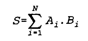
- the arrangement according to FIG. 1 is intended to be scalar products, that is to say expressions of the form be determined.
- the individual values A i and B i are stored since they are required at defined times.
- the subtotal formed after the last product is then also the end result.
- the time t 0 at the end of a second cycle time T2 thus represents an arbitrarily selected time within the processing of the chain of products.
- the one factor A i of the product P i currently to be formed which is off during this cycle time T2 the memory arrangement 12 has been read out, written into the register 16, specifically by the rising signal on the line 8 for the first clock time T1.
- the previous product P i-1 formed in the multiplier 20 is written into the product register 22.
- the partial sum registers 30 and 32 are not yet considered in detail here.
- the second value B i of the product to be formed is read out of the memory arrangement 12 and fed to the input of the register 18 via the data bus 14.
- the low signal on the control line 9 during this cycle time controls the multiplexer 24 in such a way that the connection 29 with the least significant bits of the product P i-1 is coupled to the input 25 of the adder arrangement 26, and at the same time it is connected in the same way controlled multiplexer 34, the output 33 of the partial sum register 32 is coupled to the input 35 of the adder arrangement 26.
- the half of the lowest valency of the partial sum formed in this way is written into the second sum register 32, and at the same time this is done via the Output 27a transmitted transmission signal written in the carry memory 28.
- the second factor B i of the product to be formed is written into the register 18.
- the two multiplexers 24 and 34 are switched so that the input 25 of the adder arrangement 26 now receives the bits of the highest value of the product P i-1 at the output 23 of the product register 22, the content of which has remained unchanged, and at the same time the input 35 receives the adder arrangement 26 contains the bits of higher significance of the previous partial sum contained in the first partial sum register 30 and also the carry from the carry memory 28 output at the output 37, so that the part of highest significance of the new subtotal is now formed in the adder arrangement 26 and output at the output 27, and at the same time the multiplier arrangement 20 forms the next product P i , since both values A i and B i are now present in the registers 16 and 18.
- the control arrangement 10 addresses the first value A i + 1 for the following product P i + 1 and feeds this value to the register 16, inter alia, via the bus 14.
Description
Die Erfindung betrifft ein Verfahren zum Bilden der Summe einer Kette von Produkten aus je zwei Zahlen, die nacheinander zugeführt werden, wobei jedes Zwischenergebnis der Summenbildung zwischengespeichert wird, sowie eine Anordnung zum Bilden der Summe einer Kette von Produkten aus jeweils einem ersten und einem zweiten Wert, mit einer Speicheranordnung zum Speichern einer Anzahl von Werten mit einer vorgegebenen ersten Anzahl Bits, einer taktgesteuerten Steueranordnung zum Steuern des Einschreibens von Werten in Register, einer ersten Registeranordnung zum Aufnehmen von jeweils zwei miteinander zu multiplizierenden Werten, einer Multiplizieranordnung mit zwei Eingängen, die mit der ersten Registeranordnung verbunden sind, und einem nachgeschalteten Produktregister mit einem Ausgang für die doppelte erste Anzahl Bits, einer Addieranordnung mit zwei Summeneingängen für je die erste Anzahl Bits, von denen der eine mit dem Ausgang des Produktregisters koppelbar ist, und einem nachgeschalteten Summenregister aus wenigstens zwei Teilsummenregistern für je die erste Anzahl Bits, mit einem Ausgang, der mit dem anderen Eingang der Addieranordnung koppelbar ist.The invention relates to a method for forming the sum a chain of products made up of two numbers one after the other are supplied, each intermediate result of the Sum formation is cached, as well as an arrangement to form the sum of a chain of products a first and a second value each, with a Storage arrangement for storing a number of values with a predetermined first number of bits, a clock-controlled Control arrangement for controlling the registered mail of values in registers, a first register arrangement for Record two each to be multiplied Values, a multiplication arrangement by two Inputs connected to the first register arrangement and a downstream product register with a Output for twice the first number of bits, an adding arrangement with two total inputs for the first number each Bits, one of which is connected to the output of the product register can be coupled, and a downstream sum register from at least two subtotals for each the first number of bits, with an output connected to the other input of the adder arrangement can be coupled.
Derartige Verfahren treten häufig auf bei der digitalen Signalverarbeitung, beispielsweise beim Filtern von Signalverläufen, und derartige Anordnungen werden bei vielen Vielzweck-Signalprozessoren verwendet Um Signalfolgen mit hoher Frequenz verarbeiten zu können, weisen übliche Signalprozessoren zwei Datenbusse auf, um in jeder Taktzeit ein neues Produkt bilden zu können. Da dieses Produkt außerdem die doppelte Anzahl Bits, d.h. die doppelte Wortbreite aufweist, ist die Addieranordnung auch für die doppelte Wortbreite ausgelegt. Dies stellt jedoch einen relativ hohen Aufwand dar.Such methods often occur in the digital Signal processing, for example when filtering Waveforms, and such arrangements are at many multipurpose signal processors used to signal sequences to be able to process at high frequency Usual signal processors have two data buses to go in each Cycle time to form a new product. Since this Product also double the number of bits, i.e. the has twice the word width, the adder is also designed for double the word width. However, this poses a relatively high effort.
Derartige Anordnungen sind in dem Artikel Electrical Design News, Band 26, Nummer 7, April 01, 1981, Seiten 153-163 veröfentlicht.Such arrangements are published in Electrical Design News,
Aufgabe der Erfindung ist es, ein Verfahren der eingangs genannten Art anzugeben, die die Bildung der Summe einer Kette von Produkten mit wenig Aufwand bei nur wenig verringerter Geschwindigkeit ermöglicht.The object of the invention is a method of the beginning Specify the type specified, which is the formation of the sum of a Chain of products with little effort with only a little reduced Allows speed.
Diese Aufgabe wird gemäß Anspruch 1 dadurch gelöst, daß
bei jeder einzelnen Multiplikation das entstehende Produkt zwischengespeichert wird und in
zwei Schritten zum Zwischenergebnis addiert wird, indem im
ersten Schritt nur die Stellen niedrigster Wertigkeit des
Produkts zu den entsprechenden Stellen des Zwischenergebnisses
addiert und die dabei entstehende erste Teilsumme
zwischengespeichert wird und im zweiten Schritt die
restlichen Stellen höherer Wertigkeit des Produkts zu den
entsprechenden restlichen Stellen der Zwischensumme und
dem Übertrag der ersten Teilsumme addiert und die dabei
entstehende zweite Teilsumme zwischengespeichert wird,
wobei in jedem Schritt eine andere der unmittelbar
anschließend zu multiplizierenden Zahlen zugeführt wird.This object is achieved according to
Eine weitere Aufgabe der Erfindung besteht darin, eine Anordnung der eingangs genannten Art anzugeben, die das Bilden der Summe einer Kette von Produkten mit weniger Aufwand bei nur wenig verringerter Geschwindigkeit ermöglicht.Another object of the invention is to provide a Specify an arrangement of the type mentioned that the Form the sum of a chain of products with less Effort with only a slightly reduced speed enables.
Diese Aufgabe wird gemäß Anspruch 2 dadurch gelöst, daß die
Speicheranordnung (12) über nur einen Datenbus (14) für
die erste Anzahl Bits mit der ersten Registeranordnung
(16,18) verbunden ist und daß die Steueranordnung (10)
eingerichtet ist, um abwechselnd in einer ersten und einer
zweiten Taktzeit zu arbeiten und in der ersten Taktzeit
die erste Anzahl Bits niedrigster Wertigkeit am Ausgang
des Produktregisters (22) und den Inhalt des zweiten Teilsummenregisters
(32) den Eingängen der Addieranordnung
(26) zuzuführen und am Ende dieser Taktzeit einen der
ersten Werte (Bi) in die Registeranordnung (16) und die am
Ausgang der Addieranordnung (26) vorhandene neue Teilsumme
in das zweite Teilsummenregister (32) einzuschreiben und
in der zweiten Taktzeit die erste Anzahl Bits höchster
Wertigkeit am Ausgang des Produktregisters (22) und den
Inhalt des ersten Teilsummenregisters sowie einen zwischengespeicherten
Übertrag der Addieranordnung (26) zuzuführen
und am Ende dieser Taktzeit einen der zweiten Werte
(Ai+1) in die Registeranordnung (16,18) und die am Ausgang
der Addieranordnung (26) vorhandene zweite Teilsumme in
das erste Teilsummenregister sowie das von der Multiplizieranordnung
(20) gebildete Produkt in das Produktregister
(22) einzuschreiben.This object is achieved according to
Jede vollständige Teilsumme wird dabei also in zwei Taktzeiten gebildet, so daß die Verarbeitungsgeschwindigkeit insgesamt halbiert ist. Dafür ist jedoch nur ein einfacher Datenbus erforderlich, über den die zu verarbeitenden Werte nacheinander übertragen werden, und es ist ferner auch eine Addieranordnung mit nur der einfachen Wortbreite ausreichend, die die Teilsummen in den beiden Taktzeiten nacheinander bestimmt. Da zunächst nur die Teilsumme aus den Bits niedrigster Wertigkeit gebildet wird, steht für die Bildung der zweiten Teilsumme der Übertrag aus der ersten Teilsumme jeweils zur Verfügung. Dadurch entstehen keine Rundungsfehler, da alle vorhandenen Stellen tatsächlich ausgewertet werden, während das genaue Ergebnis schließlich dem zweiten Teilsummenregister entnommen werden kann.Each complete partial sum is thus in two cycle times formed so that the processing speed is halved overall. However, this is just a simple one Data bus required over which to be processed Values are transferred sequentially and it is further also an adder arrangement with only the simple word width sufficient that the subtotals in the two cycle times determined one after the other. Since initially only the partial sum The bits with the lowest value are formed for the formation of the second subtotal of the carry over from the first subtotal available. This creates no rounding errors, since all existing positions are actually be evaluated while the exact result finally taken from the second partial total register can be.
Ein Ausführungsbeispiel der Erfindung wird nachstehend
anhand der Zeichnung näher erläutert. Es zeigen
In Fig. 1 erzeugt eine Steueranordnung 10 zwei Steuersignale
T1 und T2 auf den Leitungen 8 und 9, die sich
zyklisch abwechseln. Ferner erzeugt die Steueranordnung 10
an einem Ausgang 11 Adressen zur Adressierung einer
Speicheranordnung 12. Die Verbindung 11 ist hier doppelt
gezeichnet, da diese tatsächlich aus einer Anzahl
paralleler Leitungen besteht, über die die Bits einer
Adresse parallel übertragen werden. Dies gilt auch für die
ebenfalls doppelt gezeichneten Datenverbindungen, die
ebenfalls tatsächlich aus mehreren Leitungen bestehen,
über die die Bits jeweils eines Datenworts parallel übertragen
werden.1, a
Der Datenanschluß der Speicheranordnung 12, die auch aus
mehreren einzelnen Speichern einschließlich gegebenenfalls
Festwertspeichern bestehen kann, ist mit einem Datenbus 14
verbunden, an den außer weiteren, nicht dargestellten
Einrichtungen eines Prozessors die beiden Register 16 und
18 parallel angeschlossen sind. Das Einschreiben in diese
Register wird durch Steuersignale auf den Leitungen 8 und
9 gesteuert.The data connector of the
Die Ausgänge 17 und 19 der Register 16 und 18, die zum
Aufnehmen der miteinander zu multiplizierenden Faktoren
bestimmt sind, sind mit den Eingängen einer Multiplizieranordnung
20 verbunden, die innerhalb einer Taktzeit das
vollständige Produkt der beiden über die Verbindungen 17
und 19 zugeführten Werte bildet und das Produkt am Ausgang
21 abgibt. Dieses weist die doppelte Wortbreite, d.h.
die doppelte Anzahl Bits der zugeführten Faktoren auf.
Dies ist die einzige Stelle innerhalb der Anordnung nach
Fig. 1, an der eine doppelte Wortbreite auftritt, und die
Verbindung 21 ist mit dem Eingang eines Produktregisters
22 verbunden, das ebenfalls für diese doppelte
Wortbreite ausgelegt ist.The
An das Produktregister 22 sind ausgangsseitig zwei Verbindungen
23 und 29 angeschlossen, von denen die Verbindung
23 die Bits höchster Wertigkeit und die Verbindung
29 die Bits niedrigster Wertigkeit führt, d.h. jede
Verbindung hat die einfache Wortbreite. Die Verbindungen
23 und 29 führen auf einen Multiplexer, der über
ein Steuersignal auf der Leitung 8 gesteuert die Verbindung
23 oder die Verbindung 29 mit einem Eingang 25 einer
Addieranordnung 26 verbindet. Der andere Eingang 35 der
Addieranordnung 26 ist mit dem Ausgang eines zweiten
Multiplexers 34 verbunden.On the output side there are two connections to the
Der Summenausgang 27 des Addierers 26 führt parallel auf
die Eingänge zweier Teilsummenregister 30 und 32, die über
die Steuerleitungen 8 und 9 abwechselnd zum Einschreiben
angesteuert werden. Bei dem zweiten Teilsummenregister 32
ist ferner ein Ubertragspeicher 28 vorgesehen, in den
parallel zum zweiten Summenregister der am Ausgang 27a der
Addieranordnung 26 auftretende Übertrag über die Steuerleitung
8 eingeschrieben wird.The
Die Ausgänge 31 und 33 der Teilsummenregister 30 und 32
führen auf die beiden Eingänge des Multiplexers 34, der
über die Steuerleitung 8 gesteuert entweder den Ausgang 31
zusammen mit dem Ausgang 37 des Übertragspeichers 28 oder
den Ausgang 33 mit dem zweiten Eingang 35 der Addieranordnung
26 verbindet. Der Ausgang 31 führt ferner am Ende der
Verarbeitung der Kette von Produkten die gesuchte Summe. The
Es ist jedoch häufig zweckmäßig, wenn auch der Inhalt des
Registers 32 ausgelesen und anderen Elementen zugeführt
werden kann.However, it is often useful if the content of the
Die Funktion der Anordnung nach Fig. 1 wird nun anhand des
schematischen Zeitdiagramms in Fig. 2 erläutert, in der
die Zahlen vor den einzelnen Zeilen die Signale bzw. Werte
auf den Verbindungen bzw. die Inhalte der Blöcke mit den
betreffenden Bezugszeichen angeben. Mit der Anordnung nach
Fig. 1 sollen Skalarprodukte, also Ausdrücke der Form
Bei dem Zeitdiagramm in Fig. 2 wird zunächst davon ausgegangen,
daß die ersten Produkte bereits verarbeitet sind
und die entsprechende Zwischensumme gebildet ist. Der
Zeitpunkt t0 am Ende einer zweiten Taktzeit T2 stellt also
einen willkürlich gewählten Zeitpunkt innerhalb der Verarbeitung
der Kette von Produkten dar. Zu diesem Zeitpunkt
t0 wird der eine Faktor Ai des aktuell zu bildenden
Produkts Pi, der während dieser Taktzeit T2 aus der
Speicheranordnung 12 ausgelesen wurde, in das Register 16
eingeschrieben, und zwar durch das ansteigende Signal auf
der Leitung 8 für die erste Taktzeit T1. Gleichzeitig wird
das in der Multiplizieranordnung 20 gebildete vorhergehende
Produkt Pi-1 in das Produktregister 22 eingeschrieben.
Die Teilsummenregister 30 und 32 werden an
dieser Stelle noch nicht näher betrachtet.In the time diagram in FIG. 2, it is initially assumed that the first products have already been processed and that the corresponding subtotal has been formed. The time t 0 at the end of a second cycle time T2 thus represents an arbitrarily selected time within the processing of the chain of products. At this time t 0 , the one factor A i of the product P i currently to be formed, which is off during this cycle time T2 the
In der folgenden Taktzeit T1 nach dem Zeitpunkt t0 wird der
zweite Wert Bi des zu bildenden Produktes aus der Speicheranordnung
12 ausgelesen und über den Datenbus 14 dem Eingang
des Registers 18 zugeführt. Durch das niedrige Signal
auf der Steuerleitung 9 während dieser Taktzeit wird der
Multiplexer 24 so gesteuert, daß die Verbindung 29 mit den
Bits niedrigster Wertigkeit des Produktes Pi-1 dem Eingang
25 der Addieranordnung 26 gekoppelt ist, und
gleichzeitig wird über den in gleicher Weise gesteuerten
Multiplexer 34 der Ausgang 33 des Teilsummenregisters 32
mit dem Eingang 35 der Addieranordnung 26 gekoppelt. Diese
bildet während der Taktzeit T1 die Teilsumme SL i-1 und gibt
diese gegen Ende der Taktzeit T1 am Ausgang 27 ab.In the following cycle time T1 after the time t 0 , the second value B i of the product to be formed is read out of the
Am Ende der Taktzeit T1, nämlich zum Zeitpunkt t1, wenn das
Signal auf der Steuerleitung 8 niedrig und auf der Steuerleitung
9 hoch wird, wird die so gebildete Hälfte
niedrigster Wertigkeit der Teilsumme in das zweite Summenregister
32 eingeschrieben, und gleichzeitig wird das über
den Ausgang 27a abgegebene Ubertragsignal in den Übertragspeicher
28 eingeschrieben. Außerdem wird der zweite
Faktor Bi des zu bildenden Produktes in das Register 18
eingeschrieben. Ferner werden die beiden Multiplexer 24
und 34 umgeschaltet, so daß nun der Eingang 25 der Addieranordnung
26 die Bits höchster Wertigkeit des Produktes Pi-1
am Ausgang 23 des Produktregisters 22, dessen Inhalt
unverändert geblieben ist, empfängt, und gleichzeitig
empfängt der Eingang 35 der Addieranordnung 26 die im
ersten Teilsummenregister 30 enthaltenen Bits höherer
Wertigkeit der vorhergehenden Teilsumme sowie außerdem den
am Ausgang 37 abgegebenen Übertrag aus dem Übertragspeicher
28, so daß nun der Teil höchster Wertigkeit der
neuen Zwischensumme in der Addieranordnung 26 gebildet und
am Ausgang 27 abgegeben wird, und gleichzeitig bildet die
Multiplizieranordnung 20 das nächste Produkt Pi, da nun
beide Werte Ai und Bi in den Registern 16 und 18 vorliegen.
Außerdem adressiert die Steueranordnung 10 den ersten
Wert Ai+1 für das folgende Produkt Pi+1 und führt diesen Wert
über den Bus 14 u.a. dem Register 16 zu.At the end of the cycle time T1, namely at time t 1 , when the signal on the
Am Ende der Taktzeit T2, zum Zeitpunkt t2, wird nun das
Steuersignal auf der Leitung 8 hoch, so daß der Wert Ai+1 in
das Register 16 eingeschrieben wird, und gleichzeitig wird
das vom Multiplizierer 20 am Ausgang 21 abgegebene Produkt
Pi in das Produktregister 22 eingeschrieben, und ferner
wird der Teil höchster Wertigkeit der vorhergehenden
Zwischensumme SH i-1 in das erste Teilsummenregister 30
eingeschrieben. Damit ist die Verarbeitung des Produktes
Pi-1 abgeschlossen, und das nun im Produktregister 22
enthaltene Produkt Pi kann weiterverarbeitet werden.At the end of the cycle time T2, at the time t 2 , the control signal on the
Dies geschieht in der zweiten dargestellten Taktphase T1,
in der der Multiplexer 24 wieder umgeschaltet wird und die
Bits niedrigster Wertigkeit des Produktes Pi am Ausgang 29
des Produktregisters 22 dem Eingang 25 der Addieranordnung
26 zuführt. Gleichzeitig erhält der andere Eingang 35
der Addieranordnung 26 die vorhergehende Teilsumme SL i-1
über den Multiplexer 34 vom Ausgang 33 des zweiten Teilsummenregisters
32, und die neue Teilsumme niedrigster
Wertigkeit SL i wird am Ausgang 27 der Addieranordnung 26
erzeugt und am Ende der Taktzeit T1, zum Zeitpunkt t3, in
das zweite Teilsummenregister 32 eingeschrieben. Gleichzeitig
wird im übrigen der zweite Wert Bi+1, der während der
Taktzeit T1 ausgelesen wurde, in das Register 18 eingeschrieben.This takes place in the second clock phase T1 shown, in which the
In der dritten dargestellten Taktzeit T2 wird nun am
Ausgang 21 des Multiplizierers 20 das folgende gültige
Produkt Pi+1 gebildet, und gleichzeitig werden dem Eingang
25 der Addieranordnung 26 die Bits höchster Wertigkeit
aus dem Produktregister 22 und dem Eingang 35 die
vorhergehende Teilsumme höchster Wertigkeit SH i-1 des ersten
Teilsummenregisters 30 sowie das Übertragsignal vom Übertragspeicher
28 zugeführt, so daß die neue Teilsumme
höchster Wertigkeit SH i am Ausgang 27 der Addieranordnung
26 gebildet wird. Diese wird am Ende der dritten
dargestellten Taktzeit T2 wieder in das erste Teilsummenregister
30 eingeschrieben.In the third cycle time T2 shown, the following valid product P i + 1 is now formed at the
Dieser Vorgang setzt sich zyklisch fort, bis alle Produkte der Kette berechnet und durch Aufakkumulieren in die Teilsummenregister verarbeitet sind. Wie aus Fig. 2 zu erkennen ist, erfolgt die Verarbeitung dabei nach dem Fließbandprinzip, d.h. während ein Produkt gebildet wird, wird gleichzeitig die vorhergehende Teilsumme gebildet und die Werte des nachfolgenden Produktes zugeführt. Am Anfang, d.h. bei der Bildung des ersten Produktes P1, sind daher einige Verarbeitungsschritte vorab erforderlich.This process continues cyclically until all products in the chain are calculated and processed by accumulation in the partial total register. As can be seen from FIG. 2, the processing is carried out according to the assembly line principle, ie while a product is being formed, the previous partial sum is simultaneously formed and the values of the subsequent product are added. At the beginning, ie when the first product P 1 is formed , some processing steps are therefore necessary in advance.
Diese sind aus Fig. 2 ersichtlich, wenn i = 1 gesetzt
wird. Das bedeutet, daß vor dem Zeitpunkt t0 zunächst der
eine Wert A1 ausgelesen und zum Zeitpunkt t0 in das
Register eingeschrieben werden muß. Danach wird der zweite
Wert B1 ausgelesen und zum Zeitpunkt t1 in das Register 18
eingeschrieben. Danach kann das erste Produkt P1 gebildet
werden, das zum Zeitpunkt t2 in das Produktregister 22
eingeschrieben wird. Nun kann das Produkt P1 in der bereits
beschriebenen Weise verarbeitet werden, wobei während
dieser vorhergehenden Verarbeitungsschritte die Teilsummenregister
30 und 32 selbstverständlich gelöscht sein
müssen, d.h. sie müssen den Wert Null enthalten. These can be seen from FIG. 2 if i = 1 is set. This means that before time t 0 , a value A 1 must first be read out and written into the register at time t 0 . The second value B 1 is then read out and written into the
Auf diese Weise wird die Summe einer Kette von Produkten gebildet, wobei die volle Genauigkeit ohne Rundungsfehler erhalten bleibt und dennoch nur ein Addierer für die einfache Wortbreite erforderlich ist.This way the sum of a chain of products formed, the full accuracy without rounding errors is preserved and yet only an adder for the simple Word width is required.
Claims (3)
- A method of forming the sum of a chain of products of each time two numbers which are successively supplied, each intermediate result of the summing operation being temporarily stored, characterized in that the product produced by each separate multiplication is temporarily stored and added to the intermediate result in two steps, in that during the first step only the least-significant positions of the product are added to the corresponding positions of the intermediate result, the first partial sum thus formed being temporarily stored, whereas during the second step the remaining, more-significant positions of the product are added to the corresponding remaining positions of the intermediate sum and the carry of the first partial sum, the second partial sum thus formed being temporarily stored, during each step there being supplied another one of the numbers to be directly subsequently multiplied.
- A device for forming the sum of a chain of products of each time a first and a second value, comprising a storage device for storing a number of values with a predetermined first number of bits, a clock-controlled control device for controlling the writing of values in registers, a first register device for storing each time two values to be multiplied by one another, a multiplier device comprising two inputs which are connected to the first register device, and a downstream product register which comprises an output for double the first number of bits, an adder device which comprises two sum inputs for each time the first number of bits, one of said inputs being connectable to the output of the product register, and a downstream sum register which consists of at least two partial sum registers for each time the first number of bits, comprising an output which can be coupled to the other input of the adder device, characterized in that the storage device (12) is connected to the first register device (16, 18) via only one data bus (14) for the first number of bits, and that the control device (10) is arranged to operate alternately in a first and a second clock period and to apply, during the first clock period, the first number of least-significant bits at the output of the product register (22) and the contents of the second partial sum register (32) to the inputs of the adder device (26), and to write, at the end of this clock period, one of the first values (Bi) into the register device (16) and the new partial sum, appearing at the output of the adder device (26), into the second partial sum register (32), and to apply, during the second clock period, the first number of most-significant bits at the output of the product register (22) and the content of the first partial sum register as well as a temporarily stored carry to the adder device (26) and to write, at the end of this clock period, one of the second values (Ai+1) into the register device (16, 18) and the second partial sum, appearing at the output of the adder device (26), into the first partial sum register as well as to write the product formed by the multiplier device (20) into the product register (22).
- A device as claimed in Claim 2, characterized in that between the output of the product register (22) and one sum input of the adder device (26) there is connected a first multiplexer (24), whereas a second multiplexer (34) is connected between the outputs of the partial sum registers (30, 32) and the other input of the adder device (26), and that the control device (10) is arranged to switch over the multiplexers after each clock period.
Applications Claiming Priority (3)
| Application Number | Priority Date | Filing Date | Title |
|---|---|---|---|
| DE4218769 | 1992-06-06 | ||
| DE4218769A DE4218769A1 (en) | 1992-06-06 | 1992-06-06 | Method and arrangement for forming the sum of a chain of products |
| PCT/NL1993/000117 WO1993025959A1 (en) | 1992-06-06 | 1993-06-04 | Process and configuration for establishing the sum of a chain of products |
Publications (2)
| Publication Number | Publication Date |
|---|---|
| EP0598112A1 EP0598112A1 (en) | 1994-05-25 |
| EP0598112B1 true EP0598112B1 (en) | 1999-06-16 |
Family
ID=6460574
Family Applications (1)
| Application Number | Title | Priority Date | Filing Date |
|---|---|---|---|
| EP93916269A Expired - Lifetime EP0598112B1 (en) | 1992-06-06 | 1993-06-04 | Process and configuration for establishing the sum of a chain of products |
Country Status (6)
| Country | Link |
|---|---|
| US (1) | US5602766A (en) |
| EP (1) | EP0598112B1 (en) |
| JP (1) | JPH07501167A (en) |
| KR (1) | KR100271074B1 (en) |
| DE (2) | DE4218769A1 (en) |
| WO (1) | WO1993025959A1 (en) |
Families Citing this family (8)
| Publication number | Priority date | Publication date | Assignee | Title |
|---|---|---|---|---|
| FR2718866B1 (en) * | 1994-04-19 | 1996-05-15 | Sgs Thomson Microelectronics | Arithmetic and logic calculation device and control method. |
| WO1996032676A1 (en) * | 1995-04-12 | 1996-10-17 | Strakhov, Sergei Vitalievich | Method and device for computing product sums |
| US5784306A (en) * | 1996-06-28 | 1998-07-21 | Cirrus Logic, Inc. | Parallel multiply accumulate array circuit |
| DE19637369C2 (en) * | 1996-09-13 | 2001-11-15 | Micronas Gmbh | Digital signal processor with multiplier and method |
| US5847981A (en) * | 1997-09-04 | 1998-12-08 | Motorola, Inc. | Multiply and accumulate circuit |
| FR2775368B1 (en) * | 1998-02-26 | 2000-04-14 | Sgs Thomson Microelectronics | MODULAR ARITHMETIC CO-PACKER FOR QUICKLY UNMODULATED OPERATIONS |
| US6484194B1 (en) * | 1998-06-17 | 2002-11-19 | Texas Instruments Incorporated | Low cost multiplier block with chain capability |
| US7266580B2 (en) * | 2003-05-12 | 2007-09-04 | International Business Machines Corporation | Modular binary multiplier for signed and unsigned operands of variable widths |
Family Cites Families (4)
| Publication number | Priority date | Publication date | Assignee | Title |
|---|---|---|---|---|
| DE3577242D1 (en) * | 1984-08-14 | 1990-05-23 | Trt Telecom Radio Electr | PROCESSOR FOR PROCESSING DATA OF DIFFERENT PRESENTATION PRESENTATIONS AND SUITABLE MULTIPLIER FOR SUCH A PROCESSOR. |
| US4809212A (en) * | 1985-06-19 | 1989-02-28 | Advanced Micro Devices, Inc. | High throughput extended-precision multiplier |
| US4754421A (en) * | 1985-09-06 | 1988-06-28 | Texas Instruments Incorporated | Multiple precision multiplication device |
| JPH07113886B2 (en) * | 1987-05-11 | 1995-12-06 | 株式会社日立製作所 | Arithmetic circuit |
-
1992
- 1992-06-06 DE DE4218769A patent/DE4218769A1/en not_active Withdrawn
-
1993
- 1993-06-04 EP EP93916269A patent/EP0598112B1/en not_active Expired - Lifetime
- 1993-06-04 DE DE59309652T patent/DE59309652D1/en not_active Expired - Fee Related
- 1993-06-04 WO PCT/NL1993/000117 patent/WO1993025959A1/en active IP Right Grant
- 1993-06-04 US US08/190,068 patent/US5602766A/en not_active Expired - Fee Related
- 1993-06-04 JP JP6501341A patent/JPH07501167A/en active Pending
- 1993-06-04 KR KR1019940700362A patent/KR100271074B1/en not_active IP Right Cessation
Also Published As
| Publication number | Publication date |
|---|---|
| KR100271074B1 (en) | 2000-11-01 |
| EP0598112A1 (en) | 1994-05-25 |
| DE4218769A1 (en) | 1993-12-09 |
| DE59309652D1 (en) | 1999-07-22 |
| US5602766A (en) | 1997-02-11 |
| JPH07501167A (en) | 1995-02-02 |
| WO1993025959A1 (en) | 1993-12-23 |
Similar Documents
| Publication | Publication Date | Title |
|---|---|---|
| DE1549476C3 (en) | Order to execute divisions | |
| EP0115609B1 (en) | Addressing device for the storage of several data processing units in a bus system | |
| DE2311220A1 (en) | DIGITAL INFORMATION PROCESSING DEVICE FOR CHARACTER RECOGNITION | |
| DE2619418A1 (en) | METHOD AND DEVICE FOR CONVERTING A BINARY NUMBER INTO A NUMBER MODULO M | |
| DE3632639C2 (en) | Device for high-speed processing of image data by folding | |
| DE2934344C2 (en) | ||
| DE2854782C2 (en) | Data processing system and method for replacing a block of data in high-speed storage | |
| EP0598112B1 (en) | Process and configuration for establishing the sum of a chain of products | |
| DE3507584C2 (en) | ||
| EP0265555B1 (en) | Method and circuitry for addition of floating point numbers | |
| DE4010735C2 (en) | ||
| DE2451235A1 (en) | CIRCUIT ARRANGEMENT FOR A DIGITAL FILTER | |
| DE2039228A1 (en) | Method and device for converting and shifting the value of number signals of different codes in a data processing system | |
| DE3535215C2 (en) | ||
| DE3416536C2 (en) | ||
| DE19637369C2 (en) | Digital signal processor with multiplier and method | |
| DE2840471A1 (en) | Calculator for digital filter - has central unit which outputs prod. sum of weighted signal values fed from external store by control unit | |
| DE2601379C3 (en) | Circuit arrangement for converting virtual addresses into real addresses | |
| DE1181459B (en) | Multiplication circuit for electronic number calculators | |
| DE1234055B (en) | Arrangement for addition or subtraction | |
| DE2150292C2 (en) | Microprogram-controlled data processing system with superimposed execution and extraction of commands | |
| DE1958662A1 (en) | Digital pulse train divider with optimal uniform distribution of the pulses of an output pulse train selected from an equidistant input pulse train | |
| EP0161335B1 (en) | Preparation of sampled values of a time-variable signal in a data processing arrangement | |
| DE2142636B2 (en) | Simplified digital multiplier for computers - uses parallel fed multiplicand(s) and partial multipliers with hard wired adders | |
| DE60024116T2 (en) | METHOD FOR AUTOMATIC ARRANGEMENT OF THE TASKS OF AN APPLICATION IN A SIGNAL PROCESSING MACHINE |
Legal Events
| Date | Code | Title | Description |
|---|---|---|---|
| PUAI | Public reference made under article 153(3) epc to a published international application that has entered the european phase |
Free format text: ORIGINAL CODE: 0009012 |
|
| AK | Designated contracting states |
Kind code of ref document: A1 Designated state(s): CH DE ES FR GB IT LI NL SE |
|
| 17P | Request for examination filed |
Effective date: 19940125 |
|
| GRAG | Despatch of communication of intention to grant |
Free format text: ORIGINAL CODE: EPIDOS AGRA |
|
| 17Q | First examination report despatched |
Effective date: 19980702 |
|
| GRAG | Despatch of communication of intention to grant |
Free format text: ORIGINAL CODE: EPIDOS AGRA |
|
| GRAG | Despatch of communication of intention to grant |
Free format text: ORIGINAL CODE: EPIDOS AGRA |
|
| GRAH | Despatch of communication of intention to grant a patent |
Free format text: ORIGINAL CODE: EPIDOS IGRA |
|
| GRAH | Despatch of communication of intention to grant a patent |
Free format text: ORIGINAL CODE: EPIDOS IGRA |
|
| GRAA | (expected) grant |
Free format text: ORIGINAL CODE: 0009210 |
|
| AK | Designated contracting states |
Kind code of ref document: B1 Designated state(s): CH DE ES FR GB IT LI NL SE |
|
| PG25 | Lapsed in a contracting state [announced via postgrant information from national office to epo] |
Ref country code: SE Free format text: THE PATENT HAS BEEN ANNULLED BY A DECISION OF A NATIONAL AUTHORITY Effective date: 19990616 Ref country code: NL Free format text: LAPSE BECAUSE OF FAILURE TO SUBMIT A TRANSLATION OF THE DESCRIPTION OR TO PAY THE FEE WITHIN THE PRESCRIBED TIME-LIMIT Effective date: 19990616 Ref country code: IT Free format text: LAPSE BECAUSE OF FAILURE TO SUBMIT A TRANSLATION OF THE DESCRIPTION OR TO PAY THE FEE WITHIN THE PRE;WARNING: LAPSES OF ITALIAN PATENTS WITH EFFECTIVE DATE BEFORE 2007 MAY HAVE OCCURRED AT ANY TIME BEFORE 2007. THE CORRECT EFFECTIVE DATE MAY BE DIFFERENT FROM THE ONE RECORDED.SCRIBED TIME-LIMIT Effective date: 19990616 Ref country code: ES Free format text: THE PATENT HAS BEEN ANNULLED BY A DECISION OF A NATIONAL AUTHORITY Effective date: 19990616 |
|
| REG | Reference to a national code |
Ref country code: CH Ref legal event code: EP |
|
| REF | Corresponds to: |
Ref document number: 59309652 Country of ref document: DE Date of ref document: 19990722 |
|
| REG | Reference to a national code |
Ref country code: CH Ref legal event code: PK |
|
| RAP2 | Party data changed (patent owner data changed or rights of a patent transferred) |
Owner name: KONINKLIJKE PHILIPS ELECTRONICS N.V. Owner name: PHILIPS PATENTVERWALTUNG GMBH |
|
| GBT | Gb: translation of ep patent filed (gb section 77(6)(a)/1977) |
Effective date: 19990722 |
|
| ET | Fr: translation filed | ||
| NLV1 | Nl: lapsed or annulled due to failure to fulfill the requirements of art. 29p and 29m of the patents act | ||
| RAP4 | Party data changed (patent owner data changed or rights of a patent transferred) |
Owner name: KONINKLIJKE PHILIPS ELECTRONICS N.V. Owner name: PHILIPS CORPORATE INTELLECTUAL PROPERTY GMBH |
|
| PLBE | No opposition filed within time limit |
Free format text: ORIGINAL CODE: 0009261 |
|
| STAA | Information on the status of an ep patent application or granted ep patent |
Free format text: STATUS: NO OPPOSITION FILED WITHIN TIME LIMIT |
|
| 26N | No opposition filed | ||
| PG25 | Lapsed in a contracting state [announced via postgrant information from national office to epo] |
Ref country code: LI Free format text: LAPSE BECAUSE OF NON-PAYMENT OF DUE FEES Effective date: 20000630 Ref country code: CH Free format text: LAPSE BECAUSE OF NON-PAYMENT OF DUE FEES Effective date: 20000630 |
|
| REG | Reference to a national code |
Ref country code: CH Ref legal event code: PL |
|
| PGFP | Annual fee paid to national office [announced via postgrant information from national office to epo] |
Ref country code: FR Payment date: 20010625 Year of fee payment: 9 |
|
| PGFP | Annual fee paid to national office [announced via postgrant information from national office to epo] |
Ref country code: GB Payment date: 20010629 Year of fee payment: 9 |
|
| PGFP | Annual fee paid to national office [announced via postgrant information from national office to epo] |
Ref country code: DE Payment date: 20010821 Year of fee payment: 9 |
|
| REG | Reference to a national code |
Ref country code: GB Ref legal event code: IF02 |
|
| PG25 | Lapsed in a contracting state [announced via postgrant information from national office to epo] |
Ref country code: GB Free format text: LAPSE BECAUSE OF NON-PAYMENT OF DUE FEES Effective date: 20020604 |
|
| PG25 | Lapsed in a contracting state [announced via postgrant information from national office to epo] |
Ref country code: DE Free format text: LAPSE BECAUSE OF NON-PAYMENT OF DUE FEES Effective date: 20030101 |
|
| GBPC | Gb: european patent ceased through non-payment of renewal fee |
Effective date: 20020604 |
|
| PG25 | Lapsed in a contracting state [announced via postgrant information from national office to epo] |
Ref country code: FR Free format text: LAPSE BECAUSE OF NON-PAYMENT OF DUE FEES Effective date: 20030228 |
|
| REG | Reference to a national code |
Ref country code: FR Ref legal event code: ST |