EP0597653A2 - Radio frequency circuit for a time division multiple access system - Google Patents
Radio frequency circuit for a time division multiple access system Download PDFInfo
- Publication number
- EP0597653A2 EP0597653A2 EP93308904A EP93308904A EP0597653A2 EP 0597653 A2 EP0597653 A2 EP 0597653A2 EP 93308904 A EP93308904 A EP 93308904A EP 93308904 A EP93308904 A EP 93308904A EP 0597653 A2 EP0597653 A2 EP 0597653A2
- Authority
- EP
- European Patent Office
- Prior art keywords
- radio frequency
- transmit
- receive
- frequency circuit
- filter
- Prior art date
- Legal status (The legal status is an assumption and is not a legal conclusion. Google has not performed a legal analysis and makes no representation as to the accuracy of the status listed.)
- Granted
Links
Images
Classifications
-
- H—ELECTRICITY
- H04—ELECTRIC COMMUNICATION TECHNIQUE
- H04B—TRANSMISSION
- H04B1/00—Details of transmission systems, not covered by a single one of groups H04B3/00 - H04B13/00; Details of transmission systems not characterised by the medium used for transmission
- H04B1/38—Transceivers, i.e. devices in which transmitter and receiver form a structural unit and in which at least one part is used for functions of transmitting and receiving
- H04B1/40—Circuits
- H04B1/44—Transmit/receive switching
-
- H—ELECTRICITY
- H04—ELECTRIC COMMUNICATION TECHNIQUE
- H04B—TRANSMISSION
- H04B1/00—Details of transmission systems, not covered by a single one of groups H04B3/00 - H04B13/00; Details of transmission systems not characterised by the medium used for transmission
- H04B1/38—Transceivers, i.e. devices in which transmitter and receiver form a structural unit and in which at least one part is used for functions of transmitting and receiving
- H04B1/40—Circuits
- H04B1/403—Circuits using the same oscillator for generating both the transmitter frequency and the receiver local oscillator frequency
-
- H—ELECTRICITY
- H04—ELECTRIC COMMUNICATION TECHNIQUE
- H04B—TRANSMISSION
- H04B1/00—Details of transmission systems, not covered by a single one of groups H04B3/00 - H04B13/00; Details of transmission systems not characterised by the medium used for transmission
- H04B1/38—Transceivers, i.e. devices in which transmitter and receiver form a structural unit and in which at least one part is used for functions of transmitting and receiving
- H04B1/40—Circuits
- H04B1/50—Circuits using different frequencies for the two directions of communication
- H04B1/52—Hybrid arrangements, i.e. arrangements for transition from single-path two-direction transmission to single-direction transmission on each of two paths or vice versa
- H04B1/525—Hybrid arrangements, i.e. arrangements for transition from single-path two-direction transmission to single-direction transmission on each of two paths or vice versa with means for reducing leakage of transmitter signal into the receiver
-
- H—ELECTRICITY
- H04—ELECTRIC COMMUNICATION TECHNIQUE
- H04B—TRANSMISSION
- H04B1/00—Details of transmission systems, not covered by a single one of groups H04B3/00 - H04B13/00; Details of transmission systems not characterised by the medium used for transmission
- H04B1/38—Transceivers, i.e. devices in which transmitter and receiver form a structural unit and in which at least one part is used for functions of transmitting and receiving
- H04B1/40—Circuits
- H04B1/50—Circuits using different frequencies for the two directions of communication
- H04B1/52—Hybrid arrangements, i.e. arrangements for transition from single-path two-direction transmission to single-direction transmission on each of two paths or vice versa
Definitions
- the invention relates to a radio frequency circuit for a time division multiple access (TDMA) system.
- TDMA systems are used in digital mobile telephone systems, examples of which are the Personal Communication Network (PCN) and the Groupe Speciale Mobile (GSM) systems.
- PCN Personal Communication Network
- GSM Groupe Speciale Mobile
- the present invention seeks to provide economies in the cost and size of the transmitter/receiver units for such systems which has particular advantage in hand-held units.
- the transmitter/receiver units employ direct digital synthesis to achieve a modulated signal for transmission and digital demodulation techniques are also used.
- digital to analogue and analogue to digital convertors DACs and ADCs
- DACs and ADCs digital to analogue and analogue to digital convertors
- Limitations imposed by the DACs and ADCs require a low intermediate frequency as the input/output of the RF circuits. In turn this requires at least a two-stage heterodyning process with corresponding intermediate frequencies (IFs) and therefore at least two IF filters in each of the transmit and receive channels.
- Such filters are relatively bulky and costly and the present invention seeks to alleviate the problem.
- a radio frequency circuit for a transmitter/receiver in a time division multiple access system, the circuit having a transmit channel, a receive channel, at least one intermediate frequency filter and means responsive to whether the circuit is transmitting or receiving to switch the or at least one of the filters to the transmit or receive channel, thereby allowing the filter or filters to be shared by the transmit and receive channels.
- each switchable filter is bidirectional, having the capacity to filter signals passing through it in either direction.
- each switchable filter is a SAW filter.
- the switchable filters are physically connected to both the transmit and receive circuits and switching is effected by control voltages applied to components in the transmit and receive circuits to switch the circuits on and off alternatively.
- the first in the direction of the receive channel
- the second intermediate frequency may be in the range 80 to 160 MHz and more particularly in the range 120 to 140 MHz.
- this takes the form of a transconductance-C active filter in the receive channel for filtering the signal resulting from heterodyning the second intermediate frequency.
- the first IF filter (in the direction of the receive channel) is shared, as is preferred, then steps must be taken to ensure that the first IF is the same for transmit and receive.
- the transmit and receive frequencies are the same.
- a feature of the invention is to provide a first receiving stage/final transmitting stage which has a local oscillator automatically switchable on transmit/receive to change frequency so that the first receive intermediate frequency and final transmit intermediate frequency are the same.
- the unit has an antenna 1 which is interfaced to receive and transmit channels via a duplexer 2.
- the receive channel of the RF circuit operates in this example as follows.
- the duplexer 2 feeds an amplifier 3 which applies signals via a band-pass filter 4 to a mixer 5.
- a local oscillator provides a frequency of 1324 MHz to give sidebands of 389 and 2259 MHz.
- a first IF filter 6 is switched at this time to be in the receive channel and is set to pass the 389 MHz sideband as the first intermediate frequency.
- the receive channel includes a further amplifier 7, a mixer 8 and two further amplifier stages 9, 10.
- a second local oscillator LO2 supplies a frequency of 260 MHz to give sidebands of 129 and 649 MHz.
- a second IF filter 11 is switched at this time to the receive channel and is set to pass the 129 MHz sideband as the second IF.
- a further amplifier 12 supplies a mixer 13 which is also provided by a third local oscillator LO3 with a frequency of 130 MHz. This produces sidebands of 1 and 259 MHz.
- a transconductance-C active filter 14 rejects the 259 MHz sideband, leaving the 1MHz signal to be fed to the low frequency digital demodulator (not shown) via an analogue to digital convertor 15.
- the circuit In the transmit mode the circuit automatically switches over the channels and places the IF filters 6 and 11 in the transmit channel.
- Appropriate switches are shown symbolically at 16, 17, 18 and 19 but it is to be understood that switching is effected by biasing amplifiers in the channels which are physically permanently connected to the IF filters.
- 1 MHz signals from the low frequency digital modulator (not shown) are applied to the transmit channel via a digital to analogue convertor 20 and a low stop filter 21 to an amplifier 22, a mixer 23 and a further amplifier 24.
- mixer 23 sidebands of 129 and 131 MHz are produced with the signal from local oscillator LO3.
- the 129 MHz signal is selected by filter 11.
- This and filter 6 are bidirectional SAW filters, operating similarly on signals passing in either direction.
- the 129MHz IF is mixed with the LO2 signal in mixer after passing through an amplifier 26. This produces sidebands of 389 and 131 MHz of which the 389 MHz signal is selected by filter 6 as the IF. This passes to a mixer 26. Instead of the receive frequency of 1324 MHz the local oscillator LO1 is now switched to produce a transmit frequency of 1729 MHz. This produces sidebands of 890 and 2188 MHz. The 2118 MHz signal is rejected by a filter 27 to allow the broadcast frequency of 890 MHz to be transmitted.
- a bandwidth of 300 KHz is required.
- the transmit requirements were to reject image frequencies and local oscillator leakage while passing the modulated transmit signal.
- the filter had to have a very carefully specified phase distortion in order that the global phase specification could be met at the antenna.
- the filter specification for receive was mainly dominated by the blocking and intermodulation specifications.
- the use of a low IF frequency for demodulation meant that image rejection was the hardest specification, this could not be achieved in one filter alone.
- the pass band requirement was set by the transmit requirement and the stop band was set by the receive requirements.
- the use of direct digital synthesis for modulation purposes also affected the pass band requirements.
- the receive broadcast frequency is 1925 MHz and the transmit broadcast frequency is 1830 MHz.
- the same first IF of 389 MHz can be used, and thus the same SAW filters employed, if the receive and transmit LO1 frequencies are set to 1536 and 1441 MHz respectively.
Abstract
Description
- The invention relates to a radio frequency circuit for a time division multiple access (TDMA) system. TDMA systems are used in digital mobile telephone systems, examples of which are the Personal Communication Network (PCN) and the Groupe Speciale Mobile (GSM) systems.
- The present invention seeks to provide economies in the cost and size of the transmitter/receiver units for such systems which has particular advantage in hand-held units. The transmitter/receiver units employ direct digital synthesis to achieve a modulated signal for transmission and digital demodulation techniques are also used. As a consequence, digital to analogue and analogue to digital convertors (DACs and ADCs) are used to interface the modulator/demodulator with the radio frequency circuits. Limitations imposed by the DACs and ADCs require a low intermediate frequency as the input/output of the RF circuits. In turn this requires at least a two-stage heterodyning process with corresponding intermediate frequencies (IFs) and therefore at least two IF filters in each of the transmit and receive channels. Such filters are relatively bulky and costly and the present invention seeks to alleviate the problem.
- According to the invention there is provided a radio frequency circuit for a transmitter/receiver in a time division multiple access system, the circuit having a transmit channel, a receive channel, at least one intermediate frequency filter and means responsive to whether the circuit is transmitting or receiving to switch the or at least one of the filters to the transmit or receive channel, thereby allowing the filter or filters to be shared by the transmit and receive channels.
- Preferably the or each switchable filter is bidirectional, having the capacity to filter signals passing through it in either direction. Preferably each switchable filter is a SAW filter.
- In a preferred arrangement the switchable filters are physically connected to both the transmit and receive circuits and switching is effected by control voltages applied to components in the transmit and receive circuits to switch the circuits on and off alternatively.
- Preferably there are two intermediate frequencies of which the first (in the direction of the receive channel) may be in the range 350 to 450 MHz, and more particularly in the range 380 to 420 MHz. The second intermediate frequency may be in the range 80 to 160 MHz and more particularly in the range 120 to 140 MHz.
- Because received signals suffer from phase distortion it is particularly important to provide an effective blocking filter. Preferably this takes the form of a transconductance-C active filter in the receive channel for filtering the signal resulting from heterodyning the second intermediate frequency.
- If the first IF filter (in the direction of the receive channel) is shared, as is preferred, then steps must be taken to ensure that the first IF is the same for transmit and receive. In some systems, such as the CT2 system, for example, the transmit and receive frequencies are the same. However, where the broadcast transmit and receive signals are of different frequency ranges a feature of the invention is to provide a first receiving stage/final transmitting stage which has a local oscillator automatically switchable on transmit/receive to change frequency so that the first receive intermediate frequency and final transmit intermediate frequency are the same.
- The invention will be further described with reference to the accompanying drawing of which the sole figure is a block diagram of a radio frequency circuit in accordance with the invention.
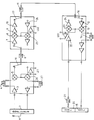
- Referring to the drawing there is shown a radio frequency circuit for a transmitter/receiver unit of a TDMA radio telephone system. The unit has an antenna 1 which is interfaced to receive and transmit channels via a duplexer 2.
- Considering the example of a GSM system where there is a transmit broadcast channel from 890 to 915 MHz and a receive broadcast channel from 935 MHz to 960 MHz, the receive channel of the RF circuit operates in this example as follows. The duplexer 2 feeds an amplifier 3 which applies signals via a band-pass filter 4 to a mixer 5. A local oscillator provides a frequency of 1324 MHz to give sidebands of 389 and 2259 MHz. A first IF filter 6 is switched at this time to be in the receive channel and is set to pass the 389 MHz sideband as the first intermediate frequency.
- The receive channel includes a further amplifier 7, a mixer 8 and two
further amplifier stages 9, 10. A second local oscillator LO2 supplies a frequency of 260 MHz to give sidebands of 129 and 649 MHz. A second IF filter 11 is switched at this time to the receive channel and is set to pass the 129 MHz sideband as the second IF. - A
further amplifier 12 supplies amixer 13 which is also provided by a third local oscillator LO3 with a frequency of 130 MHz. This produces sidebands of 1 and 259 MHz. A transconductance-C active filter 14 rejects the 259 MHz sideband, leaving the 1MHz signal to be fed to the low frequency digital demodulator (not shown) via an analogue todigital convertor 15. - In the transmit mode the circuit automatically switches over the channels and places the IF filters 6 and 11 in the transmit channel. Appropriate switches are shown symbolically at 16, 17, 18 and 19 but it is to be understood that switching is effected by biasing amplifiers in the channels which are physically permanently connected to the IF filters.
- 1 MHz signals from the low frequency digital modulator (not shown) are applied to the transmit channel via a digital to
analogue convertor 20 and alow stop filter 21 to anamplifier 22, amixer 23 and afurther amplifier 24. Inmixer 23 sidebands of 129 and 131 MHz are produced with the signal from local oscillator LO3. The 129 MHz signal is selected by filter 11. This and filter 6 are bidirectional SAW filters, operating similarly on signals passing in either direction. - The 129MHz IF is mixed with the LO2 signal in mixer after passing through an
amplifier 26. This produces sidebands of 389 and 131 MHz of which the 389 MHz signal is selected by filter 6 as the IF. This passes to amixer 26. Instead of the receive frequency of 1324 MHz the local oscillator LO1 is now switched to produce a transmit frequency of 1729 MHz. This produces sidebands of 890 and 2188 MHz. The 2118 MHz signal is rejected by afilter 27 to allow the broadcast frequency of 890 MHz to be transmitted. - A bandwidth of 300 KHz is required. The transmit requirements were to reject image frequencies and local oscillator leakage while passing the modulated transmit signal. The filter had to have a very carefully specified phase distortion in order that the global phase specification could be met at the antenna.
- The filter specification for receive was mainly dominated by the blocking and intermodulation specifications. The use of a low IF frequency for demodulation meant that image rejection was the hardest specification, this could not be achieved in one filter alone.
- The two requirements were then merged and played off against each other, the pass band requirement was set by the transmit requirement and the stop band was set by the receive requirements. The use of direct digital synthesis for modulation purposes also affected the pass band requirements.
- Another factor dictating the choice of the first intermediate frequency is the possibility to use the circuit with only minor modifications in the PCN system. Here the receive broadcast frequency is 1925 MHz and the transmit broadcast frequency is 1830 MHz. The same first IF of 389 MHz can be used, and thus the same SAW filters employed, if the receive and transmit LO1 frequencies are set to 1536 and 1441 MHz respectively.
Claims (10)
- A radio frequency circuit for a transmitter/receiver in a time division multiple access system, the circuit having a transmit channel, a receive channel, at least one intermediate frequency filter and means respcnsive to whether the circuit is transmitting or receiving to switch the or at least one of the filters to the transmit or receive channel, thereby allowing the filter or filters to be shared by the transmit and receive channels.
- A radio frequency circuit as claimed in Claim 1 wherein the or each switchable filter is bidirectional, having the capacity to filter signals passing through it in either direction.
- A radio frequency circuit as claimed in Claim 2 wherein the or each switchable filter is a SAW filter.
- A radio frequency circuit as claimed in any of the preceding claims wherein the switchable filters are physically connected to both the transmit and receive circuits and switching is effected by control voltages applied to components in the transmit and receive circuits to switch the circuits on and off alternatively.
- A radio frequency circuit as claimed in any of the preceding claims wherein there are two intermediate frequencies, the first (in the direction of the receive channel) being in the range 350 to 450 MHz.
- A radio frequency circuit as claimed in any of the preceding claims wherein the first intermediate frequency is in the range 380 to 420 MHz.
- A radio frequency circuit as claimed in any of the preceding claims wherein there are two intermediate frequencies, the second (in the direction of the receive channel) being in the range 80 to 160 MHz.
- A radio frequency circuit as claimed in Claim 7 wherein the second intermediate frequency is in the range 120 to 140 MHz.
- A radio frequency circuit as claimed in Claim 8 wherein there is provided a transconductance-C active filter in the receive channel for filtering the signal resulting from heterodyning the second intermediate frequency.
- A radio frequency circuit as claimed in any of the preceding claims wherein there is a first receiving stage/final transmitting stage which has a local oscillator automatically switchable on transmit/receive to change frequency so that the first receive intermediate frequency and final transmit intermediate frequency are the same.
Applications Claiming Priority (2)
| Application Number | Priority Date | Filing Date | Title |
|---|---|---|---|
| GB9223621A GB2272605B (en) | 1992-11-11 | 1992-11-11 | Radio frequency circuit for a time division multiple access system |
| GB9223621 | 1992-11-11 |
Publications (3)
| Publication Number | Publication Date |
|---|---|
| EP0597653A2 true EP0597653A2 (en) | 1994-05-18 |
| EP0597653A3 EP0597653A3 (en) | 1994-12-14 |
| EP0597653B1 EP0597653B1 (en) | 2002-03-06 |
Family
ID=10724903
Family Applications (1)
| Application Number | Title | Priority Date | Filing Date |
|---|---|---|---|
| EP93308904A Expired - Lifetime EP0597653B1 (en) | 1992-11-11 | 1993-11-08 | Radio frequency circuit for a time division multiple access system |
Country Status (4)
| Country | Link |
|---|---|
| US (1) | US5701594A (en) |
| EP (1) | EP0597653B1 (en) |
| DE (1) | DE69331653T2 (en) |
| GB (1) | GB2272605B (en) |
Cited By (8)
| Publication number | Priority date | Publication date | Assignee | Title |
|---|---|---|---|---|
| EP0653851A2 (en) * | 1993-11-12 | 1995-05-17 | Philips Patentverwaltung GmbH | Multiband radio transceiver |
| EP0845871A2 (en) * | 1996-11-20 | 1998-06-03 | Rockwell Science Center, Inc. | Intermediate frequency amplifier circuit for use in receive and transmit mode |
| CN1083645C (en) * | 1996-04-08 | 2002-04-24 | 松下电器产业株式会社 | Multiband mobile unit communication apparatus |
| EP1507334A1 (en) * | 2003-08-12 | 2005-02-16 | STMicroelectronics S.A. | Electronic component allowing the decoding of signals modulated by a digital quadrature modulation of a large number of orthogonal carriers |
| EP1881613A1 (en) | 1999-10-12 | 2008-01-23 | QUALCOMM Incorporated | Full-duplex transceiver with distributed duplexing function |
| US7446612B2 (en) | 2006-09-08 | 2008-11-04 | Skyworks Solutions, Inc. | Amplifier feedback and bias configuration |
| US7471154B2 (en) | 2006-08-08 | 2008-12-30 | Skyworks Solutions, Inc. | Bias circuit for maintaining high linearity at cutback power conditions |
| US7696826B2 (en) | 2006-12-04 | 2010-04-13 | Skyworks Solutions, Inc. | Temperature compensation of collector-voltage control RF amplifiers |
Families Citing this family (10)
| Publication number | Priority date | Publication date | Assignee | Title |
|---|---|---|---|---|
| US6177964B1 (en) * | 1997-08-01 | 2001-01-23 | Microtune, Inc. | Broadband integrated television tuner |
| JP3088338B2 (en) * | 1997-05-28 | 2000-09-18 | 埼玉日本電気株式会社 | Wireless telephone equipment |
| JP3389886B2 (en) * | 1999-06-09 | 2003-03-24 | 株式会社村田製作所 | High frequency circuit device and communication device |
| FI114591B (en) * | 2000-05-30 | 2004-11-15 | Nokia Corp | Procedure for realizing a transmitter / receiver and transmitter / receiver |
| TWI348269B (en) * | 2006-09-20 | 2011-09-01 | Mediatek Usa Inc | Transceiver and compound fileter |
| US8044742B2 (en) | 2009-03-11 | 2011-10-25 | Qualcomm Incorporated | Wideband phase modulator |
| US8260212B2 (en) * | 2009-05-19 | 2012-09-04 | Broadcom Corporation | Method and system for a reconfigurable filter that is utilized by a RF transmitter and a RF receiver which are integrated on a single substrate |
| US8588720B2 (en) * | 2009-12-15 | 2013-11-19 | Qualcomm Incorproated | Signal decimation techniques |
| US9000858B2 (en) | 2012-04-25 | 2015-04-07 | Qualcomm Incorporated | Ultra-wide band frequency modulator |
| TW201415794A (en) * | 2012-10-09 | 2014-04-16 | Issc Technologies Corp | A switchable filtering circuit and the operation method using the same |
Citations (7)
| Publication number | Priority date | Publication date | Assignee | Title |
|---|---|---|---|---|
| JPS5769939A (en) * | 1980-10-21 | 1982-04-30 | Nec Corp | Radio set |
| WO1985000481A1 (en) * | 1983-07-05 | 1985-01-31 | Motorola, Inc. | Simplex transceiver employing a common piezoelectric element for transmitting and receiving |
| JPS60107926A (en) * | 1983-11-16 | 1985-06-13 | Yaesu Musen Co Ltd | Radio communication equipment |
| EP0398688A2 (en) * | 1989-05-18 | 1990-11-22 | Nokia Mobile Phones Ltd. | Procedure for forming frequencies of a digital radio telephone |
| JPH03205908A (en) * | 1989-10-13 | 1991-09-09 | Hitachi Ltd | Surface acoustic wave device and communication equipment |
| EP0496498A2 (en) * | 1991-01-25 | 1992-07-29 | Matsushita Electric Industrial Co., Ltd. | Time-division duplex radio transceiver |
| EP0514200A2 (en) * | 1991-05-17 | 1992-11-19 | Nec Corporation | TDMA radio communication apparatus |
Family Cites Families (13)
| Publication number | Priority date | Publication date | Assignee | Title |
|---|---|---|---|---|
| NL302518A (en) * | 1962-12-31 | |||
| JPS524105A (en) * | 1975-06-27 | 1977-01-13 | Trio Kenwood Corp | Frequency synthesizer-method transmitter-receiver |
| JPS5324713A (en) * | 1976-08-20 | 1978-03-07 | Alps Electric Co Ltd | Ssb transceiver |
| US4137499A (en) * | 1977-04-27 | 1979-01-30 | Texas Instruments Incorporated | Signal strength measuring transceiver |
| JPS62274934A (en) * | 1986-05-23 | 1987-11-28 | Nec Corp | Transmitter-receiver |
| US5204972A (en) * | 1989-07-18 | 1993-04-20 | Nec Corporation | Arrangement for compensating for temperature dependent performance characteristics of surface acoustic wave filter |
| US5202652A (en) * | 1989-10-13 | 1993-04-13 | Hitachi, Ltd. | Surface acoustic wave filter device formed on a plurality of piezoelectric substrates |
| US5182477A (en) * | 1990-03-22 | 1993-01-26 | Silicon Systems, Inc. | Bipolar tunable transconductance element |
| JP2982354B2 (en) * | 1991-03-20 | 1999-11-22 | ソニー株式会社 | Transceiver |
| FI89845C (en) * | 1991-09-04 | 1993-11-25 | Nokia Mobile Phones Ltd | Connection for generating broadcast signal in a radio telephone |
| US5220557A (en) * | 1991-09-23 | 1993-06-15 | Hughes Aircraft Company | Multiple use digital transmitter/transceiver with time multiplexing |
| JP3122196B2 (en) * | 1991-10-31 | 2001-01-09 | 株式会社東芝 | Wireless communication device |
| US5355524A (en) * | 1992-01-21 | 1994-10-11 | Motorola, Inc. | Integrated radio receiver/transmitter structure |
-
1992
- 1992-11-11 GB GB9223621A patent/GB2272605B/en not_active Revoked
-
1993
- 1993-11-08 EP EP93308904A patent/EP0597653B1/en not_active Expired - Lifetime
- 1993-11-08 DE DE69331653T patent/DE69331653T2/en not_active Expired - Fee Related
- 1993-11-10 US US08/150,464 patent/US5701594A/en not_active Expired - Lifetime
Patent Citations (7)
| Publication number | Priority date | Publication date | Assignee | Title |
|---|---|---|---|---|
| JPS5769939A (en) * | 1980-10-21 | 1982-04-30 | Nec Corp | Radio set |
| WO1985000481A1 (en) * | 1983-07-05 | 1985-01-31 | Motorola, Inc. | Simplex transceiver employing a common piezoelectric element for transmitting and receiving |
| JPS60107926A (en) * | 1983-11-16 | 1985-06-13 | Yaesu Musen Co Ltd | Radio communication equipment |
| EP0398688A2 (en) * | 1989-05-18 | 1990-11-22 | Nokia Mobile Phones Ltd. | Procedure for forming frequencies of a digital radio telephone |
| JPH03205908A (en) * | 1989-10-13 | 1991-09-09 | Hitachi Ltd | Surface acoustic wave device and communication equipment |
| EP0496498A2 (en) * | 1991-01-25 | 1992-07-29 | Matsushita Electric Industrial Co., Ltd. | Time-division duplex radio transceiver |
| EP0514200A2 (en) * | 1991-05-17 | 1992-11-19 | Nec Corporation | TDMA radio communication apparatus |
Non-Patent Citations (4)
| Title |
|---|
| JEE JOURNAL OF ELECTRONIC ENGINEERING, vol.29, no.305, May 1992, TOKYO JP pages 54 - 57 KAZUO EDA 'Ultra-small SAW filter works in mobile communication' * |
| PATENT ABSTRACTS OF JAPAN vol. 15, no. 476 (E-1140) 4 December 1991 & JP-A-03 205 908 (HITACHI LTD) * |
| PATENT ABSTRACTS OF JAPAN vol. 6, no. 147 (E-123) 6 August 1982 & JP-A-57 069 939 (NEC CORP) * |
| PATENT ABSTRACTS OF JAPAN vol. 9, no. 258 (E-350) 16 October 1985 & JP-A-60 107 926 (YAESU MUSEN K.K.) * |
Cited By (13)
| Publication number | Priority date | Publication date | Assignee | Title |
|---|---|---|---|---|
| EP0653851A2 (en) * | 1993-11-12 | 1995-05-17 | Philips Patentverwaltung GmbH | Multiband radio transceiver |
| EP0653851A3 (en) * | 1993-11-12 | 1996-04-10 | Philips Patentverwaltung | Multiband radio transceiver. |
| CN1083645C (en) * | 1996-04-08 | 2002-04-24 | 松下电器产业株式会社 | Multiband mobile unit communication apparatus |
| EP0845871A2 (en) * | 1996-11-20 | 1998-06-03 | Rockwell Science Center, Inc. | Intermediate frequency amplifier circuit for use in receive and transmit mode |
| EP0845871A3 (en) * | 1996-11-20 | 2003-03-19 | Rockwell Science Center, Inc. | Intermediate frequency amplifier circuit for use in receive and transmit mode |
| EP1881613A1 (en) | 1999-10-12 | 2008-01-23 | QUALCOMM Incorporated | Full-duplex transceiver with distributed duplexing function |
| KR100798663B1 (en) | 1999-10-12 | 2008-01-28 | 퀄컴 인코포레이티드 | Full-duplex transceiver with distributed duplexing function |
| EP1221204B1 (en) * | 1999-10-12 | 2008-04-16 | QUALCOMM Incorporated | Full-duplex transceiver with distributed duplexing function |
| EP1507334A1 (en) * | 2003-08-12 | 2005-02-16 | STMicroelectronics S.A. | Electronic component allowing the decoding of signals modulated by a digital quadrature modulation of a large number of orthogonal carriers |
| US7474693B2 (en) | 2003-08-12 | 2009-01-06 | Stmicroelectronics, Sa | Electronic component notably for decoding signals modulated by a digital quadrature modulation over a large number of orthogonal carriers |
| US7471154B2 (en) | 2006-08-08 | 2008-12-30 | Skyworks Solutions, Inc. | Bias circuit for maintaining high linearity at cutback power conditions |
| US7446612B2 (en) | 2006-09-08 | 2008-11-04 | Skyworks Solutions, Inc. | Amplifier feedback and bias configuration |
| US7696826B2 (en) | 2006-12-04 | 2010-04-13 | Skyworks Solutions, Inc. | Temperature compensation of collector-voltage control RF amplifiers |
Also Published As
| Publication number | Publication date |
|---|---|
| EP0597653B1 (en) | 2002-03-06 |
| US5701594A (en) | 1997-12-23 |
| DE69331653D1 (en) | 2002-04-11 |
| GB2272605B (en) | 1996-11-27 |
| DE69331653T2 (en) | 2002-10-31 |
| GB9223621D0 (en) | 1992-12-23 |
| GB2272605A (en) | 1994-05-18 |
| EP0597653A3 (en) | 1994-12-14 |
Similar Documents
| Publication | Publication Date | Title |
|---|---|---|
| US5701594A (en) | Transmitter/receiver for a TDMA system using common IF SAW filter | |
| AU692642B2 (en) | Wide band radio-frequency converter having multiple use of intermediate frequency translators | |
| US6130897A (en) | Time division multiple access FDD/TDD dual mode radio and a time division multiple access TDD dual band system | |
| US6175746B1 (en) | Multiband mobile unit communication apparatus | |
| US5640686A (en) | Radio communication device capable of communication in a plurality of communication systems | |
| US6584304B1 (en) | Switchable wide band receiver front end for a multiband receiver | |
| US5963856A (en) | Wireless receiver including tunable RF bandpass filter | |
| EP0813312B1 (en) | Multiband mobile unit communication apparatus | |
| US5852784A (en) | Multiband mobile unit communication apparatus | |
| US5995815A (en) | Multiple band receiver | |
| US6269253B1 (en) | Multi-mode wireless communication system | |
| JPH09261106A (en) | Mobile radio equipment operated for plural frequency bands | |
| WO1998037629A1 (en) | Receiver if system with active filters | |
| US6091963A (en) | Multi-frequency band receiver for RF signal | |
| US6922554B2 (en) | Method for implementing a transceiver and a transceiver | |
| US5307378A (en) | Digital radio communication apparatus | |
| CA2456658C (en) | A mixer circuit with image frequency rejection, in particular for an rf receiver with zero or low intermediate frequency | |
| JPH07231273A (en) | Tuner for receiving satellite broadcast | |
| JPH09261104A (en) | Mobile radio equipment operated in plural modes | |
| KR100212066B1 (en) | Apparatus and method for controlling the low frequency attenuation in the wireless communication system | |
| KR100212054B1 (en) | Transceiver circuits with common used inter frequency | |
| JPH09275351A (en) | Plural-mode mobile radio equipment | |
| JPS63266932A (en) | Transmitter-receiver | |
| JPS62139419A (en) | Car radio circuit | |
| JPH05284055A (en) | Receiver |
Legal Events
| Date | Code | Title | Description |
|---|---|---|---|
| PUAI | Public reference made under article 153(3) epc to a published international application that has entered the european phase |
Free format text: ORIGINAL CODE: 0009012 |
|
| AK | Designated contracting states |
Kind code of ref document: A2 Designated state(s): DE FR GB IT |
|
| PUAL | Search report despatched |
Free format text: ORIGINAL CODE: 0009013 |
|
| AK | Designated contracting states |
Kind code of ref document: A3 Designated state(s): DE ES FR GB IT SE |
|
| 17P | Request for examination filed |
Effective date: 19950614 |
|
| 17Q | First examination report despatched |
Effective date: 19991018 |
|
| GRAG | Despatch of communication of intention to grant |
Free format text: ORIGINAL CODE: EPIDOS AGRA |
|
| GRAG | Despatch of communication of intention to grant |
Free format text: ORIGINAL CODE: EPIDOS AGRA |
|
| GRAH | Despatch of communication of intention to grant a patent |
Free format text: ORIGINAL CODE: EPIDOS IGRA |
|
| RBV | Designated contracting states (corrected) |
Designated state(s): DE FR GB IT |
|
| GRAH | Despatch of communication of intention to grant a patent |
Free format text: ORIGINAL CODE: EPIDOS IGRA |
|
| REG | Reference to a national code |
Ref country code: GB Ref legal event code: IF02 |
|
| GRAA | (expected) grant |
Free format text: ORIGINAL CODE: 0009210 |
|
| AK | Designated contracting states |
Kind code of ref document: B1 Designated state(s): DE FR GB IT |
|
| RAP2 | Party data changed (patent owner data changed or rights of a patent transferred) |
Owner name: NOKIA CORPORATION |
|
| REF | Corresponds to: |
Ref document number: 69331653 Country of ref document: DE Date of ref document: 20020411 |
|
| REG | Reference to a national code |
Ref country code: GB Ref legal event code: 732E |
|
| ET | Fr: translation filed | ||
| PGFP | Annual fee paid to national office [announced via postgrant information from national office to epo] |
Ref country code: GB Payment date: 20021106 Year of fee payment: 10 |
|
| PGFP | Annual fee paid to national office [announced via postgrant information from national office to epo] |
Ref country code: FR Payment date: 20021108 Year of fee payment: 10 |
|
| PLBE | No opposition filed within time limit |
Free format text: ORIGINAL CODE: 0009261 |
|
| STAA | Information on the status of an ep patent application or granted ep patent |
Free format text: STATUS: NO OPPOSITION FILED WITHIN TIME LIMIT |
|
| 26N | No opposition filed |
Effective date: 20021209 |
|
| PG25 | Lapsed in a contracting state [announced via postgrant information from national office to epo] |
Ref country code: DE Free format text: LAPSE BECAUSE OF NON-PAYMENT OF DUE FEES Effective date: 20030603 |
|
| PG25 | Lapsed in a contracting state [announced via postgrant information from national office to epo] |
Ref country code: GB Free format text: LAPSE BECAUSE OF NON-PAYMENT OF DUE FEES Effective date: 20031108 |
|
| GBPC | Gb: european patent ceased through non-payment of renewal fee |
Effective date: 20031108 |
|
| PG25 | Lapsed in a contracting state [announced via postgrant information from national office to epo] |
Ref country code: FR Free format text: LAPSE BECAUSE OF NON-PAYMENT OF DUE FEES Effective date: 20040730 |
|
| REG | Reference to a national code |
Ref country code: FR Ref legal event code: ST |
|
| PG25 | Lapsed in a contracting state [announced via postgrant information from national office to epo] |
Ref country code: IT Free format text: LAPSE BECAUSE OF NON-PAYMENT OF DUE FEES;WARNING: LAPSES OF ITALIAN PATENTS WITH EFFECTIVE DATE BEFORE 2007 MAY HAVE OCCURRED AT ANY TIME BEFORE 2007. THE CORRECT EFFECTIVE DATE MAY BE DIFFERENT FROM THE ONE RECORDED. Effective date: 20051108 |