EP0594971A1 - High impedance output driver stage and method therefor - Google Patents
High impedance output driver stage and method therefor Download PDFInfo
- Publication number
- EP0594971A1 EP0594971A1 EP93113641A EP93113641A EP0594971A1 EP 0594971 A1 EP0594971 A1 EP 0594971A1 EP 93113641 A EP93113641 A EP 93113641A EP 93113641 A EP93113641 A EP 93113641A EP 0594971 A1 EP0594971 A1 EP 0594971A1
- Authority
- EP
- European Patent Office
- Prior art keywords
- output
- current
- stage
- input
- transistor
- Prior art date
- Legal status (The legal status is an assumption and is not a legal conclusion. Google has not performed a legal analysis and makes no representation as to the accuracy of the status listed.)
- Withdrawn
Links
Images

Classifications
-
- H—ELECTRICITY
- H03—ELECTRONIC CIRCUITRY
- H03F—AMPLIFIERS
- H03F1/00—Details of amplifiers with only discharge tubes, only semiconductor devices or only unspecified devices as amplifying elements
- H03F1/56—Modifications of input or output impedances, not otherwise provided for
Definitions
- This invention relates, in general, to amplifiers, and more particularly to circuits for buffering a gain stage from an output stage.
- a common form of an amplifier comprises an input gain stage (or first gain stage), a second gain stage, and an output stage.
- the second gain stage is often combined with the output stage.
- the output stage is defined as the circuitry which drives a load external to the amplifier.
- Each amplifier stage interacts with the other amplifier stages. This interaction affects performance of each amplifier stage as well as the overall performance of the amplifier.
- Design of an amplifier in part, is the melding of each amplifier stage, which in some cases means compromising performance of a particular stage for the benefit of amplifier performance in total. Of particular concern is the effect of the output stage on the second gain stage, or more generally, a gain stage coupled to a high drive stage.
- the second gain stage provides an amplified voltage signal which is coupled to the output stage.
- the output stage generally does not have voltage gain but provides current drive to a load external to the amplifier.
- the output stage may be required to sink or source a current of significant magnitude depending on the external load.
- the output stage may present a low impedance load to the second gain stage.
- the second gain stage performance may be severely degraded by the low impedance load presented by the output stage for some circuit configurations.
- One approach to solve this problem is to add a buffer stage between the second gain stage and the output stage.
- the buffer stage presents a high impedance load to the second gain stage while having the capability to drive a low impedance load (such as the input of an output stage).
- a first circuit configuration of a buffer stage used between the second gain stage and an output stage is a bipolar transistor Darlington configuration.
- Darlington configured bipolar transistors have high current gain and high input impedance, both parameters are critical for the design of a good buffer stage.
- the Darlington configured buffer stage has been used successfully in an operational amplifier such as the MC33077 manufactured by Motorola Inc..
- the Darlington configured buffer stage is not without problems which limit its applications in many amplifier designs.
- the main problem with the Darlington configured buffer stage is that it affects the frequency response of the amplifier by adding phase shift which can cause amplifier instability when using feedback.
- the added phase shift contributed by the Darlington configured buffer stage is enough to limit amplifier performance or complicate the amplifier compensation scheme to the point where alternative circuit approaches are preferential to the Darlington configuration.
- a second circuit configuration commonly used throughout the industry is a PNP bipolar transistor coupled to a current source.
- the PNP bipolar transistor is coupled to a gain stage in a voltage follower configuration for buffering the gain stage from a high drive stage.
- An example of this type of stage is in a MC33174 operational amplifier manufactured by Motorola Inc..
- PNP transistors in many semiconductor process flows have inferior performance characteristics than NPN transistors fabricated in the same process. This is the case for the MC33174 operational amplifier which must add additional circuitry to account for the performance deficiencies of using PNP transistors.
- a PNP based buffer stage adds phase shift to the amplifier loop, thus complicating amplifier compensation.
- Feed-forward capacitors are sometimes used to bypass the PNP transistor for high frequency signals due to the slow response time of the PNP transistor (adding more components to the amplifier design). If the PNP buffer stage is coupled to a differential gain stage, base current from the PNP buffer must be taken into account, otherwise, an offset could be induced into the amplifier. This is resolved by adding a dummy stage which mimics the base current from the PNP buffer but at the cost of more circuitry.
- a buffer stage which buffers a gain stage from an output stage (or high drive stage).
- the buffer stage should present a high impedance load to the gain stage, have the capability to drive a low impedance high drive stage, add minimal phase shift to the circuit, and keep component counts low.
- a high impedance output stage comprises an output stage, a current sense circuit, and a current source circuit.
- the output stage has an input and an output.
- the output stage is responsive to an input current and generates an output current.
- the current sense circuit senses input or output current of the output stage and generates a sense current proportional to the input current of the output stage.
- the current source circuit has an input which is responsive to the sense current from the current sense circuit and has an output coupled to the input of the output stage.
- the current source circuit outputs a current substantially equal to the input current of the output stage.
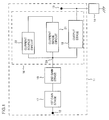
- FIG. 1 is a block diagram of an amplifier having a high impedance output stage in accordance with the present invention.
- An amplifier is ideal for illustrating the interaction between a gain stage coupled to an output stage (or high drive stage).
- a gain stage typically, is designed to amplify a voltage signal by a predetermined gain. This contrasts greatly to an output stage, the output stage is designed to drive a load external to the amplifier and typically does not have voltage gain.
- the load or impedance presented by the output stage to the gain stage can impact performance of the gain stage. For example, the impedance of an output stage for some types of circuits varies with output current (of the output stage). Under high drive conditions the output stage can present a low impedance load to the gain stage. The increased loading of the gain stage under high drive conditions can affect amplifier characteristics such as voltage gain, voltage offset or stability.
- a common approach used by those skilled in the art is to add a buffer stage between the gain stage and the output stage to alleviate the loading problem.
- the buffer stage presents a high impedance load to the gain stage yet can drive a low impedance load (output stage).
- the main problem with the buffer stage is that it affects frequency response and stability of the amplifier. It is placed directly in the gain path through the amplifier and adds phase shift which reduces amplifier stability when feedback is used. Additional circuitry can be added to the buffer stage to compensate for these deficiencies but it will increase silicon area and circuit complexity.
- a solution to the problem of gain stage loading is to directly couple the gain stage to the output stage (thus eliminating phase shift added by buffer stages) and using a circuit (peripheral to the gain path) which senses and supplies an "appropriate current'' to the output stage thereby eliminating the gain stage from sourcing any significant current.
- the output stage does not load the gain stage.
- An amplifier 11 has an input 12 for receiving an input signal to be amplified and an output 13.
- Amplifier 11 has two gain stages, a first gain stage 17 and a second gain stage 18.
- First gain stage 17 has an input coupled to amplifier input 12 and an output coupled to an input of second gain stage 18.
- An output of second gain stage 18 is coupled to a node 23.
- An output stage 19 for driving a load 14 has an input coupled to node 23 and an output coupled to amplifier output 13. Note that the input of output stage 19 is directly coupled to the output of second gain stage 18 by node 23, thus, nothing is inserted in the gain path through amplifier 11 to add additional phase shift.
- the high impedance output driver stage 16 comprises output stage 19, current sense circuit 21, and current source circuit 22.
- Current sense circuit 21 serves as a means for sensing current.
- Current sense circuit 21 has an input coupled to node 23 for sensing a current of output stage 19 (either input current or output current of the output stage) and an output.
- Current sense circuit 21 generates a current proportional to the input current to output stage 19.
- Current source circuit 22 serves as a means for sourcing current.
- Current source circuit 22 has an input coupled to the output of current sense circuit 21 and an output coupled to node 23.
- Current source circuit 22 is responsive to the current output from current senses circuit 21 and generates a current "substantially equal" to the input current of output stage 19.
- second gain stage 18 does not supply any current to output stage 19 if the current supplied by current source circuit 22 is exactly equal to the current needed by output stage 19, thus output stage 19 would appear as an infinite impedance (open circuit) to second gain stage 18.
- Both second gain stage 18 and output stage 19 can be optimized to perform their appropriate tasks without compromising overall performance of amplifier 11 since the impedance presented by output stage 19 does not impact second gain stage 18 performance.
- High impedance output driver stage 16 is an active circuit which first senses current of output stage 19 then supplies input current to output stage 19. In other words, it transitions or changes to the immediate input current needs of output stage 19.
- current source circuit 22 is not allowed to supply a current greater than output stage 19 needs. A larger current could result in the latch up of amplifier 11. This problem is alleviated by adjusting current sense circuit 21 and current source circuit 22 to insure over all conditions (temperature, process, device matching, voltage, etc.) that a current equal to or less than the input current of output stage 19 is delivered by current source circuit 22. Any current not sourced by current source circuit 22 to the input of output stage 19 must be sourced by second gain stage 18 but does not impact performance significantly.
- FIG. 2 is a schematic of an embodiment of a high impedance output driver stage in an amplifier.
- An amplifier 30 is a simplified design of an integrated circuit operational amplifier illustrating functioning circuits corresponding to the blocks of FIG. 1.
- Amplifier 30 comprises a first gain stage 31, a second gain stage 32, an output stage 33, a current sense circuit 34, and a current source circuit 36.
- First gain stage 31 is a differential gain stage having a first input 37, a second input 38, a first output, and a second output.
- First input 37 and second input 38 are inputs of amplifier 30.
- a difference in voltage potential between first input 37 and second input 38 generates a differential input voltage signal which is amplified by first gain stage 31.
- the amplified differential signal is coupled to a second gain stage 32 through the first output and second output of first gain stage 31.
- Second gain stage 32 is an amplification stage having high voltage gain.
- the amplified differential signal coupled to second gain stage 32 is further amplified and converted to a single ended (non-differential) voltage signal.
- the schematic diagram of second gain stage 32 illustrates common features of an amplification stage which benefit significantly through the use of this invention.
- Other types of gain stage could be used equally well with the a high impedance output driver stage 61.
- a current source 39 is coupled to a terminal of power supply 42 and has an output.
- a PNP transistor 44 has an emitter coupled to the output of current source 39, a base coupled to a D.C. bias voltage Vbias, and a collector coupled to a node 47.
- a diode 49 has an anode coupled to node 47 and a cathode.
- a NPN transistor 52 has a collector coupled to the cathode of diode 49, a base coupled to a node 54, and an emitter coupled to the first output of first gain stage 31.
- the emitter of transistor 52 is an input of second gain stage 32.
- a NPN transistor 53 has a collector coupled to node 54, a base coupled to node 54, and an emitter coupled to the second output of of first gain stage 31.
- the emitter of transistor 53 is an input of second gain stage 32.
- a NPN transistor 51 has a collector coupled to a node 48, a base coupled to node 47, and an emitter coupled to node 54.
- a PNP transistor 46 has a collector coupled to node 48, a base coupled to the D.C. bias voltage Vbias, and an emitter.
- a current source 41 is coupled to the terminal of power supply 42 and has an output coupled to the emitter of PNP transistor 46.
- a NPN transistor 55 has a collector coupled to the terminal of power supply 42, a base coupled to the emitter of PNP transistor 44, and an emitter.
- a NPN transistor 56 has a collector coupled to the emitter of NPN transistor 55, a base coupled to node 48, and a emitter coupled to a node 58.
- the emitter of transistor 56 is an output of second gain stage 32.
- a current source 57 completes second gain stage 32 and is coupled to a terminal of power supply 59 and has an output coupled to node 58.
- second gain stage 32 Operation of second gain stage 32 is quite simple and is well known by those skilled in the art.
- Current sources 39 and 41 output substantially equal currents.
- second gain stage 32 is in a balanced state when the first and second outputs of first gain stage 31 are at equal voltages.
- a condition of this balanced state is that collector current output by transistor 46 is approximately the same as collector current into transistor 51.
- a voltage difference between the first and second outputs of first gain stage 31 will generate a difference current at node 48.
- the difference current is incrementally positive or negative and results from a difference in current between transistor 46 source current and transistor 51 sink current.
- the difference current is created, in part, by a current mirror circuit comprising transistors 51, 52, and 53, and diode 49.
- Transistor 56 is in a voltage follower configuration and acts as a buffer. An incremental positive (or enabling) difference current into the base of transistor 56 will generate a positive incremental current into output stage 33. Similarly, an incremental negative (or disabling) difference current into the base of transistor 56 will reduce current output of transistor 56 thus generating an incremental negative current. In other words, the voltage at node 58 rises and falls depending on the difference current into the base of transistor 56.
- Vbias is a D.C. voltage coupled to the base of transistor 44 and 46 to bias the transistors. Vbias is chosen to minimize performance impacts on other circuitry in second gain stage 32.
- second gain stage 32 it would be beneficial to second gain stage 32 if any loading on node 58 by output stage 33 would not affect the impedance at node 48.
- the gain of second gain stage 32 is directly related to the impedance at node 48.
- a high impedance at node 48 over varying conditions (voltage, processing, temperature, device characteristics, etc.) would insure a high voltage gain for second gain stage 32.
- output stage 33 can severely impact performance of second gain stage 32.
- the resistance looking into the base of transistor 56 is approximately the transistor current gain (or beta) x (emitter resistance of transistor 56 + resistance at node 58).
- the input resistance of transistor 56 can be the dominant resistance at node 48 which determines the gain of second gain stage 32.
- Output stage 33 presents an impedance at node 58 which can vary by orders of magnitude depending on the operating conditions and output loading. This variability will cause the input resistance of transistor 56 to also vary (dependent on operating conditions) which is not conducive to a stable amplifier design. It is typically resolved by use of a buffer stage (as mentioned previously) at the expense of added circuit complexity and increased phase shift. Other secondary problems can also be exaggerated by a low impedance at node 58. These secondary problems can range from increased voltage offset due to imbalanced loading on second gain stage 32 to operation problems at the temperature extremes. Problems of this type can be resolved by limiting the impact of output stage 33 on second gain stage 32 and optimization of each circuit.
- Output stage 33 is a simplified driver stage circuit comprising a current source 62 and a NPN transistor 63 for driving a load external to amplifier 30.
- Current source 62 is coupled to the terminal of power supply 42 and has an output coupled to an amplifier output 64.
- Transistor 63 has a base, collector, and emitter corresponding to a control input, a first conductive terminal, and a second conductive terminal, respectively.
- Transistor 63 has the collector coupled to amplifier output 64, the base coupled to node 58, and the emitter coupled to the terminal of power supply 59.
- transistor 63 is a high current device which has the potential to degrade performance of second gain stage 32 by lowering the impedance at node 48.
- a current sense circuit 34 comprises a NPN transistor 66.
- Transistor 66 has a base, collector, and emitter corresponding to a control input, a first conductive terminal, and a second conductive terminal, respectively.
- Transistor 66 has the collector coupled to a node 67, the base coupled to node 58, and the emitter coupled to the terminal of power supply 59.
- the emitter area of transistor 66 is a predetermined ratio of the emitter area of transistor 63.
- Transistor 66 will have a collector current related by the predetermined emitter area ratio to a collector current of transistor 63 because the base-emitter junction of transistor 66 is biased identically to the base-emitter junction of transistor 63.
- the emitter areas of transistors 66 and 63 are ratioed as accurate as possible. For illustration purposes assume that the emitter area of transistor 63 is 18 times larger than the emitter area of transistor 66.
- Current source circuit 36 comprises a NPN transistor 68, a diode 69, a PNP transistor 71, and a PNP transistor 72.
- Current source circuit 36 is responsive to the collector current of transistor 66 (which is proportional to the current in transistor 63) and outputs a current substantially equal to the combined base currents of transistors 66 and 63, thus reducing drive requirements of transistor 56.
- Transistor 68 has a base, collector, and emitter corresponding to a control input, a first conductive terminal, and a second conductive terminal, respectively.
- Transistor 68 has the collector coupled to the terminal of power supply 42, the base coupled to a node 73, and the emitter coupled to the node 67.
- Diode 69 has an anode and a cathode corresponding to a first terminal and a second terminal, respectively.
- Diode 69 has the anode coupled to the terminal of power supply 42 and the cathode coupled to node 73.
- Transistor 71 has a base, collector, and emitter corresponding to a control input, a first conductive terminal, and a second conductive terminal, respectively.
- Transistor 71 has the base coupled to node 73 and the emitter coupled to the terminal of power supply 42.
- Transistor 72 has a base, collector, and emitter corresponding to a control input, a first conductive terminal, and a second conductive terminal, respectively.
- Transistor 72 completes current source circuit 36 and has the collector coupled to node 58, the base coupled to node 67, and the emitter coupled to the collector of transistor 71.
- the collector current of transistor 66 is 1/18 of the collector current of transistor 63.
- current source circuit 36 generates 19 times the base current of transistor 66 thereby supplying base current for both transistor 66 and transistor 63.
- transistor 68 is identical to transistor 66 and is biased with the collector current of transistor 66.
- Transistor 68 is biased to generate a base current which approximates the base current into transistor 66.
- the base current of transistor 68 is increased nineteenfold by the combination of diode 69 and transistor 71 which acts as a current multiplication circuit.
- diode 69 and transistor 71 is made from a split collector lateral PNP transistor.
- the split collector lateral PNP transistor has the collector area ratioed 19 to one where transistor 71 compromises the portion of the device with 19 times the collector area and diode 69 is formed by coupling the single collector area back to the base region of the split collector PNP.
- the current through diode 69 (which approximates the base current of transistor 66) is multiplied 19 times by the ratio of collector area of transistor 71 to diode 69, thus the collector current of transistor 71 is approximately nineteen times the base current of transistor 66.
- transistor 72 is a cascode device placed in series with transistor 71 to reduce the voltage drop from collector to emitter of transistor 71.
- High impedance output driver stage 61 comprises output stage 33, current sense circuit 34, and current source circuit 36.
- Current sense circuit 34 and current source circuit 36 actively senses current of output stage 33 and sources a current to output stage 33.
- current source circuit 36 sources a current approximately 19 times the base current of transistor 66 which is sufficient to source base current for transistors 66 and 63. The magnitude of the current which current source circuit 36 sources will vary dependent on the needs of transistor 63.
- transistor 56 of second gain stage 32 sources no (zero) current to high impedance output driver stage 61.
- high impedance output driver stage 61 appears as an infinite impedance (under this ideal condition) thereby eliminating any restrictions placed on the design of second gain stage 32 due to interactions with output stage 33.
- high impedance output driver stage 61 is designed to "always" deliver less current than is needed by transistors 66 and 63. This is critical to prevent a latchup condition and must occur for all operating conditions (temperature, voltage, process, etc.) of amplifier 30.
- transistor 56 of second output stage 32 does source current to high impedance stage 61 albeit a significantly smaller current than it would supply driving output stage 33 without current sense circuit 34 and current source circuit 36.
- An important feature of high impedance output driver stage 61 is that no added components other than output stage 33 are in the gain path of amplifier 30 which minimizes complexity of the amplifier compensation scheme.
- High impedance output driver stage 61 not only maximizes frequency response of amplifier 30 by not adding any significant phase shift but also allows individual optimization of both second gain stage 32 and output stage 33 because of limited interaction between each other. Stability in sensing and sourcing current over all operating conditions is insured by using device matching to sense current in output stage 33 and also to generate the "reference base current" into transistor 68 thereby tracking over varying conditions. Secondary problems can also be reduced through optimization of the circuitry.
- FIG.2 illustrates one embodiment of high impedance output driver stage 61.
- current is sourced to output stage 33.
- current sense circuit 34 and current source circuit 36 can be designed to "source” or “sink” current (or both) dependent on the application.
- gain stage circuits and output stage circuits may vary significantly in form from that described in FIG. 2. Because of these variations in circuit design, current sense circuit 34 and current source circuit 36 must be designed for the specific application and may take many different forms, although functionally it will perform similarly to the embodiment described.
Abstract
A high impedance output driver stage (16) for reducing loading on a gain stage (18) which drives an output stage (19). The output stage (19) is responsive to an input current. A current sense circuit (21) senses current of output stage (19). The current sense circuit (21) outputs a current proportional to the current sensed in the output stage (19). A current source circuit (22) is responsive to the current output by the current sense circuit (21) and outputs a current substantially equal to the input current of the output stage (19) thereby reducing loading on the gain stage (18).
Description
- This invention relates, in general, to amplifiers, and more particularly to circuits for buffering a gain stage from an output stage.
- A common form of an amplifier comprises an input gain stage (or first gain stage), a second gain stage, and an output stage. Those skilled in the art will also know that the second gain stage is often combined with the output stage. For this case, the output stage is defined as the circuitry which drives a load external to the amplifier. Each amplifier stage interacts with the other amplifier stages. This interaction affects performance of each amplifier stage as well as the overall performance of the amplifier. Design of an amplifier, in part, is the melding of each amplifier stage, which in some cases means compromising performance of a particular stage for the benefit of amplifier performance in total. Of particular concern is the effect of the output stage on the second gain stage, or more generally, a gain stage coupled to a high drive stage.
- For example, the second gain stage provides an amplified voltage signal which is coupled to the output stage. The output stage generally does not have voltage gain but provides current drive to a load external to the amplifier. The output stage may be required to sink or source a current of significant magnitude depending on the external load. Under high drive conditions the output stage may present a low impedance load to the second gain stage. The second gain stage performance may be severely degraded by the low impedance load presented by the output stage for some circuit configurations. One approach to solve this problem is to add a buffer stage between the second gain stage and the output stage. Ideally, the buffer stage presents a high impedance load to the second gain stage while having the capability to drive a low impedance load (such as the input of an output stage).
- A first circuit configuration of a buffer stage used between the second gain stage and an output stage is a bipolar transistor Darlington configuration. Those skilled in the art know that Darlington configured bipolar transistors have high current gain and high input impedance, both parameters are critical for the design of a good buffer stage. The Darlington configured buffer stage has been used successfully in an operational amplifier such as the MC33077 manufactured by Motorola Inc.. The Darlington configured buffer stage is not without problems which limit its applications in many amplifier designs. The main problem with the Darlington configured buffer stage is that it affects the frequency response of the amplifier by adding phase shift which can cause amplifier instability when using feedback. The added phase shift contributed by the Darlington configured buffer stage is enough to limit amplifier performance or complicate the amplifier compensation scheme to the point where alternative circuit approaches are preferential to the Darlington configuration.
- A second circuit configuration commonly used throughout the industry is a PNP bipolar transistor coupled to a current source. The PNP bipolar transistor is coupled to a gain stage in a voltage follower configuration for buffering the gain stage from a high drive stage. An example of this type of stage is in a MC33174 operational amplifier manufactured by Motorola Inc.. PNP transistors in many semiconductor process flows have inferior performance characteristics than NPN transistors fabricated in the same process. This is the case for the MC33174 operational amplifier which must add additional circuitry to account for the performance deficiencies of using PNP transistors. Like the Darlington configured transistors a PNP based buffer stage adds phase shift to the amplifier loop, thus complicating amplifier compensation. Feed-forward capacitors are sometimes used to bypass the PNP transistor for high frequency signals due to the slow response time of the PNP transistor (adding more components to the amplifier design). If the PNP buffer stage is coupled to a differential gain stage, base current from the PNP buffer must be taken into account, otherwise, an offset could be induced into the amplifier. This is resolved by adding a dummy stage which mimics the base current from the PNP buffer but at the cost of more circuitry.
- It would be of great benefit if a buffer stage could be developed which buffers a gain stage from an output stage (or high drive stage). The buffer stage should present a high impedance load to the gain stage, have the capability to drive a low impedance high drive stage, add minimal phase shift to the circuit, and keep component counts low.
- Briefly stated, this invention provides an output stage having a high input impedance. A high impedance output stage comprises an output stage, a current sense circuit, and a current source circuit. The output stage has an input and an output. The output stage is responsive to an input current and generates an output current. The current sense circuit senses input or output current of the output stage and generates a sense current proportional to the input current of the output stage. The current source circuit has an input which is responsive to the sense current from the current sense circuit and has an output coupled to the input of the output stage. The current source circuit outputs a current substantially equal to the input current of the output stage.
-
- FIG. 1 is a block diagram of an amplifier in accordance with the present invention; and
- FIG. 2 is schematic diagram of an embodiment of an amplifier in accordance with the present invention.
- FIG. 1 is a block diagram of an amplifier having a high impedance output stage in accordance with the present invention.
- An amplifier is ideal for illustrating the interaction between a gain stage coupled to an output stage (or high drive stage). A gain stage, typically, is designed to amplify a voltage signal by a predetermined gain. This contrasts greatly to an output stage, the output stage is designed to drive a load external to the amplifier and typically does not have voltage gain. The load or impedance presented by the output stage to the gain stage can impact performance of the gain stage. For example, the impedance of an output stage for some types of circuits varies with output current (of the output stage). Under high drive conditions the output stage can present a low impedance load to the gain stage. The increased loading of the gain stage under high drive conditions can affect amplifier characteristics such as voltage gain, voltage offset or stability. The design of a gain stage with stable characteristics under a wide variation of loading conditions is difficult to achieve at best. A common approach used by those skilled in the art is to add a buffer stage between the gain stage and the output stage to alleviate the loading problem. The buffer stage presents a high impedance load to the gain stage yet can drive a low impedance load (output stage). The main problem with the buffer stage is that it affects frequency response and stability of the amplifier. It is placed directly in the gain path through the amplifier and adds phase shift which reduces amplifier stability when feedback is used. Additional circuitry can be added to the buffer stage to compensate for these deficiencies but it will increase silicon area and circuit complexity. A solution to the problem of gain stage loading is to directly couple the gain stage to the output stage (thus eliminating phase shift added by buffer stages) and using a circuit (peripheral to the gain path) which senses and supplies an "appropriate current'' to the output stage thereby eliminating the gain stage from sourcing any significant current. Thus, the output stage does not load the gain stage. This approach is the basis for creating a high impedance
output driver stage 16. - An
amplifier 11 has aninput 12 for receiving an input signal to be amplified and anoutput 13.Amplifier 11 has two gain stages, afirst gain stage 17 and asecond gain stage 18. The benefits of using two stages of gain in amplifier design (such as an integrated operational amplifier) is well known in the art.First gain stage 17 has an input coupled toamplifier input 12 and an output coupled to an input ofsecond gain stage 18. An output ofsecond gain stage 18 is coupled to anode 23. Anoutput stage 19 for driving aload 14 has an input coupled tonode 23 and an output coupled toamplifier output 13. Note that the input ofoutput stage 19 is directly coupled to the output ofsecond gain stage 18 bynode 23, thus, nothing is inserted in the gain path throughamplifier 11 to add additional phase shift. - The high impedance
output driver stage 16 comprisesoutput stage 19,current sense circuit 21, andcurrent source circuit 22.Current sense circuit 21 serves as a means for sensing current.Current sense circuit 21 has an input coupled tonode 23 for sensing a current of output stage 19 (either input current or output current of the output stage) and an output.Current sense circuit 21 generates a current proportional to the input current tooutput stage 19.Current source circuit 22 serves as a means for sourcing current.Current source circuit 22 has an input coupled to the output ofcurrent sense circuit 21 and an output coupled tonode 23.Current source circuit 22 is responsive to the current output fromcurrent senses circuit 21 and generates a current "substantially equal" to the input current ofoutput stage 19. Ideally,second gain stage 18 does not supply any current tooutput stage 19 if the current supplied bycurrent source circuit 22 is exactly equal to the current needed byoutput stage 19, thusoutput stage 19 would appear as an infinite impedance (open circuit) tosecond gain stage 18. Bothsecond gain stage 18 andoutput stage 19 can be optimized to perform their appropriate tasks without compromising overall performance ofamplifier 11 since the impedance presented byoutput stage 19 does not impactsecond gain stage 18 performance. - High impedance
output driver stage 16 is an active circuit which first senses current ofoutput stage 19 then supplies input current tooutput stage 19. In other words, it transitions or changes to the immediate input current needs ofoutput stage 19. In the preferred embodiment,current source circuit 22 is not allowed to supply a current greater thanoutput stage 19 needs. A larger current could result in the latch up ofamplifier 11. This problem is alleviated by adjustingcurrent sense circuit 21 andcurrent source circuit 22 to insure over all conditions (temperature, process, device matching, voltage, etc.) that a current equal to or less than the input current ofoutput stage 19 is delivered bycurrent source circuit 22. Any current not sourced bycurrent source circuit 22 to the input ofoutput stage 19 must be sourced bysecond gain stage 18 but does not impact performance significantly. It should be noted that current flow direction into or out of blocks ofamplifier 11 is not implied in the description cited above, only thatcurrent source circuit 22 sources a current (positive or negative) to enableoutput stage 19 such thatsecond gain stage 18 does not have to source the input current (positive or negative) ofoutput stage 19. - FIG. 2 is a schematic of an embodiment of a high impedance output driver stage in an amplifier.
- An
amplifier 30 is a simplified design of an integrated circuit operational amplifier illustrating functioning circuits corresponding to the blocks of FIG. 1.Amplifier 30 comprises afirst gain stage 31, asecond gain stage 32, an output stage 33, acurrent sense circuit 34, and acurrent source circuit 36. -
First gain stage 31 is a differential gain stage having afirst input 37, asecond input 38, a first output, and a second output.First input 37 andsecond input 38 are inputs ofamplifier 30. A difference in voltage potential betweenfirst input 37 andsecond input 38 generates a differential input voltage signal which is amplified byfirst gain stage 31. The amplified differential signal is coupled to asecond gain stage 32 through the first output and second output offirst gain stage 31. -
Second gain stage 32 is an amplification stage having high voltage gain. The amplified differential signal coupled tosecond gain stage 32 is further amplified and converted to a single ended (non-differential) voltage signal. Although simplified, the schematic diagram ofsecond gain stage 32 illustrates common features of an amplification stage which benefit significantly through the use of this invention. Other types of gain stage could be used equally well with the a high impedanceoutput driver stage 61. - A
current source 39 is coupled to a terminal ofpower supply 42 and has an output. APNP transistor 44 has an emitter coupled to the output ofcurrent source 39, a base coupled to a D.C. bias voltage Vbias, and a collector coupled to anode 47. Adiode 49 has an anode coupled tonode 47 and a cathode. ANPN transistor 52 has a collector coupled to the cathode ofdiode 49, a base coupled to anode 54, and an emitter coupled to the first output offirst gain stage 31. The emitter oftransistor 52 is an input ofsecond gain stage 32. ANPN transistor 53 has a collector coupled tonode 54, a base coupled tonode 54, and an emitter coupled to the second output of offirst gain stage 31. The emitter oftransistor 53 is an input ofsecond gain stage 32. ANPN transistor 51 has a collector coupled to anode 48, a base coupled tonode 47, and an emitter coupled tonode 54. APNP transistor 46 has a collector coupled tonode 48, a base coupled to the D.C. bias voltage Vbias, and an emitter. Acurrent source 41 is coupled to the terminal ofpower supply 42 and has an output coupled to the emitter ofPNP transistor 46. A NPN transistor 55 has a collector coupled to the terminal ofpower supply 42, a base coupled to the emitter ofPNP transistor 44, and an emitter. A NPN transistor 56 has a collector coupled to the emitter of NPN transistor 55, a base coupled tonode 48, and a emitter coupled to anode 58. The emitter of transistor 56 is an output ofsecond gain stage 32. Acurrent source 57 completessecond gain stage 32 and is coupled to a terminal ofpower supply 59 and has an output coupled tonode 58. - Operation of
second gain stage 32 is quite simple and is well known by those skilled in the art.Current sources second gain stage 32 is in a balanced state when the first and second outputs offirst gain stage 31 are at equal voltages. A condition of this balanced state is that collector current output bytransistor 46 is approximately the same as collector current intotransistor 51. A voltage difference between the first and second outputs offirst gain stage 31 will generate a difference current atnode 48. The difference current is incrementally positive or negative and results from a difference in current betweentransistor 46 source current andtransistor 51 sink current. The difference current is created, in part, by a current mirrorcircuit comprising transistors diode 49. Transistor 56 is in a voltage follower configuration and acts as a buffer. An incremental positive (or enabling) difference current into the base of transistor 56 will generate a positive incremental current into output stage 33. Similarly, an incremental negative (or disabling) difference current into the base of transistor 56 will reduce current output of transistor 56 thus generating an incremental negative current. In other words, the voltage atnode 58 rises and falls depending on the difference current into the base of transistor 56. Vbias is a D.C. voltage coupled to the base oftransistor second gain stage 32. - Ideally, it would be beneficial to
second gain stage 32 if any loading onnode 58 by output stage 33 would not affect the impedance atnode 48. The gain ofsecond gain stage 32 is directly related to the impedance atnode 48. A high impedance atnode 48 over varying conditions (voltage, processing, temperature, device characteristics, etc.) would insure a high voltage gain forsecond gain stage 32. In reality, output stage 33 can severely impact performance ofsecond gain stage 32. The resistance looking into the base of transistor 56 is approximately the transistor current gain (or beta) x (emitter resistance of transistor 56 + resistance at node 58). The input resistance of transistor 56 can be the dominant resistance atnode 48 which determines the gain ofsecond gain stage 32. Output stage 33 presents an impedance atnode 58 which can vary by orders of magnitude depending on the operating conditions and output loading. This variability will cause the input resistance of transistor 56 to also vary (dependent on operating conditions) which is not conducive to a stable amplifier design. It is typically resolved by use of a buffer stage (as mentioned previously) at the expense of added circuit complexity and increased phase shift. Other secondary problems can also be exaggerated by a low impedance atnode 58. These secondary problems can range from increased voltage offset due to imbalanced loading onsecond gain stage 32 to operation problems at the temperature extremes. Problems of this type can be resolved by limiting the impact of output stage 33 onsecond gain stage 32 and optimization of each circuit. - Output stage 33 is a simplified driver stage circuit comprising a
current source 62 and aNPN transistor 63 for driving a load external toamplifier 30.Current source 62 is coupled to the terminal ofpower supply 42 and has an output coupled to anamplifier output 64.Transistor 63 has a base, collector, and emitter corresponding to a control input, a first conductive terminal, and a second conductive terminal, respectively.Transistor 63 has the collector coupled toamplifier output 64, the base coupled tonode 58, and the emitter coupled to the terminal ofpower supply 59. Typically,transistor 63 is a high current device which has the potential to degrade performance ofsecond gain stage 32 by lowering the impedance atnode 48. - A
current sense circuit 34 comprises a NPN transistor 66. Transistor 66 has a base, collector, and emitter corresponding to a control input, a first conductive terminal, and a second conductive terminal, respectively. Transistor 66 has the collector coupled to anode 67, the base coupled tonode 58, and the emitter coupled to the terminal ofpower supply 59. The emitter area of transistor 66 is a predetermined ratio of the emitter area oftransistor 63. Transistor 66 will have a collector current related by the predetermined emitter area ratio to a collector current oftransistor 63 because the base-emitter junction of transistor 66 is biased identically to the base-emitter junction oftransistor 63. In the preferred embodiment, the emitter areas oftransistors 66 and 63 are ratioed as accurate as possible. For illustration purposes assume that the emitter area oftransistor 63 is 18 times larger than the emitter area of transistor 66. -
Current source circuit 36 comprises aNPN transistor 68, adiode 69, a PNP transistor 71, and a PNP transistor 72.Current source circuit 36 is responsive to the collector current of transistor 66 (which is proportional to the current in transistor 63) and outputs a current substantially equal to the combined base currents oftransistors 66 and 63, thus reducing drive requirements of transistor 56.Transistor 68 has a base, collector, and emitter corresponding to a control input, a first conductive terminal, and a second conductive terminal, respectively.Transistor 68 has the collector coupled to the terminal ofpower supply 42, the base coupled to anode 73, and the emitter coupled to thenode 67.Diode 69 has an anode and a cathode corresponding to a first terminal and a second terminal, respectively.Diode 69 has the anode coupled to the terminal ofpower supply 42 and the cathode coupled tonode 73. Transistor 71 has a base, collector, and emitter corresponding to a control input, a first conductive terminal, and a second conductive terminal, respectively. Transistor 71 has the base coupled tonode 73 and the emitter coupled to the terminal ofpower supply 42. Transistor 72 has a base, collector, and emitter corresponding to a control input, a first conductive terminal, and a second conductive terminal, respectively. Transistor 72 completescurrent source circuit 36 and has the collector coupled tonode 58, the base coupled tonode 67, and the emitter coupled to the collector of transistor 71. - In this example, the collector current of transistor 66 is 1/18 of the collector current of
transistor 63. Ideally,current source circuit 36 generates 19 times the base current of transistor 66 thereby supplying base current for both transistor 66 andtransistor 63. In the preferred embodiment,transistor 68 is identical to transistor 66 and is biased with the collector current of transistor 66.Transistor 68 is biased to generate a base current which approximates the base current into transistor 66. The base current oftransistor 68 is increased nineteenfold by the combination ofdiode 69 and transistor 71 which acts as a current multiplication circuit. In the preferred embodiment,diode 69 and transistor 71 is made from a split collector lateral PNP transistor. The split collector lateral PNP transistor has the collector area ratioed 19 to one where transistor 71 compromises the portion of the device with 19 times the collector area anddiode 69 is formed by coupling the single collector area back to the base region of the split collector PNP. The current through diode 69 (which approximates the base current of transistor 66) is multiplied 19 times by the ratio of collector area of transistor 71 todiode 69, thus the collector current of transistor 71 is approximately nineteen times the base current of transistor 66. In the preferred embodiment, transistor 72 is a cascode device placed in series with transistor 71 to reduce the voltage drop from collector to emitter of transistor 71. - High impedance
output driver stage 61 comprises output stage 33,current sense circuit 34, andcurrent source circuit 36.Current sense circuit 34 andcurrent source circuit 36 actively senses current of output stage 33 and sources a current to output stage 33. In the example,current source circuit 36 sources a current approximately 19 times the base current of transistor 66 which is sufficient to source base current fortransistors 66 and 63. The magnitude of the current whichcurrent source circuit 36 sources will vary dependent on the needs oftransistor 63. Ideally, transistor 56 ofsecond gain stage 32 sources no (zero) current to high impedanceoutput driver stage 61. Thus, high impedanceoutput driver stage 61 appears as an infinite impedance (under this ideal condition) thereby eliminating any restrictions placed on the design ofsecond gain stage 32 due to interactions with output stage 33. - In the preferred embodiment, high impedance
output driver stage 61 is designed to "always" deliver less current than is needed bytransistors 66 and 63. This is critical to prevent a latchup condition and must occur for all operating conditions (temperature, voltage, process, etc.) ofamplifier 30. Thus, transistor 56 ofsecond output stage 32 does source current tohigh impedance stage 61 albeit a significantly smaller current than it would supply driving output stage 33 withoutcurrent sense circuit 34 andcurrent source circuit 36. An important feature of high impedanceoutput driver stage 61 is that no added components other than output stage 33 are in the gain path ofamplifier 30 which minimizes complexity of the amplifier compensation scheme. High impedanceoutput driver stage 61 not only maximizes frequency response ofamplifier 30 by not adding any significant phase shift but also allows individual optimization of bothsecond gain stage 32 and output stage 33 because of limited interaction between each other. Stability in sensing and sourcing current over all operating conditions is insured by using device matching to sense current in output stage 33 and also to generate the "reference base current" intotransistor 68 thereby tracking over varying conditions. Secondary problems can also be reduced through optimization of the circuitry. - The example of FIG.2 illustrates one embodiment of high impedance
output driver stage 61. In the example, current is sourced to output stage 33. It should be obvious to those skilled in the art thatcurrent sense circuit 34 andcurrent source circuit 36 can be designed to "source" or "sink" current (or both) dependent on the application. Also, gain stage circuits and output stage circuits may vary significantly in form from that described in FIG. 2. Because of these variations in circuit design,current sense circuit 34 andcurrent source circuit 36 must be designed for the specific application and may take many different forms, although functionally it will perform similarly to the embodiment described. - By now it should appreciated that a high impedance output driver stage has been described which presents a high impedance to a gain stage thereby reducing performance degradations attributable to gain stage loading.
Claims (10)
- An output driver stage (61) having an input to which a gain stage (32) is coupled for providing a high impedance at the input, comprising:
an output stage (33) coupled between the input and an output (64) of the output driver stage (61), said output stage (33) both buffering the gain stage (32) and supplying a current at said output (64);
sensing means responsive to said output stage (33) for providing a proportional current to said supplied current of said output stage(33); and
a current source (36) responsive to said proportional current for sourcing a current of predetermined magnitude to the input of the output driver stage (61). - The output driver stage (61) of claim 1 wherein said output stage (33) is responsive to an input current.
- The output driver stage (61) of claim 2 wherein said current source (36) supplies a current to an input of said output stage (33) substantially equal to said input current.
- The output driver stage (61) of claim 1 further including:
a sense transistor (66) in said sensing means, said sense transistor senses current supplied by said output stage (33); and
an output transistor (63) in said output stage (33) for generating said current at said output (64) of the output driver stage, (61) said sense transistor (66) is biased similarly to said output transistor (63). - The output driver stage (61) of claim 4 wherein said sense transistor (66) has a conductive area which is a predetermined ratio of a conductive area of said output transistor (63), said sense transistor (66) generates a current proportional by said predetermined ratio to said current at said output (64) of the output driver stage (61).
- A high input impedance output driver stage (61) comprising:
an output stage (33) coupled between an input and an output (64) of the output driver stage (61), said output stage (33) having an input and an output and said output stage (33) is responsive to an input current;
an output transistor (63) coupled between said input and said output of said output stage (33) for supplying current to the output (64) of the output driver stage (61);
a sense transistor (33) biased similarly to said output transistor (63) for providing a proportional current to said supplied current of said output transistor (63); and
a current source (36) responsive to said proportional current for sourcing a current of a predetermined magnitude to said input of said output stage (33). - The output driver stage of claim 6 wherein said sense transistor (66) has a conductive area which is a predetermined ratio of a conductive area of said output transistor (63).
- The output driver stage of claim 7 wherein said sense transistor (66) has an input current proportional by said predetermined ratio to said input current of said output stage (33).
- An amplifier (30) comprising:
a first gain stage (31) having at least one input (37, 38) and at least one output;
a voltage gain circuit (32) having at least one input coupled to said at least one output of said first gain stage (31) and an output;
an output stage (33) responsive to an input current, said output stage (33) having an input coupled to said output of said voltage gain circuit (32) and an output (64) for supplying an output current;
sensing means responsive to said output stage (33) for providing a proportional current to said supplied current of said output stage; and
a current source (36) responsive to said proportional current for sourcing a current of predetermined magnitude to the input of the output stage (33). - In an amplifier (30) having an output stage (33) for both sinking and sourcing current at an output (64) a method for maintaining the input of the output stage (33) at a high impedance level comprising the steps of:
sourcing a current that is a predetermined multiple of the sinking current to the input of the output stage (33) responsive to a sensed current; and
sensing the sinking current of the output stage (33) to provide said sensed current.
Priority Applications (1)
| Application Number | Priority Date | Filing Date | Title |
|---|---|---|---|
| DE9321364U DE9321364U1 (en) | 1992-10-26 | 1993-08-26 | High-resistance output driver stage |
Applications Claiming Priority (2)
| Application Number | Priority Date | Filing Date | Title |
|---|---|---|---|
| US966486 | 1992-10-26 | ||
| US07/966,486 US5311147A (en) | 1992-10-26 | 1992-10-26 | High impedance output driver stage and method therefor |
Publications (1)
| Publication Number | Publication Date |
|---|---|
| EP0594971A1 true EP0594971A1 (en) | 1994-05-04 |
Family
ID=25511480
Family Applications (1)
| Application Number | Title | Priority Date | Filing Date |
|---|---|---|---|
| EP93113641A Withdrawn EP0594971A1 (en) | 1992-10-26 | 1993-08-26 | High impedance output driver stage and method therefor |
Country Status (3)
| Country | Link |
|---|---|
| US (1) | US5311147A (en) |
| EP (1) | EP0594971A1 (en) |
| JP (1) | JPH06224651A (en) |
Cited By (1)
| Publication number | Priority date | Publication date | Assignee | Title |
|---|---|---|---|---|
| EP0943124A1 (en) * | 1997-09-22 | 1999-09-22 | Atmel Corporation | High impedance bias circuit for ac signal amplifiers |
Families Citing this family (2)
| Publication number | Priority date | Publication date | Assignee | Title |
|---|---|---|---|---|
| KR20040029617A (en) * | 2002-10-01 | 2004-04-08 | 엘지이노텍 주식회사 | Bias circuit for power amplifier |
| US7053699B2 (en) * | 2004-05-11 | 2006-05-30 | Elantec Semiconductor, Inc. | Current output stages |
Citations (2)
| Publication number | Priority date | Publication date | Assignee | Title |
|---|---|---|---|---|
| GB2027306A (en) * | 1978-08-03 | 1980-02-13 | Bosch Gmbh Robert | Transistor amplifier |
| US4755770A (en) * | 1986-08-13 | 1988-07-05 | Harris Corporation | Low noise current spectral density input bias current cancellation scheme |
Family Cites Families (6)
| Publication number | Priority date | Publication date | Assignee | Title |
|---|---|---|---|---|
| US3717821A (en) * | 1972-02-11 | 1973-02-20 | Rca Corp | Circuit for minimizing the signal currents drawn by the input stage of an amplifier |
| US3845405A (en) * | 1973-05-24 | 1974-10-29 | Rca Corp | Composite transistor device with over current protection |
| US4123722A (en) * | 1977-06-09 | 1978-10-31 | Bell Telephone Laboratories, Incorporated | Operational amplifier decoupling circuit |
| SU1251290A1 (en) * | 1984-08-10 | 1986-08-15 | Организация П/Я Р-6007 | Differential amplifier |
| JPH0241211A (en) * | 1988-08-02 | 1990-02-09 | Lion Corp | Manufacture of synthetic resin vessel |
| DE4029889A1 (en) * | 1990-09-21 | 1992-03-26 | Philips Patentverwaltung | CIRCUIT ARRANGEMENT FOR COMPENSATING THE CONTROL CURRENT OF A TRANSISTOR |
-
1992
- 1992-10-26 US US07/966,486 patent/US5311147A/en not_active Expired - Lifetime
-
1993
- 1993-08-26 EP EP93113641A patent/EP0594971A1/en not_active Withdrawn
- 1993-10-22 JP JP5286181A patent/JPH06224651A/en active Pending
Patent Citations (2)
| Publication number | Priority date | Publication date | Assignee | Title |
|---|---|---|---|---|
| GB2027306A (en) * | 1978-08-03 | 1980-02-13 | Bosch Gmbh Robert | Transistor amplifier |
| US4755770A (en) * | 1986-08-13 | 1988-07-05 | Harris Corporation | Low noise current spectral density input bias current cancellation scheme |
Non-Patent Citations (1)
| Title |
|---|
| R.L. VYNE ET AL: "A QUAD LOW VOLTAGE RAIL-TO-RAIL OPERATIONAL AMPLIFIER", PROCEEDINGS OF THE 1992 BIPOLAR/BICMOS CIRCUITS AND TECHNOLOGY MEETING, 5 October 1992 (1992-10-05), MINNEAPOLIS, pages 242 - 245, XP000340185 * |
Cited By (2)
| Publication number | Priority date | Publication date | Assignee | Title |
|---|---|---|---|---|
| EP0943124A1 (en) * | 1997-09-22 | 1999-09-22 | Atmel Corporation | High impedance bias circuit for ac signal amplifiers |
| EP0943124A4 (en) * | 1997-09-22 | 2001-01-31 | Atmel Corp | High impedance bias circuit for ac signal amplifiers |
Also Published As
| Publication number | Publication date |
|---|---|
| US5311147A (en) | 1994-05-10 |
| JPH06224651A (en) | 1994-08-12 |
Similar Documents
| Publication | Publication Date | Title |
|---|---|---|
| US5786731A (en) | Class AB complementary transistor output stage having large output swing and large output drive | |
| US7075358B1 (en) | Base current compensation for a bipolar transistor current mirror circuit | |
| EP0400819B1 (en) | Low bias, high slew rate operational amplifier | |
| US20050179496A1 (en) | Operational amplifier | |
| EP0173370B1 (en) | Amplifier arrangement | |
| US4740766A (en) | Precision tracking current generator | |
| US6657496B2 (en) | Amplifier circuit with regenerative biasing | |
| EP0522786B1 (en) | Dynamic biasing for class A amplifier | |
| US7336126B2 (en) | Subtractor circuit and power detector arrangement having that subtractor circuit | |
| EP0263572B1 (en) | Voltage-controlled push-pull current source | |
| US5521552A (en) | Bipolar micro-power rail-to-rail amplifier | |
| US4283673A (en) | Means for reducing current-gain modulation due to differences in collector-base voltages on a transistor pair | |
| US5311147A (en) | High impedance output driver stage and method therefor | |
| EP0161067A2 (en) | Voltage follower | |
| US5113146A (en) | Amplifier arrangement | |
| US5617056A (en) | Base current compensation circuit | |
| US5568090A (en) | Amplifier circuit with dynamic output stage biasing | |
| US3886465A (en) | Class b push-pull output stage of an amplifier | |
| JP2000515343A (en) | High gain common emitter output stage | |
| US5654666A (en) | High input resistance circuit with base current compensation and method of compensating base current | |
| US5339042A (en) | Input stage offset compensation device | |
| US7193448B2 (en) | Wide dynamic range operational amplifier | |
| US3569848A (en) | Unconditionally stable, open loop operational amplifier | |
| GB1537484A (en) | Transistor amplifier with over-current prevention circuitry | |
| GB2115999A (en) | Bias current compensated amplifier |
Legal Events
| Date | Code | Title | Description |
|---|---|---|---|
| PUAI | Public reference made under article 153(3) epc to a published international application that has entered the european phase |
Free format text: ORIGINAL CODE: 0009012 |
|
| AK | Designated contracting states |
Kind code of ref document: A1 Designated state(s): DE FR GB |
|
| 17P | Request for examination filed |
Effective date: 19941104 |
|
| 17Q | First examination report despatched |
Effective date: 19960827 |
|
| STAA | Information on the status of an ep patent application or granted ep patent |
Free format text: STATUS: THE APPLICATION IS DEEMED TO BE WITHDRAWN |
|
| 18D | Application deemed to be withdrawn |
Effective date: 19970307 |