EP0593387A2 - Elektronenstrahllithographie mit induzierten Strömen - Google Patents
Elektronenstrahllithographie mit induzierten Strömen Download PDFInfo
- Publication number
- EP0593387A2 EP0593387A2 EP93480136A EP93480136A EP0593387A2 EP 0593387 A2 EP0593387 A2 EP 0593387A2 EP 93480136 A EP93480136 A EP 93480136A EP 93480136 A EP93480136 A EP 93480136A EP 0593387 A2 EP0593387 A2 EP 0593387A2
- Authority
- EP
- European Patent Office
- Prior art keywords
- resist
- layer
- resist layer
- electric field
- substrate
- Prior art date
- Legal status (The legal status is an assumption and is not a legal conclusion. Google has not performed a legal analysis and makes no representation as to the accuracy of the status listed.)
- Withdrawn
Links
- 238000000609 electron-beam lithography Methods 0.000 title description 21
- 238000000034 method Methods 0.000 claims abstract description 48
- 230000000694 effects Effects 0.000 claims abstract description 41
- 230000005684 electric field Effects 0.000 claims abstract description 31
- 239000000758 substrate Substances 0.000 claims abstract description 23
- 238000010894 electron beam technology Methods 0.000 claims abstract description 19
- 238000005513 bias potential Methods 0.000 claims description 13
- 239000004020 conductor Substances 0.000 claims description 7
- 229920002120 photoresistant polymer Polymers 0.000 claims description 5
- XUIMIQQOPSSXEZ-UHFFFAOYSA-N Silicon Chemical compound [Si] XUIMIQQOPSSXEZ-UHFFFAOYSA-N 0.000 claims description 2
- 229910052782 aluminium Inorganic materials 0.000 claims description 2
- XAGFODPZIPBFFR-UHFFFAOYSA-N aluminium Chemical compound [Al] XAGFODPZIPBFFR-UHFFFAOYSA-N 0.000 claims description 2
- 229910052710 silicon Inorganic materials 0.000 claims description 2
- 239000010703 silicon Substances 0.000 claims description 2
- 238000000151 deposition Methods 0.000 claims 4
- 230000001939 inductive effect Effects 0.000 claims 2
- 238000004519 manufacturing process Methods 0.000 description 9
- 239000000463 material Substances 0.000 description 7
- 230000005641 tunneling Effects 0.000 description 4
- 238000005516 engineering process Methods 0.000 description 3
- 239000000126 substance Substances 0.000 description 3
- 230000003247 decreasing effect Effects 0.000 description 2
- 230000008030 elimination Effects 0.000 description 2
- 238000003379 elimination reaction Methods 0.000 description 2
- 238000001459 lithography Methods 0.000 description 2
- 230000005855 radiation Effects 0.000 description 2
- 238000004574 scanning tunneling microscopy Methods 0.000 description 2
- 239000002904 solvent Substances 0.000 description 2
- 239000003054 catalyst Substances 0.000 description 1
- 239000011248 coating agent Substances 0.000 description 1
- 238000000576 coating method Methods 0.000 description 1
- 238000012937 correction Methods 0.000 description 1
- 238000000354 decomposition reaction Methods 0.000 description 1
- 230000007423 decrease Effects 0.000 description 1
- 230000007812 deficiency Effects 0.000 description 1
- 238000011161 development Methods 0.000 description 1
- 238000006073 displacement reaction Methods 0.000 description 1
- 239000012212 insulator Substances 0.000 description 1
- 238000010884 ion-beam technique Methods 0.000 description 1
- 229910052751 metal Inorganic materials 0.000 description 1
- 239000002184 metal Substances 0.000 description 1
- 238000012544 monitoring process Methods 0.000 description 1
- 238000000206 photolithography Methods 0.000 description 1
- 238000006116 polymerization reaction Methods 0.000 description 1
- 238000012545 processing Methods 0.000 description 1
- 239000004065 semiconductor Substances 0.000 description 1
- 230000035945 sensitivity Effects 0.000 description 1
Images

Classifications
-
- B—PERFORMING OPERATIONS; TRANSPORTING
- B82—NANOTECHNOLOGY
- B82Y—SPECIFIC USES OR APPLICATIONS OF NANOSTRUCTURES; MEASUREMENT OR ANALYSIS OF NANOSTRUCTURES; MANUFACTURE OR TREATMENT OF NANOSTRUCTURES
- B82Y10/00—Nanotechnology for information processing, storage or transmission, e.g. quantum computing or single electron logic
-
- B—PERFORMING OPERATIONS; TRANSPORTING
- B82—NANOTECHNOLOGY
- B82Y—SPECIFIC USES OR APPLICATIONS OF NANOSTRUCTURES; MEASUREMENT OR ANALYSIS OF NANOSTRUCTURES; MANUFACTURE OR TREATMENT OF NANOSTRUCTURES
- B82Y40/00—Manufacture or treatment of nanostructures
-
- G—PHYSICS
- G03—PHOTOGRAPHY; CINEMATOGRAPHY; ANALOGOUS TECHNIQUES USING WAVES OTHER THAN OPTICAL WAVES; ELECTROGRAPHY; HOLOGRAPHY
- G03F—PHOTOMECHANICAL PRODUCTION OF TEXTURED OR PATTERNED SURFACES, e.g. FOR PRINTING, FOR PROCESSING OF SEMICONDUCTOR DEVICES; MATERIALS THEREFOR; ORIGINALS THEREFOR; APPARATUS SPECIALLY ADAPTED THEREFOR
- G03F7/00—Photomechanical, e.g. photolithographic, production of textured or patterned surfaces, e.g. printing surfaces; Materials therefor, e.g. comprising photoresists; Apparatus specially adapted therefor
- G03F7/004—Photosensitive materials
- G03F7/09—Photosensitive materials characterised by structural details, e.g. supports, auxiliary layers
- G03F7/093—Photosensitive materials characterised by structural details, e.g. supports, auxiliary layers characterised by antistatic means, e.g. for charge depletion
-
- H—ELECTRICITY
- H01—ELECTRIC ELEMENTS
- H01J—ELECTRIC DISCHARGE TUBES OR DISCHARGE LAMPS
- H01J37/00—Discharge tubes with provision for introducing objects or material to be exposed to the discharge, e.g. for the purpose of examination or processing thereof
- H01J37/30—Electron-beam or ion-beam tubes for localised treatment of objects
- H01J37/317—Electron-beam or ion-beam tubes for localised treatment of objects for changing properties of the objects or for applying thin layers thereon, e.g. for ion implantation
- H01J37/3174—Particle-beam lithography, e.g. electron beam lithography
-
- H—ELECTRICITY
- H01—ELECTRIC ELEMENTS
- H01J—ELECTRIC DISCHARGE TUBES OR DISCHARGE LAMPS
- H01J2237/00—Discharge tubes exposing object to beam, e.g. for analysis treatment, etching, imaging
- H01J2237/30—Electron or ion beam tubes for processing objects
- H01J2237/317—Processing objects on a microscale
- H01J2237/3175—Lithography
- H01J2237/31776—Shaped beam
-
- H—ELECTRICITY
- H01—ELECTRIC ELEMENTS
- H01J—ELECTRIC DISCHARGE TUBES OR DISCHARGE LAMPS
- H01J2237/00—Discharge tubes exposing object to beam, e.g. for analysis treatment, etching, imaging
- H01J2237/30—Electron or ion beam tubes for processing objects
- H01J2237/317—Processing objects on a microscale
- H01J2237/3175—Lithography
- H01J2237/31793—Problems associated with lithography
- H01J2237/31796—Problems associated with lithography affecting resists
Definitions
- the present invention relates generally to a lithographic process for fabricating integrated circuit features on a substrate. More particularly, the present invention relates to an improved electron-beam lithographic process for fabricating fine integrated circuit features on a substrate in actual production.
- Lithography allows for small feature creation in VLSI technology.
- Today, lithography is usually done by exposing a photoresist coating on a substrate to light, causing chemical changes in the photoresist necessary for further processing, as is widely known in the art. These chemical changes depend on the particular type of resist used.
- a negative resist used to make areas of the resist exposed to radiation more resistant to a solvent, induces polymerization.
- a positive resist used to make areas of the resist exposed to radiation less resistent to a solvent, induces decomposition of a sensitizer in the resist.
- cure will be used herein to refer to these chemical changes in the general sense.
- E-beam lithography is the preferred method for fabricating submicron circuits.
- E-beam lithography suffers from a slow exposure rate (ie., low throughput), preventing its use in production.
- a slow exposure rate ie., low throughput
- much work has been done in trying to make more sensitive resists, so that the E-beam need not deliver as much charge per unit area of resist.
- no resist has been developed with the sensitivity required to achieve a throughput that would allow E-beam lithography to be utilized in a production environment.
- E-beam i.e., high current
- Electrons being of the same charge, tend to repel each other. This causes a trajectory problem, and as the number of electrons increases, there is an energy broadening of the E-beam. Resolution varies directly with both E-beam energy and trajectory displacement. Thus, a lower current would increase resolution.
- the E-beam causes so-called proximity effects. There are two proximity effect components, a long-range component and a short-range component. The long-range component involves electrons in the resist having similar energy to the primary electrons in the E-beam.
- the short-range proximity effect component involves electrons in the resist of lesser energy than the primary electrons. As these electrons have less energy, the distance they can migrate before losing their energy is short. Thus, distortion caused by short-range electrons is far less than that caused by long-range electrons.
- the present invention satisfies the need for a high resolution E-beam lithography system capable of use in a production environment and overcomes the above-noted deficiencies.
- a substrate is coated with a layer of resist, across which an electric field is induced.
- An area of the resist is then exposed to an electron beam, causing an avalanche-type current to be induced in the resist in the area of exposure.
- This process vastly increases throughput, allows for the creation of fine features, and eliminates the proximity effects associated with conventional E-beam systems.
- a high resolution electron exposure instrument such as a Scanning Tunneling Microscope, is placed in close proximity to th'e resist layer for electron delivery.
- the E-beam current is very small, while accuracy in electron placement is very high. With an electric field across the resist, this small E-beam current still causes the avalanche effect and throughput is not a problem.
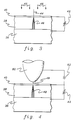
- FIG. 1 depicts a cross-sectional view of proximity effects of electron backscattering in a conventional electron-beam lithographic process.
- FIGs. 2a, 2b depict a top view of residual uncompensated proximity effects due to intended feature shape in a conventional electron-beam lithographic process.
- FIG. 3 depicts a cross-sectional view of an electron-beam lithographic process according to the present invention.
- FIG. 4 depicts the electron-beam lithographic process of FIG. 3 implemented with a high resolution electron exposure instrument according to a second embodiment of the invention.
- FIG. 1 depicts the effects of a conventional E- beam lithography system.
- Substrate 10 is covered with resist layer 12.
- Electron beam 14 is used to create intended feature 16 in the resist.
- Electron beam 14 primary electrons penetrate substrate 10, causing a backscattering 18 of electrons, resulting in a distortion 20 of the intended feature 16. It will be understood that the primary electrons are substantially absorbed in resist layer 12.
- FIG. 2a depicts a top view of neighboring features 22 and 26 desired to be created in resist 24 using E-beam lithography. As the E-beam (not shown) creates feature 22, backscattering electrons penetrate into region 28 of feature 26. This results in undesired curing of feature 26 in region 28, causing a widening of feature 26 in region 28 compared to region 30, as shown in FIG. 2b.
- Every material has a threshold electric field above which the so-called avalanche effect begins.
- the avalanche effect is known, and is basically a large current produced by electrons within a given material when an electric field above the threshold is placed across the material and "catalyst" electrons are introduced into the material. See, for example, G. A. Sai-Halasz and G. Gazecki, Influence of an Electric Field On Beam-induced Adhesion Enhancement, 45 Appl. Phys. Lett. 1067 (1984).
- This threshold depends on the type of material in which avalanche will occur.
- the material of interest is a resist.
- Corona discharge For an example of a prior art Corona discharge E-beam exposure method, see Japanese Patent No. 60-258921 issued to Toshiba, entitled “Method For Exposure by Ion Beam.”
- the present invention for the first time, utilizes the avalanche effect in combination with E- beam lithography to cure the resist using less energy. Since the avalanche effect increases super-linearly with increasing field strength, the resist can easily receive from 100 to 1000 times the exposure that it would have received from the E-beam without the induced field. This means that the E-beam can spend less time over a given area (i.e., throughput is dramatically increased), as well as deliver less charge (i.e., a lower E-beam current).
- FIG. 3 depicts an electron-beam lithographic process according to the present invention.
- a cross- sectional view of a portion of substrate 36 is shown covered by a layer of resist 38 of standard thickness, approximately 0.1 to 2.0 microns.
- the resist layer 38 is coated with a layer of conductive material 40.
- the substrate 36 is a silicon wafer, and the conductive material 40 is a metal, such as aluminum.
- the conductive layer 40 is on the order of 100 angstroms in thickness.
- a bias potential 42 is connected between the conductive layer 40 and the substrate 36.
- Electron path 44 depicts the path of an electron which is part of an electron-beam 45 created in a conventional way. It will be understood that the selected area electron beam 45 cures may comprise a portion of resist layer 38 or the entire layer.
- Avalanche current 46 within the resist layer 38 is created by the combined action of an electron following path 44 and an electric field within resist 38 created by variable bias potential 42.
- the electric field induced in resist 38 is produced by the variable bias potential 42.
- a desired avalanche effect intensity can be achieved through variation in bias potential 42.
- the voltage used to create the field across the resist depends directly on the thickness of the resist. For example, doubling the resist thickness would require a doubling of the voltage to produce the same field strength.
- Conductive layer 40 used here primarily to create the electric field across resist 38, is often used in resist systems as a charge draining layer. Resist is an insulator, and usually relatively thick, so a charge build-up due to the E-beam needs to dissipate, as a charge build-up in the resist may cause E-beam deflection.
- a conductive layer allows the charge to dissipate, and prevents E-beam deflection.
- the addition of conductive layer 14 is not an additional step that must be performed.
- the conductive layer 40 is removed, and the resist goes through the usual development. Often, the conductive layer 40 is removed by dissolving in a standard developer. At the next lithographic level, the process is repeated.
- Electrons involved in the avalanche process are typically of relatively low energy, approximately a few hundred electron volts. With low energy, the electrons cannot migrate very far or cause other electrons to migrate far, thus eliminating short-range proximity effects.
- the direction of the field has not been found to affect this inherent effect. However, it will be understood that certain materials may require, or have more of a pronounced inherent effect with a particular electric field direction. To eliminate any remaining long-range proximity effects or backscattering, variation of the electric field in the resist can be used.
- the process of the present invention can be used to compensate for the distortion depicted in FIG. 2b by lessening the intensity of the electric field (decreasing the variable potential bias) through feature 22, while not decreasing the field strength to or below the threshold. This results in a lessening of the avalanche current effect, and an elimination in the amount of backscattering not eliminated by the addition of the initial electric field across the resist. This also eliminates the FIG. 2b distortion in region 28 of feature 26.
- the varying of the electric field depending on which feature, or which area of a given feature, is being created involves both monitoring and a predetermination of when backscattering overlap may occur. Predetermination of potential backscattering overlap areas is known in the art, and will not be further explained.
- Predetermination of potential backscattering overlap areas is known in the art, and will not be further explained.
- One example is, as shown in FIGs. 2a, 2b, two features created close to one another.
- the first embodiment of the invention provides for the use of the avalanche effect in a resist in the context of E-beam lithography. This greatly enhances throughput over conventional E-beam lithography, eliminates short-range proximity effects, and provides excellent image controllability.
- the first embodiment also provides for the elimination of long-range proximity effects (backscattering) existing in conventional E-beam lithography by providing for a variable electric field strength across the resist to adjust the intensity of avalanche effect in sensitive areas of the feature sought to be produced.
- FIG. 4 depicts a second embodiment of the present invention.
- the E-beam lithography set-up of FIG. 4 is similar to that of FIG. 3, except for the electron delivery system.
- Resist 38 is of standard thickness, approximately 0.1 to 2.0 microns. In general, the resist is typically not much thicker than the feature sought to be created.
- avalanche current 48 induced by incident electrons following path 49, can create even finer features than tne avalanche current 46 of FIG. 3.
- a high resolution electron exposure instrument such as a scanning tunneling microscope (STM), can be sued in conjunction with the avalanche effect to create such ultra-fine features.
- STM scanning tunneling microscope
- the tip 50 of a Scanning Tunneling Microscope (not shown) provides electrons in much fewer numbers than conventional E-beam systems, the STM tip being on the atomic scale, while also providing greater accuracy in their placement. Thus, an STM cannot cure the entire resist layer at once. Rather, an area limited by the electron beam width out of the STM may be exposed.
- STM Scanning Tunneling Microscope
- STM tip 50 is placed in close proximity to conducting layer 40. This distance is small, on the order of 0.001 microns to 0.1 microns.
- a bias potential 52 on the order of 10-100 volts, is created between STM tip 50 and conducting layer 40 to ensure accuracy in electron placement. The higher the voltage, the greater the distance between STM tip 50 and conducting layer 40. STM tip 50 is at a lower potential than conducting layer 40 so the electrons out of the tip are attracted to the conducting layer.
- Electrons supplied by the STM typically have energy on the order of a few electron volts. With such low energy and in such few numbers, the proximity effects seen in conventional E-beam lithography are not of concern.
- the present invention advances the state of the art by providing a high resolution E-beam lithography process with greatly enhanced throughput.
- This allows E-beam lithography, the preferred process for creation of fine features in resist layers, to be used in actual production.
- the present invention also inherently eliminates most of the proximity effects associated with E-beam lithography, and allows for correction of any remaining proximity effects by providing for a variable electric field in the resist layer.
- ultra-fine features can be created through an improved electron delivery system giving much greater control over the placement of fewer electrons.
Landscapes
- Engineering & Computer Science (AREA)
- Chemical & Material Sciences (AREA)
- Nanotechnology (AREA)
- Physics & Mathematics (AREA)
- Crystallography & Structural Chemistry (AREA)
- General Physics & Mathematics (AREA)
- Structural Engineering (AREA)
- Condensed Matter Physics & Semiconductors (AREA)
- Manufacturing & Machinery (AREA)
- Architecture (AREA)
- Analytical Chemistry (AREA)
- Mathematical Physics (AREA)
- Theoretical Computer Science (AREA)
- Electron Beam Exposure (AREA)
Applications Claiming Priority (2)
| Application Number | Priority Date | Filing Date | Title |
|---|---|---|---|
| US95986692A | 1992-10-13 | 1992-10-13 | |
| US959866 | 1992-10-13 |
Publications (1)
| Publication Number | Publication Date |
|---|---|
| EP0593387A2 true EP0593387A2 (de) | 1994-04-20 |
Family
ID=25502511
Family Applications (1)
| Application Number | Title | Priority Date | Filing Date |
|---|---|---|---|
| EP93480136A Withdrawn EP0593387A2 (de) | 1992-10-13 | 1993-09-21 | Elektronenstrahllithographie mit induzierten Strömen |
Country Status (2)
| Country | Link |
|---|---|
| EP (1) | EP0593387A2 (de) |
| JP (1) | JP2592214B2 (de) |
Family Cites Families (1)
| Publication number | Priority date | Publication date | Assignee | Title |
|---|---|---|---|---|
| JP3106650B2 (ja) * | 1992-01-28 | 2000-11-06 | ソニー株式会社 | 電子による反応を利用した微細処理方法 |
-
1993
- 1993-08-23 JP JP5207539A patent/JP2592214B2/ja not_active Expired - Lifetime
- 1993-09-21 EP EP93480136A patent/EP0593387A2/de not_active Withdrawn
Also Published As
| Publication number | Publication date |
|---|---|
| JPH06204128A (ja) | 1994-07-22 |
| JP2592214B2 (ja) | 1997-03-19 |
Similar Documents
| Publication | Publication Date | Title |
|---|---|---|
| Pease | Electron beam lithography | |
| US5831272A (en) | Low energy electron beam lithography | |
| Fischer et al. | 10 nm electron beam lithography and sub‐50 nm overlay using a modified scanning electron microscope | |
| US5395738A (en) | Electron lithography using a photocathode | |
| EP0412690A2 (de) | Herstellung von Vorrichtungen mittels lithographischer Prozesse | |
| JPS596506B2 (ja) | 電子写真製版方法 | |
| US20020036273A1 (en) | Methods for manufacturing reticles for charged-particle-beam microlithography exhibiting reduced proximity effects, and reticles produced using same | |
| Wagner | Applications of focused ion beams | |
| Cerrina et al. | A path to nanolithography | |
| Utsumi | Low energy electron-beam proximity projection lithography: Discovery of a missing link | |
| McCord et al. | Low voltage, high resolution studies of electron beam resist exposure and proximity effect | |
| US4554458A (en) | Electron beam projection lithography | |
| US4329410A (en) | Production of X-ray lithograph masks | |
| US4746587A (en) | Electron emissive mask for an electron beam image projector, its manufacture, and the manufacture of a solid state device using such a mask | |
| JP3251875B2 (ja) | 荷電粒子ビーム露光装置 | |
| US5112724A (en) | Lithographic method | |
| Utsumi | Low-energy e-beam proximity lithography (LEEPL): is the simplest the best? | |
| US20010028037A1 (en) | Hollow-beam aperture for charged-particle-beam optical systems and microlithography apparatus, andbeam-adjustment methods employing same | |
| US4467026A (en) | Process for drawing patterns with extremely fine features in the production of VLSI, LSI and IC systems | |
| EP0593387A2 (de) | Elektronenstrahllithographie mit induzierten Strömen | |
| DE2755399C2 (de) | ||
| US6621090B2 (en) | Electron-beam sources exhibiting reduced spherical aberration, and microlithography apparatus comprising same | |
| EP0200083B1 (de) | Lithographiegerät mittels eines niederenergetischen Elektronenstrahls | |
| Wang et al. | High-resolution x-ray masks for high-aspect-ratio microelectromechanical systems (HARMS) | |
| JPH11329944A (ja) | 荷電ビーム露光装置及び荷電ビーム露光方法 |
Legal Events
| Date | Code | Title | Description |
|---|---|---|---|
| PUAI | Public reference made under article 153(3) epc to a published international application that has entered the european phase |
Free format text: ORIGINAL CODE: 0009012 |
|
| AK | Designated contracting states |
Kind code of ref document: A2 Designated state(s): DE FR GB |
|
| 17P | Request for examination filed |
Effective date: 19940819 |
|
| STAA | Information on the status of an ep patent application or granted ep patent |
Free format text: STATUS: THE APPLICATION HAS BEEN WITHDRAWN |
|
| 18W | Application withdrawn |
Withdrawal date: 19960816 |