EP0590645A1 - Méthode et système pour la réduction de demandes d'allocation de mémoire - Google Patents
Méthode et système pour la réduction de demandes d'allocation de mémoire Download PDFInfo
- Publication number
- EP0590645A1 EP0590645A1 EP93115741A EP93115741A EP0590645A1 EP 0590645 A1 EP0590645 A1 EP 0590645A1 EP 93115741 A EP93115741 A EP 93115741A EP 93115741 A EP93115741 A EP 93115741A EP 0590645 A1 EP0590645 A1 EP 0590645A1
- Authority
- EP
- European Patent Office
- Prior art keywords
- device driver
- buffer
- component device
- collective
- memory
- Prior art date
- Legal status (The legal status is an assumption and is not a legal conclusion. Google has not performed a legal analysis and makes no representation as to the accuracy of the status listed.)
- Granted
Links
- 238000000034 method Methods 0.000 title claims abstract description 39
- 239000000872 buffer Substances 0.000 claims abstract description 177
- 238000010586 diagram Methods 0.000 description 12
- 230000006870 function Effects 0.000 description 12
- 238000004590 computer program Methods 0.000 description 2
- 230000007423 decrease Effects 0.000 description 1
- 230000004048 modification Effects 0.000 description 1
- 238000012986 modification Methods 0.000 description 1
- 230000002093 peripheral effect Effects 0.000 description 1
Images


Classifications
-
- G—PHYSICS
- G06—COMPUTING; CALCULATING OR COUNTING
- G06F—ELECTRIC DIGITAL DATA PROCESSING
- G06F12/00—Accessing, addressing or allocating within memory systems or architectures
- G06F12/02—Addressing or allocation; Relocation
-
- G—PHYSICS
- G06—COMPUTING; CALCULATING OR COUNTING
- G06F—ELECTRIC DIGITAL DATA PROCESSING
- G06F9/00—Arrangements for program control, e.g. control units
- G06F9/06—Arrangements for program control, e.g. control units using stored programs, i.e. using an internal store of processing equipment to receive or retain programs
- G06F9/46—Multiprogramming arrangements
- G06F9/50—Allocation of resources, e.g. of the central processing unit [CPU]
- G06F9/5005—Allocation of resources, e.g. of the central processing unit [CPU] to service a request
- G06F9/5011—Allocation of resources, e.g. of the central processing unit [CPU] to service a request the resources being hardware resources other than CPUs, Servers and Terminals
- G06F9/5016—Allocation of resources, e.g. of the central processing unit [CPU] to service a request the resources being hardware resources other than CPUs, Servers and Terminals the resource being the memory
-
- G—PHYSICS
- G06—COMPUTING; CALCULATING OR COUNTING
- G06F—ELECTRIC DIGITAL DATA PROCESSING
- G06F12/00—Accessing, addressing or allocating within memory systems or architectures
- G06F12/02—Addressing or allocation; Relocation
- G06F12/0223—User address space allocation, e.g. contiguous or non contiguous base addressing
Definitions
- the present invention relates generally to the field of computer architecture, and more particularly to a method and system for reducing memory allocation requests in a layered architecture.
- a computer system may execute a number of software routines. These software routines may require the dynamic memory allocation and deallocation of a particular amount of available computer memory to use as work space.
- dynamic memory allocation memory is allocated as needed during execution of software routines.
- a software routine starts execution, it requests the dynamic allocation of computer memory.
- the software routine completes execution, it deallocates the allocated computer memory.
- the deallocated computer memory is then available for reallocation.
- such an allocation and deallocation occurs every time a software routine is invoked.
- a large number of software routines must be invoked, a corresponding large number of computer memory allocations and deallocations are required.
- An object of the present invention is to provide a computer method and system for dynamically allocating a collective buffer of computer memory to a plurality of software routines.
- Another object of the present invention is to provide a computer method and system for maintaining, for each software routine, an offset that indicates the location of work space within the collective buffer provided for that software routine.
- Another object of the present invention is to provide a computer method and system for allocating a collective device driver buffer to a plurality of component device drivers prior to execution of any of the component device drivers and accessing corresponding portions of the collective device driver buffer as work space for each component device driver invoked to process an input/output (I/O) operation.
- I/O input/output
- a computer method and system for allocating memory for a plurality of software routines is allocated.
- Each software routine is assigned an offset within the collective buffer.
- Each software routine may then use the portion of the collective buffer starting at its offset as its dynamically allocated work space.
- a collective buffer size is first determined which is sufficient to satisfy the total dynamic memory requirements of the software routines. In determining the collective buffer size, the size of a software routine buffer required by each software routine is accumulated into the collective buffer size. As each software routine buffer size requirement is accumulated, the total is stored as the offset for the next software routine.
- the total indicates the collective buffer size.
- the collective buffer of the collective buffer size is then allocated.
- each software routine uses a portion of the collective buffer referenced by its assigned offset.
- the collective buffer may then be deallocated.
- the memory is allocated to a software system having a layered architecture including an application program and a device driver comprising a plurality of component device drivers.
- Each component device driver when executed performs functions necessary to process an I/O request from the application program.
- a device driver buffer is allocated having a size based on a total of the work space requirements of all of the component device drivers.
- a call-down table is accessed which contains a call-down table entry for each component device driver.
- the call-down table entry contains a pointer to the corresponding component device driver and an offset within the device driver buffer.
- Each component device driver processes the I/O request using a portion of the device driver buffer beginning at this offset as its work space.
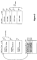
- Figure 1 is a block diagram showing a computer with a software system having a layered architecture.
- Figure 2 is a block diagram illustrating sample data structures of the present invention.
- Figure 3 is a flow diagram of a routine for determining the buffer sizes and buffer offsets of component device drivers.
- Figure 4 is a flow diagram of a routine for allocating memory to perform an I/O operation.
- Figure 5 is a flow diagram of a routine for processing an I/O request.
- Figure 6 is a flow diagram representing the processing performed by a device driver.
- FIG. 1 is a block diagram showing a computer with a software system having a layered architecture.
- the computer 101 includes I/O devices, memory, and a processor (not shown). Within the memory is stored a layered architecture system 102 which is executed by the processor.
- the layered architecture system comprises an application program 103, a file system driver 104, I/O supervisor (IOS) 105, and device driver 109.
- Device driver 109 comprises component device drivers 106, 107, and 108.
- the component device drivers 106, 107, and 108 each perform a specific function related to accessing a corresponding device.
- the component drivers are configured into the device driver during startup of the computer system.
- the layered architecture system is shown in Figure 1 as its components 103-108 are conceptually related as layers.
- Computer programs in the higher layers request services of the computer programs in the lower layers.
- application program 103 requests services of the file system driver 104 by sending it file system requests, such as file read or write requests.
- the file system driver 104 receives these file system requests and performs functions such as converting a file read request (to read a particular location in a file) to a request to read a corresponding location relative to the actual disk address at which the file is stored.
- the file system driver then passes on the request to read data to the I/O supervisor 105.
- the I/O supervisor passes on the read request to the device driver 109 by invoking component device driver 106.
- Each component device driver when executed performs a particular function relating to retrieving data from the disk.
- component device driver 106 may implement disk caching
- component device driver 107 may encrypt/decrypt data
- component device driver 108 may directly access the disk for reading and writing data.
- the device driver 106 retrieves the data from its cache buffer to satisfy this request. If, however, the data is not stored within the cache buffer, then the request cannot be satisfied by the component device driver 106, and component device driver 106 passes on the request to component device driver 107.
- Component device driver 107 may, for example, encrypt and decrypt data transferred to and from the disk. Because the file system request is a ead request, component device driver 107 cannot satisfy the request, but passes on the request to component device driver 108. Component device driver 108 actually retrieves the data from the disk and returns the data to component device driver 107. Component device driver 107 then decrypts the data and passes the data to component device driver 106. Component device driver 106 passes the data to the I/O supervisor 105 after storing the data in its cache buffers. The I/O supervisor 105 passes the data to the file system driver 104, and finally the file system driver 104 passes the data to the application program 103.
- each of the layers can be developed and tested independently of one another.
- One software developer could develop component device driver 106, which performs the disk caching.
- Another software developer could develop component device driver 107 to encrypt and decrypt data. So long as the interfaces between the layers are well defined, the various component device drivers can be configured properly into a layered architecture as described above.
- Such a layered architecture is described in U.S. Patent Application 07/954,920 entitled “Method and System for Configuring and Executing Device Drivers,” which is hereby incorporated by reference.
- a disadvantage of a layered architecture occurs, however, when each layer is required to be separately allocated the work space memory necessary to perform its function. For example, when component device driver 106 is invoked to perform disk caching, it would request the operating system to provide a memory allocation of work space for it to perform the disk caching. Before returning, the component device driver 106 would request deallocation of its work space memory. Similarly, component device drivers 107 and 108 would also request allocations and deallocations of work space memory. This allocation and deallocation of work spaces for each component driver may result in unacceptable burden on the computer system.
- the present invention reduces this burden by allocating, prior to executing software routines (e.g. component device drivers), an amount of memory necessary to satisfy the requirements of all the software routines.
- a collective buffer is created having a collective buffer size sufficient to satisfy a total of all of these memory requirements. Offsets are stored for each software routine, calculated from the individual memory requirements of that software routine, for locating a corresponding software routine buffer within the collective buffer which contains the work space for that software routine.
- the operating system allocates, prior to invocation of the component device drivers, memory sufficient to satisfy the memory requirements of all component device drivers.
- the memory requirement of each such component device driver is determined and accumulated to calculate the size of a device driver buffer necessary to contain the work space for all component device drivers. These memory requirements are also used to determine offsets which are used by each component device driver to reference its own work space within the collective buffer.
- FIG. 2 is a block diagram illustrating sample data structures of the present invention.
- the I/O supervisor maintains in memory a device control block 210 for each peripheral device.
- the device control block 210 contains the address of a call-down table (CDT) 201.
- the call-down table contains a CDT entry 202, 203, 204 for each component device driver of the device driver. Each CDT entry contains the address of the component device driver.
- the device control block accessed to determine the size of buffers needed by the device driver during execution, and to locate the call-down table.
- the call-down table has the location of each component device driver within the device driver and the location of each component device driver buffer having work space for the corresponding component device driver.
- the call-down table is accessed to invoke each component device driver therein.
- Each component device driver performs a function of the device driver in accessing the corresponding device, using the corresponding component device driver buffer as work space. Because execution of a device driver occurs after the component device drivers have been configured into layers within the device driver, the call-down table represents the component device drivers to be called during execution of the device driver.
- the file system driver identifies an input/output packet (IOP) buffer 220 when passing a request to the input/output supervisor (IOS) to retrieve or store data.
- the IOP buffer 220 contains an IOS buffer 221, an input/output request (IOR) buffer 222, and component device driver (CDD) buffers 223, 224, and 225.
- the IOS uses the IOS buffer 221 to store its internal state information.
- the IOS stores a description of the I/O request received from an application into the IOR buffer 222.
- Each component device driver accesses the IOR buffer to determine the request.
- the IOR buffer size is determined by the IOS.
- Each of these component device driver buffers is used to provide work space to the corresponding component device driver.
- the component device driver buffers are collectively referred to as the device driver (DD) buffer 226.
- Figure 3 is a flow diagram of a routine for determining the buffer size requirements and buffer offsets of the component device drivers.
- This routine called IOS_determine_CDD_buffersizes, is invoked by the IOS upon execution of a device driver to access a corresponding device.
- the routine determines the buffer size requirements and inserts in the call-down table an offset from the beginning of the device driver buffer 226.
- the offset indicates the start of the component device driver buffer work space for the corresponding component device driver.
- the routine sets a variable, called offset, equal to zero.
- the variable offset is used to track the offset of a component device driver buffer from the beginning of the device driver buffer 226.
- the routine performs a loop, determining the size of each component device driver buffer and updating the call-down table accordingly.
- the routine selects the next component device driver by referencing the component device driver in the call-down table via the device control block, starting with the "bottom most" component device driver.
- the bottom most component device driver is, in the example of Figure 1, component device driver 108.
- the routine stores the variable offset in the CDT entry for the selected component device driver.
- the routine determines the buffer size of the selected component device driver.
- the buffer size requirement of the selected component device driver may be determined by requesting the buffer size requirement from the selected component device driver each time this routine is invoked. Thus, each component device driver can dynamically determine its memory needs. Alternatively, the buffer size requirement could be determined once at system startup.
- step 305 the routine increases the variable offset by the determined buffer size requirement of the selected component device driver.
- step 306 if all component device drivers have already been selected, the routine continues at step 307. Otherwise, the routine loops to step 302 to select the next component device driver.
- step 307 the routine sets the total size of the device driver buffer to equal the variable offset, e.g. the bottom of the buffer, and the routine returns.
- the offset denotes the location of each next component device driver's buffer in the IOP buffer and, upon exiting the loop, the total size of the device driver buffer.
- Figures 4-6 illustrate the processing of an I/O request by a device driver using the collective buffer to provide work space for each component device driver within the device driver.
- Figure 4 shows the FSD_Request routine performed by the File System Driver upon receiving a request to perform and I/O operation. This routine determines the size of the buffers necessary for the appropriate Device Driver to process the request, allocates memory for these buffers, calls the IOS_Request routine shown in Figure 5 to process the request, and then deallocates the memory.
- the IOS_Request routine in Figure 5 selects the first component device driver in the device driver, calling the component device driver routine shown in Figure 6 to invoke the component device driver.
- Figure 6 shows the process performed by an invoked component device driver, which includes processing the I/O request by performing a component device driver-specific function such as encryption, etc., and invoking, where appropriate, a next component device driver to perform another component device driver-specific function.
- Each component device driver calculates an address of a corresponding component device driver buffer based on a corresponding offset and uses the corresponding component device driver buffer as work space while performing its component device driver-specific function.
- FIG. 4 is a flow diagram of a routine for allocating memory to perform an I/O operation.
- This routine called FSD_Request, is part of the file system driver (FSD) and is invoked upon a request by an application program to perform an I/O operation.
- the routine receives file system requests from an application program and processes the requests.
- the routine allocates an IOP buffer, initializes the IOR buffer data, invokes the IOS passing it a pointer to the IOP buffer, and deallocates the IOP buffer.
- the routine determines the size of the device driver buffer, the IOS buffer, and the IOR buffer. In a preferred embodiment, the FSD determines these sizes by requesting the data from the IOS.
- the IOS determines the buffer size, which varies based on the number and type of component device drivers. This is preferably done by the IOS by invoking the IOS_determine_CDD_buffersizes routine.
- the routine determines the size of the IOP buffer.
- the size of the IOP buffer is the total size of the device driver buffer plus the size of the IOS buffer plus the size of the IOR buffer.
- the routine allocates an IOP buffer of the determined IOP buffer size. This allocation is essentially the identification of memory space adequate to accommodate the buffer requirements.
- step 404 the routine initializes the IOR buffer. This initialization stores in the IOR buffer information describing the I/O request, which may involve, for example, the translation of a logical file system address to a physical disk address.
- step 405 the routine invokes the routine IOS_Request, passing it the IOP buffer.
- step 406 the routine deallocates the IOP buffer. The routine then returns.
- FIG. 5 is a flow diagram of a routine for processing an I/O request.
- the routine called IOS_Request, is invoked by the FSD_Request routine.
- This routine invokes the component device driver identified in the first CDT entry, passing a pointer to the IOP buffer.
- the routine stores in the IOS buffer the address of the first CDT entry in the call-down table.
- the routine invokes the component device driver of the selected CDT entry, passing the IOP buffer, the size of the IOS buffer, and the size of the IOR buffer. The routine then returns.
- Figure 6 is a flow diagram representing the processing performed by a component device driver routine.
- the "top most" component device driver routine is invoked by the FSD_Request routine to process an I/O request to access a corresponding device.
- the topmost component device driver then invokes the next lower component device driver, which invokes the next lower component device driver.
- the routine selects the CDT entry whose address is in the IOS buffer. This address corresponds to the entry for the component device driver itself, and denotes the address of a first component device driver in the device driver.
- the routine retrieves from the selected CDT entry the offset of the component device driver buffer.
- the routine determines the address of the buffer for this component device driver by adding the offset to a base address.
- the base address is the address of the IOP buffer plus the size of the IOS buffer plus the size of the IOR buffer.
- the routine processes the I/O request by performing a component device driver-specific function. This function may involve, for example, retrieving data from the disk cache buffer or encrypting data.
- step 605 if the selected CDT entry is the last entry in the CDT, then the routine continues at step 609. Otherwise, the routine continues at step 606.
- step 606 the routine selects the next CDT entry.
- step 607 the routine stores the address of the selected CDT entry in the IOS buffer.
- step 608 the routine invokes the component device driver of the selected CDT entry, passing it a pointer to the IOP buffer, the size of the IOS buffer, and the size of the IOR buffer.
- Each component device driver performs as described in Figure 6, except that for each component device driver, a different component device driver-specific function is performed.
- step 609 the routine performs component device driver-specific processing of the I/O request for the final component device driver in the device driver. This processing may involve, for example, storing data in the disk cache buffer or decrypting data. The routine then returns.
Landscapes
- Engineering & Computer Science (AREA)
- Theoretical Computer Science (AREA)
- Physics & Mathematics (AREA)
- General Engineering & Computer Science (AREA)
- General Physics & Mathematics (AREA)
- Software Systems (AREA)
- Stored Programmes (AREA)
- Memory System (AREA)
- Memory System Of A Hierarchy Structure (AREA)
- Hardware Redundancy (AREA)
- Storage Device Security (AREA)
- Saccharide Compounds (AREA)
Applications Claiming Priority (2)
| Application Number | Priority Date | Filing Date | Title |
|---|---|---|---|
| US95447492A | 1992-09-30 | 1992-09-30 | |
| US954474 | 1992-09-30 |
Publications (2)
| Publication Number | Publication Date |
|---|---|
| EP0590645A1 true EP0590645A1 (fr) | 1994-04-06 |
| EP0590645B1 EP0590645B1 (fr) | 2000-07-19 |
Family
ID=25495470
Family Applications (1)
| Application Number | Title | Priority Date | Filing Date |
|---|---|---|---|
| EP93115741A Expired - Lifetime EP0590645B1 (fr) | 1992-09-30 | 1993-09-29 | Méthode et système pour la réduction de demandes d'allocation de mémoire |
Country Status (11)
| Country | Link |
|---|---|
| US (1) | US5675793A (fr) |
| EP (1) | EP0590645B1 (fr) |
| JP (1) | JP3421092B2 (fr) |
| KR (1) | KR940007680A (fr) |
| AT (1) | ATE194874T1 (fr) |
| CA (1) | CA2107387C (fr) |
| DE (1) | DE69329047T2 (fr) |
| DK (1) | DK0590645T3 (fr) |
| ES (1) | ES2149795T3 (fr) |
| GR (1) | GR3034591T3 (fr) |
| PT (1) | PT590645E (fr) |
Cited By (5)
| Publication number | Priority date | Publication date | Assignee | Title |
|---|---|---|---|---|
| US5787019A (en) * | 1996-05-10 | 1998-07-28 | Apple Computer, Inc. | System and method for handling dynamic changes in device states |
| US5835737A (en) * | 1996-05-10 | 1998-11-10 | Apple Computer, Inc. | Method and apparatus for arbitrating access to selected computer system devices |
| GB2342470A (en) * | 1998-10-09 | 2000-04-12 | Ibm | A memory management system and method for a data processing system |
| EP1244221A1 (fr) * | 2001-03-23 | 2002-09-25 | Sun Microsystems, Inc. | Procédé et système pour éliminer des données rédondantes |
| US20220188785A1 (en) * | 2020-12-14 | 2022-06-16 | Secure, Inc. | Administering and automating a sponsored emergency savings program |
Families Citing this family (29)
| Publication number | Priority date | Publication date | Assignee | Title |
|---|---|---|---|---|
| WO1997028501A1 (fr) * | 1996-01-31 | 1997-08-07 | International Business Machines Corporation | Systeme et procede de surveillance |
| US5758154A (en) * | 1996-06-05 | 1998-05-26 | Microsoft Corporation | Method and system for storing configuration data into a common registry |
| US6209041B1 (en) | 1997-04-04 | 2001-03-27 | Microsoft Corporation | Method and computer program product for reducing inter-buffer data transfers between separate processing components |
| US5916309A (en) * | 1997-05-12 | 1999-06-29 | Lexmark International Inc. | System for dynamically determining the size and number of communication buffers based on communication parameters at the beginning of the reception of message |
| US5926227A (en) * | 1997-07-28 | 1999-07-20 | Lsi Logic Corporation | Video decoder dynamic memory allocation system and method with error recovery |
| US6023712A (en) * | 1997-07-30 | 2000-02-08 | Quarterdeck Corporation | Method and apparatus for brokering memory resources |
| KR100450957B1 (ko) * | 1997-12-30 | 2004-12-14 | 삼성전자주식회사 | 메인 통신 보드 상에서 서브 통신 보드 데이터를 일정하게읽기 위한 방법 |
| US6154822A (en) * | 1998-04-21 | 2000-11-28 | International Business Machines Corporation | Method and system for improving data storage and access for programs written in mid-level programming languages |
| US6463537B1 (en) * | 1999-01-04 | 2002-10-08 | Codex Technologies, Inc. | Modified computer motherboard security and identification system |
| US7000106B2 (en) * | 1999-03-26 | 2006-02-14 | Siemens Communications, Inc. | Methods and apparatus for kernel mode encryption of computer telephony |
| US6600493B1 (en) | 1999-12-29 | 2003-07-29 | Intel Corporation | Allocating memory based on memory device organization |
| US6724390B1 (en) * | 1999-12-29 | 2004-04-20 | Intel Corporation | Allocating memory |
| US7035916B1 (en) * | 2000-02-16 | 2006-04-25 | Microsoft Corporation | Coupling a filter graph space to a network driver space |
| WO2003009144A1 (fr) * | 2001-07-19 | 2003-01-30 | Wind River Systems, Inc. | Systeme de gestion memoire |
| US7055152B1 (en) * | 2001-08-15 | 2006-05-30 | Microsoft Corporation | Method and system for maintaining buffer registrations in a system area network |
| US7594265B2 (en) * | 2001-11-14 | 2009-09-22 | Ati Technologies, Inc. | System for preventing unauthorized access to sensitive data and a method thereof |
| US7024672B2 (en) * | 2002-06-26 | 2006-04-04 | Microsoft Corporation | Process-mode independent driver model |
| US7080172B1 (en) | 2003-05-27 | 2006-07-18 | Marvell Luternational Ltd. | Management of memory, hardware and associated device drivers using stacks |
| US7844758B1 (en) | 2003-06-18 | 2010-11-30 | Advanced Micro Devices, Inc. | Dynamic resource allocation scheme for efficient use of a queue |
| US7418716B2 (en) * | 2003-12-19 | 2008-08-26 | Intel Corporation | Method, apparatus, system, and article of manufacture for interfacing a device |
| US7421700B2 (en) * | 2004-03-15 | 2008-09-02 | Microsoft Corporation | Interprocess buffer management using a buffer delay time |
| CN100392621C (zh) * | 2005-10-14 | 2008-06-04 | 威盛电子股份有限公司 | 总线控制器及数据缓冲空间分配方法 |
| US20070214347A1 (en) * | 2006-03-13 | 2007-09-13 | Rothman Michael A | Method and apparatus for performing staged memory initialization |
| US7908412B2 (en) * | 2006-05-10 | 2011-03-15 | Microsoft Corporation | Buffer passing mechanisms |
| CN101996082B (zh) | 2009-08-28 | 2014-06-11 | 国际商业机器公司 | 协处理器系统和在本地存储器上加载应用程序的方法 |
| WO2011121168A1 (fr) * | 2010-03-31 | 2011-10-06 | Nokia Corporation | Système et procédé d'attribution de tampons |
| US9244828B2 (en) * | 2012-02-15 | 2016-01-26 | Advanced Micro Devices, Inc. | Allocating memory and using the allocated memory in a workgroup in a dispatched data parallel kernel |
| CN109213596B (zh) * | 2018-08-01 | 2023-03-10 | 青岛海信移动通信技术股份有限公司 | 一种分配终端内存的方法和设备 |
| CN111208933B (zh) * | 2018-11-21 | 2023-06-30 | 昆仑芯(北京)科技有限公司 | 数据访问的方法、装置、设备和存储介质 |
Citations (1)
| Publication number | Priority date | Publication date | Assignee | Title |
|---|---|---|---|---|
| EP0456275A2 (fr) * | 1990-05-11 | 1991-11-13 | Fujitsu Limited | SystÀ¨me d'allocation de mémoire statique |
Family Cites Families (1)
| Publication number | Priority date | Publication date | Assignee | Title |
|---|---|---|---|---|
| US5367637A (en) * | 1992-03-26 | 1994-11-22 | International Business Machines Corporation | Self-tuning virtual storage management for dedicated real-time computer system |
-
1993
- 1993-09-28 KR KR1019930020110A patent/KR940007680A/ko not_active Application Discontinuation
- 1993-09-29 ES ES93115741T patent/ES2149795T3/es not_active Expired - Lifetime
- 1993-09-29 PT PT93115741T patent/PT590645E/pt unknown
- 1993-09-29 AT AT93115741T patent/ATE194874T1/de active
- 1993-09-29 DK DK93115741T patent/DK0590645T3/da active
- 1993-09-29 EP EP93115741A patent/EP0590645B1/fr not_active Expired - Lifetime
- 1993-09-29 JP JP24303893A patent/JP3421092B2/ja not_active Expired - Lifetime
- 1993-09-29 DE DE69329047T patent/DE69329047T2/de not_active Expired - Fee Related
- 1993-09-29 CA CA002107387A patent/CA2107387C/fr not_active Expired - Fee Related
-
1996
- 1996-01-03 US US08/582,219 patent/US5675793A/en not_active Expired - Lifetime
-
2000
- 2000-10-11 GR GR20000402280T patent/GR3034591T3/el not_active IP Right Cessation
Patent Citations (1)
| Publication number | Priority date | Publication date | Assignee | Title |
|---|---|---|---|---|
| EP0456275A2 (fr) * | 1990-05-11 | 1991-11-13 | Fujitsu Limited | SystÀ¨me d'allocation de mémoire statique |
Non-Patent Citations (2)
| Title |
|---|
| "Termination of a pool of memory selectors with a single API call", IBM TECHNICAL DISCLOSURE BULLETIN, vol. 35, no. 1A, June 1992 (1992-06-01), NEW YORK US, pages 384 - 385 * |
| HANSON: "Fast allocation and deallocation of memory based on object lifetimes", SOFTWARE PRACTICE & EXPERIENCE, vol. 20, no. 1, January 1990 (1990-01-01), CHICHESTER GB, pages 5 - 12, XP000095792, DOI: doi:10.1002/spe.4380200104 * |
Cited By (8)
| Publication number | Priority date | Publication date | Assignee | Title |
|---|---|---|---|---|
| US5787019A (en) * | 1996-05-10 | 1998-07-28 | Apple Computer, Inc. | System and method for handling dynamic changes in device states |
| US5835737A (en) * | 1996-05-10 | 1998-11-10 | Apple Computer, Inc. | Method and apparatus for arbitrating access to selected computer system devices |
| GB2342470A (en) * | 1998-10-09 | 2000-04-12 | Ibm | A memory management system and method for a data processing system |
| EP1244221A1 (fr) * | 2001-03-23 | 2002-09-25 | Sun Microsystems, Inc. | Procédé et système pour éliminer des données rédondantes |
| US6889297B2 (en) | 2001-03-23 | 2005-05-03 | Sun Microsystems, Inc. | Methods and systems for eliminating data redundancies |
| US20220188785A1 (en) * | 2020-12-14 | 2022-06-16 | Secure, Inc. | Administering and automating a sponsored emergency savings program |
| US11748720B2 (en) * | 2020-12-14 | 2023-09-05 | Secure, Inc. | Administering and automating a sponsored emergency savings program |
| US20240062174A1 (en) * | 2020-12-14 | 2024-02-22 | Secure, Inc. | Administering and automating a sponsored emergency savings program |
Also Published As
| Publication number | Publication date |
|---|---|
| CA2107387C (fr) | 2001-02-27 |
| ES2149795T3 (es) | 2000-11-16 |
| DK0590645T3 (da) | 2000-12-04 |
| JPH06318173A (ja) | 1994-11-15 |
| JP3421092B2 (ja) | 2003-06-30 |
| DE69329047T2 (de) | 2000-12-21 |
| EP0590645B1 (fr) | 2000-07-19 |
| DE69329047D1 (de) | 2000-08-24 |
| CA2107387A1 (fr) | 1994-03-31 |
| US5675793A (en) | 1997-10-07 |
| GR3034591T3 (en) | 2001-01-31 |
| KR940007680A (ko) | 1994-04-27 |
| PT590645E (pt) | 2000-12-29 |
| ATE194874T1 (de) | 2000-08-15 |
Similar Documents
| Publication | Publication Date | Title |
|---|---|---|
| US5675793A (en) | Dynamic allocation of a common buffer for use by a set of software routines | |
| US5802341A (en) | Method for the dynamic allocation of page sizes in virtual memory | |
| US6460126B1 (en) | Computer resource management system | |
| US4761737A (en) | Method to automatically increase the segment size of unix files in a page segmented virtual memory data processing system | |
| US5539899A (en) | System and method for handling a segmented program in a memory for a multitasking data processing system utilizing paged virtual storage | |
| EP0814405B1 (fr) | Procédé et appareil pour le traitement d'information et système d'attribution de mémoire | |
| EP0238158B1 (fr) | Utilisation partagée de segments du type "copie à l'écriture" dans un système de traitement de données à machines virtuelles possédant une mémoire virtuelle | |
| US4511964A (en) | Dynamic physical memory mapping and management of independent programming environments | |
| US4742447A (en) | Method to control I/O accesses in a multi-tasking virtual memory virtual machine type data processing system | |
| US5930827A (en) | Method and apparatus for dynamic memory management by association of free memory blocks using a binary tree organized in an address and size dependent manner | |
| US6125430A (en) | Virtual memory allocation in a virtual address space having an inaccessible gap | |
| EP0676691A2 (fr) | Dispositif pour la sauvegarde et la restauration de registres dans un calculateur numérique | |
| JP4599172B2 (ja) | フリーバッファプールを使用することによるメモリの管理 | |
| US20080162863A1 (en) | Bucket based memory allocation | |
| US11880298B2 (en) | Allocation of memory within a data type-specific memory heap | |
| US5940868A (en) | Large memory allocation method and apparatus | |
| JPH04213129A (ja) | メモリ管理システム及びメモリ管理方法 | |
| EP0403124A2 (fr) | Echange de segments de recouvrement | |
| US8151086B2 (en) | Early detection of an access to de-allocated memory | |
| EP1971922B1 (fr) | Architecture de memoire et procede d'acces | |
| US6600493B1 (en) | Allocating memory based on memory device organization | |
| US7240176B2 (en) | Apparatus and methods for placing a managed heap | |
| US6499094B1 (en) | Management of memory heap space for data files accessible to programs operating in different addressing modes | |
| JP2535584B2 (ja) | 実記憶固定処理計算機 | |
| JPH08507630A (ja) | メモリ管理装置およびメモリ管理方法 |
Legal Events
| Date | Code | Title | Description |
|---|---|---|---|
| PUAI | Public reference made under article 153(3) epc to a published international application that has entered the european phase |
Free format text: ORIGINAL CODE: 0009012 |
|
| AK | Designated contracting states |
Kind code of ref document: A1 Designated state(s): AT BE CH DE DK ES FR GB GR IE IT LI LU MC NL PT SE |
|
| 17P | Request for examination filed |
Effective date: 19940920 |
|
| 17Q | First examination report despatched |
Effective date: 19990115 |
|
| GRAG | Despatch of communication of intention to grant |
Free format text: ORIGINAL CODE: EPIDOS AGRA |
|
| GRAG | Despatch of communication of intention to grant |
Free format text: ORIGINAL CODE: EPIDOS AGRA |
|
| GRAH | Despatch of communication of intention to grant a patent |
Free format text: ORIGINAL CODE: EPIDOS IGRA |
|
| GRAH | Despatch of communication of intention to grant a patent |
Free format text: ORIGINAL CODE: EPIDOS IGRA |
|
| GRAA | (expected) grant |
Free format text: ORIGINAL CODE: 0009210 |
|
| AK | Designated contracting states |
Kind code of ref document: B1 Designated state(s): AT BE CH DE DK ES FR GB GR IE IT LI LU MC NL PT SE |
|
| REF | Corresponds to: |
Ref document number: 194874 Country of ref document: AT Date of ref document: 20000815 Kind code of ref document: T |
|
| REG | Reference to a national code |
Ref country code: CH Ref legal event code: NV Representative=s name: BOVARD AG PATENTANWAELTE Ref country code: CH Ref legal event code: EP |
|
| REG | Reference to a national code |
Ref country code: IE Ref legal event code: FG4D |
|
| ET | Fr: translation filed | ||
| REF | Corresponds to: |
Ref document number: 69329047 Country of ref document: DE Date of ref document: 20000824 |
|
| PGFP | Annual fee paid to national office [announced via postgrant information from national office to epo] |
Ref country code: CH Payment date: 20000904 Year of fee payment: 8 |
|
| PGFP | Annual fee paid to national office [announced via postgrant information from national office to epo] |
Ref country code: SE Payment date: 20000905 Year of fee payment: 8 Ref country code: MC Payment date: 20000905 Year of fee payment: 8 Ref country code: DK Payment date: 20000905 Year of fee payment: 8 |
|
| PGFP | Annual fee paid to national office [announced via postgrant information from national office to epo] |
Ref country code: AT Payment date: 20000906 Year of fee payment: 8 |
|
| PGFP | Annual fee paid to national office [announced via postgrant information from national office to epo] |
Ref country code: LU Payment date: 20000915 Year of fee payment: 8 |
|
| PGFP | Annual fee paid to national office [announced via postgrant information from national office to epo] |
Ref country code: NL Payment date: 20000920 Year of fee payment: 8 |
|
| PGFP | Annual fee paid to national office [announced via postgrant information from national office to epo] |
Ref country code: GR Payment date: 20000928 Year of fee payment: 8 |
|
| PGFP | Annual fee paid to national office [announced via postgrant information from national office to epo] |
Ref country code: PT Payment date: 20000929 Year of fee payment: 8 Ref country code: IE Payment date: 20000929 Year of fee payment: 8 |
|
| ITF | It: translation for a ep patent filed | ||
| PGFP | Annual fee paid to national office [announced via postgrant information from national office to epo] |
Ref country code: BE Payment date: 20001004 Year of fee payment: 8 |
|
| PGFP | Annual fee paid to national office [announced via postgrant information from national office to epo] |
Ref country code: ES Payment date: 20001006 Year of fee payment: 8 |
|
| REG | Reference to a national code |
Ref country code: ES Ref legal event code: FG2A Ref document number: 2149795 Country of ref document: ES Kind code of ref document: T3 |
|
| REG | Reference to a national code |
Ref country code: DK Ref legal event code: T3 |
|
| REG | Reference to a national code |
Ref country code: PT Ref legal event code: SC4A Free format text: AVAILABILITY OF NATIONAL TRANSLATION Effective date: 20000918 |
|
| PLBE | No opposition filed within time limit |
Free format text: ORIGINAL CODE: 0009261 |
|
| STAA | Information on the status of an ep patent application or granted ep patent |
Free format text: STATUS: NO OPPOSITION FILED WITHIN TIME LIMIT |
|
| 26N | No opposition filed | ||
| PGFP | Annual fee paid to national office [announced via postgrant information from national office to epo] |
Ref country code: FR Payment date: 20010831 Year of fee payment: 9 Ref country code: DE Payment date: 20010831 Year of fee payment: 9 |
|
| PGFP | Annual fee paid to national office [announced via postgrant information from national office to epo] |
Ref country code: GB Payment date: 20010904 Year of fee payment: 9 |
|
| PG25 | Lapsed in a contracting state [announced via postgrant information from national office to epo] |
Ref country code: MC Free format text: LAPSE BECAUSE OF NON-PAYMENT OF DUE FEES Effective date: 20010929 Ref country code: LU Free format text: LAPSE BECAUSE OF NON-PAYMENT OF DUE FEES Effective date: 20010929 Ref country code: DK Free format text: LAPSE BECAUSE OF NON-PAYMENT OF DUE FEES Effective date: 20010929 Ref country code: AT Free format text: LAPSE BECAUSE OF NON-PAYMENT OF DUE FEES Effective date: 20010929 |
|
| PG25 | Lapsed in a contracting state [announced via postgrant information from national office to epo] |
Ref country code: SE Free format text: LAPSE BECAUSE OF NON-PAYMENT OF DUE FEES Effective date: 20010930 Ref country code: LI Free format text: LAPSE BECAUSE OF NON-PAYMENT OF DUE FEES Effective date: 20010930 Ref country code: GR Free format text: LAPSE BECAUSE OF NON-PAYMENT OF DUE FEES Effective date: 20010930 Ref country code: ES Free format text: LAPSE BECAUSE OF NON-PAYMENT OF DUE FEES Effective date: 20010930 Ref country code: CH Free format text: LAPSE BECAUSE OF NON-PAYMENT OF DUE FEES Effective date: 20010930 Ref country code: BE Free format text: LAPSE BECAUSE OF NON-PAYMENT OF DUE FEES Effective date: 20010930 |
|
| PG25 | Lapsed in a contracting state [announced via postgrant information from national office to epo] |
Ref country code: IE Free format text: LAPSE BECAUSE OF FAILURE TO SUBMIT A TRANSLATION OF THE DESCRIPTION OR TO PAY THE FEE WITHIN THE PRESCRIBED TIME-LIMIT Effective date: 20011001 |
|
| REG | Reference to a national code |
Ref country code: GB Ref legal event code: IF02 |
|
| BERE | Be: lapsed |
Owner name: MICROSOFT CORP. Effective date: 20010930 |
|
| PG25 | Lapsed in a contracting state [announced via postgrant information from national office to epo] |
Ref country code: PT Free format text: LAPSE BECAUSE OF NON-PAYMENT OF DUE FEES Effective date: 20020331 |
|
| PG25 | Lapsed in a contracting state [announced via postgrant information from national office to epo] |
Ref country code: NL Free format text: LAPSE BECAUSE OF NON-PAYMENT OF DUE FEES Effective date: 20020401 |
|
| EUG | Se: european patent has lapsed |
Ref document number: 93115741.6 |
|
| REG | Reference to a national code |
Ref country code: CH Ref legal event code: PL |
|
| NLV4 | Nl: lapsed or anulled due to non-payment of the annual fee |
Effective date: 20020401 |
|
| REG | Reference to a national code |
Ref country code: DK Ref legal event code: EBP |
|
| REG | Reference to a national code |
Ref country code: PT Ref legal event code: MM4A Free format text: LAPSE DUE TO NON-PAYMENT OF FEES Effective date: 20020331 |
|
| REG | Reference to a national code |
Ref country code: IE Ref legal event code: MM4A |
|
| PG25 | Lapsed in a contracting state [announced via postgrant information from national office to epo] |
Ref country code: GB Free format text: LAPSE BECAUSE OF NON-PAYMENT OF DUE FEES Effective date: 20020929 |
|
| PG25 | Lapsed in a contracting state [announced via postgrant information from national office to epo] |
Ref country code: DE Free format text: LAPSE BECAUSE OF NON-PAYMENT OF DUE FEES Effective date: 20030401 |
|
| GBPC | Gb: european patent ceased through non-payment of renewal fee |
Effective date: 20020929 |
|
| NLV4 | Nl: lapsed or anulled due to non-payment of the annual fee |
Effective date: 20020401 |
|
| PG25 | Lapsed in a contracting state [announced via postgrant information from national office to epo] |
Ref country code: FR Free format text: LAPSE BECAUSE OF NON-PAYMENT OF DUE FEES Effective date: 20030603 |
|
| REG | Reference to a national code |
Ref country code: FR Ref legal event code: ST |
|
| REG | Reference to a national code |
Ref country code: ES Ref legal event code: FD2A Effective date: 20021011 |
|
| PG25 | Lapsed in a contracting state [announced via postgrant information from national office to epo] |
Ref country code: IT Free format text: LAPSE BECAUSE OF NON-PAYMENT OF DUE FEES Effective date: 20050929 |
|
| REG | Reference to a national code |
Ref country code: GB Ref legal event code: 732E Free format text: REGISTERED BETWEEN 20150312 AND 20150318 |