EP0590512A1 - Method of soldering a heat sensitive component, e.g a display, to a printed circuit board - Google Patents
Method of soldering a heat sensitive component, e.g a display, to a printed circuit board Download PDFInfo
- Publication number
- EP0590512A1 EP0590512A1 EP93115319A EP93115319A EP0590512A1 EP 0590512 A1 EP0590512 A1 EP 0590512A1 EP 93115319 A EP93115319 A EP 93115319A EP 93115319 A EP93115319 A EP 93115319A EP 0590512 A1 EP0590512 A1 EP 0590512A1
- Authority
- EP
- European Patent Office
- Prior art keywords
- soldering
- circuit board
- printed circuit
- display
- sensitive component
- Prior art date
- Legal status (The legal status is an assumption and is not a legal conclusion. Google has not performed a legal analysis and makes no representation as to the accuracy of the status listed.)
- Granted
Links
Images
Classifications
-
- H—ELECTRICITY
- H05—ELECTRIC TECHNIQUES NOT OTHERWISE PROVIDED FOR
- H05K—PRINTED CIRCUITS; CASINGS OR CONSTRUCTIONAL DETAILS OF ELECTRIC APPARATUS; MANUFACTURE OF ASSEMBLAGES OF ELECTRICAL COMPONENTS
- H05K3/00—Apparatus or processes for manufacturing printed circuits
- H05K3/30—Assembling printed circuits with electric components, e.g. with resistor
- H05K3/32—Assembling printed circuits with electric components, e.g. with resistor electrically connecting electric components or wires to printed circuits
- H05K3/34—Assembling printed circuits with electric components, e.g. with resistor electrically connecting electric components or wires to printed circuits by soldering
- H05K3/3457—Solder materials or compositions; Methods of application thereof
- H05K3/3468—Applying molten solder
-
- B—PERFORMING OPERATIONS; TRANSPORTING
- B23—MACHINE TOOLS; METAL-WORKING NOT OTHERWISE PROVIDED FOR
- B23K—SOLDERING OR UNSOLDERING; WELDING; CLADDING OR PLATING BY SOLDERING OR WELDING; CUTTING BY APPLYING HEAT LOCALLY, e.g. FLAME CUTTING; WORKING BY LASER BEAM
- B23K3/00—Tools, devices, or special appurtenances for soldering, e.g. brazing, or unsoldering, not specially adapted for particular methods
- B23K3/08—Auxiliary devices therefor
- B23K3/087—Soldering or brazing jigs, fixtures or clamping means
-
- H—ELECTRICITY
- H05—ELECTRIC TECHNIQUES NOT OTHERWISE PROVIDED FOR
- H05K—PRINTED CIRCUITS; CASINGS OR CONSTRUCTIONAL DETAILS OF ELECTRIC APPARATUS; MANUFACTURE OF ASSEMBLAGES OF ELECTRICAL COMPONENTS
- H05K3/00—Apparatus or processes for manufacturing printed circuits
- H05K3/30—Assembling printed circuits with electric components, e.g. with resistor
- H05K3/32—Assembling printed circuits with electric components, e.g. with resistor electrically connecting electric components or wires to printed circuits
- H05K3/34—Assembling printed circuits with electric components, e.g. with resistor electrically connecting electric components or wires to printed circuits by soldering
- H05K3/3405—Edge mounted components, e.g. terminals
-
- H—ELECTRICITY
- H05—ELECTRIC TECHNIQUES NOT OTHERWISE PROVIDED FOR
- H05K—PRINTED CIRCUITS; CASINGS OR CONSTRUCTIONAL DETAILS OF ELECTRIC APPARATUS; MANUFACTURE OF ASSEMBLAGES OF ELECTRICAL COMPONENTS
- H05K2201/00—Indexing scheme relating to printed circuits covered by H05K1/00
- H05K2201/10—Details of components or other objects attached to or integrated in a printed circuit board
- H05K2201/10007—Types of components
- H05K2201/10128—Display
- H05K2201/10136—Liquid Crystal display [LCD]
-
- H—ELECTRICITY
- H05—ELECTRIC TECHNIQUES NOT OTHERWISE PROVIDED FOR
- H05K—PRINTED CIRCUITS; CASINGS OR CONSTRUCTIONAL DETAILS OF ELECTRIC APPARATUS; MANUFACTURE OF ASSEMBLAGES OF ELECTRICAL COMPONENTS
- H05K2201/00—Indexing scheme relating to printed circuits covered by H05K1/00
- H05K2201/10—Details of components or other objects attached to or integrated in a printed circuit board
- H05K2201/10431—Details of mounted components
- H05K2201/10439—Position of a single component
- H05K2201/10446—Mounted on an edge
-
- H—ELECTRICITY
- H05—ELECTRIC TECHNIQUES NOT OTHERWISE PROVIDED FOR
- H05K—PRINTED CIRCUITS; CASINGS OR CONSTRUCTIONAL DETAILS OF ELECTRIC APPARATUS; MANUFACTURE OF ASSEMBLAGES OF ELECTRICAL COMPONENTS
- H05K2203/00—Indexing scheme relating to apparatus or processes for manufacturing printed circuits covered by H05K3/00
- H05K2203/01—Tools for processing; Objects used during processing
- H05K2203/0147—Carriers and holders
- H05K2203/0165—Holder for holding a Printed Circuit Board [PCB] during processing, e.g. during screen printing
-
- H—ELECTRICITY
- H05—ELECTRIC TECHNIQUES NOT OTHERWISE PROVIDED FOR
- H05K—PRINTED CIRCUITS; CASINGS OR CONSTRUCTIONAL DETAILS OF ELECTRIC APPARATUS; MANUFACTURE OF ASSEMBLAGES OF ELECTRICAL COMPONENTS
- H05K2203/00—Indexing scheme relating to apparatus or processes for manufacturing printed circuits covered by H05K3/00
- H05K2203/15—Position of the PCB during processing
- H05K2203/1518—Vertically held PCB
-
- H—ELECTRICITY
- H05—ELECTRIC TECHNIQUES NOT OTHERWISE PROVIDED FOR
- H05K—PRINTED CIRCUITS; CASINGS OR CONSTRUCTIONAL DETAILS OF ELECTRIC APPARATUS; MANUFACTURE OF ASSEMBLAGES OF ELECTRICAL COMPONENTS
- H05K2203/00—Indexing scheme relating to apparatus or processes for manufacturing printed circuits covered by H05K3/00
- H05K2203/30—Details of processes not otherwise provided for in H05K2203/01 - H05K2203/17
- H05K2203/304—Protecting a component during manufacturing
-
- H—ELECTRICITY
- H05—ELECTRIC TECHNIQUES NOT OTHERWISE PROVIDED FOR
- H05K—PRINTED CIRCUITS; CASINGS OR CONSTRUCTIONAL DETAILS OF ELECTRIC APPARATUS; MANUFACTURE OF ASSEMBLAGES OF ELECTRICAL COMPONENTS
- H05K3/00—Apparatus or processes for manufacturing printed circuits
- H05K3/30—Assembling printed circuits with electric components, e.g. with resistor
- H05K3/32—Assembling printed circuits with electric components, e.g. with resistor electrically connecting electric components or wires to printed circuits
- H05K3/34—Assembling printed circuits with electric components, e.g. with resistor electrically connecting electric components or wires to printed circuits by soldering
- H05K3/341—Surface mounted components
- H05K3/3421—Leaded components
Definitions
- the invention relates to a method for soldering a thermally sensitive component, such as a display, to a printed circuit board, this component being arranged on one side of the printed circuit board and other electrical or electronic components on the opposite side of the printed circuit board, and the soldering of the other electrical components Components are made by means of a soldering path by passing the printed circuit board horizontally fastened in a soldering frame to a soldering shaft.
- a thermally sensitive component such as a display
- a circuit board to be assembled is fastened in a horizontal position in a soldering frame.
- the connecting wires of the components to be soldered such as transistors, diodes, resistors, capacitors and the like, are inserted into corresponding holes in the circuit board, in particular by means of an automatic assembly machine.
- the circuit board with the soldering frame is then guided past a soldering wave made of liquid solder, so that the underside the printed circuit board is used and the connecting wires are soldered to the corresponding conductor tracks.
- the electrical components can also be connected to the corresponding ones The connection points of the conductor tracks are glued on and then exposed to the solder wave.
- a display for example a vacuum fluorescent display
- the display is also to be soldered to the circuit board, it is often necessary for reasons of space that the display must be arranged on the side of the circuit board opposite the other components. At this point, however, it would be exposed to the hot solder wave during the automatic soldering process, which would lead to destruction in the case of such thermally sensitive displays.
- the display is therefore first arranged with very long connecting wires on the side of the other components, i.e. the connecting wires are inserted through corresponding holes in the circuit board and the previously described soldering process is carried out. Then the display with the very long connecting wires must be bent around the adjacent edge of the circuit board so that the display is positioned on the side opposite the components.
- the disadvantage of the known method is that the very long connecting wires can be changed mechanically very easily in their position and are also very difficult to align, so that insertion through the large number of printed circuit board holes is very difficult and cumbersome to carry out and is therefore a fully automatic method almost eliminated.
- a further process step is required, which in turn is a relatively complicated one Handling technology required.
- the connecting wires bent around the edge often have a disruptive effect and give rise to short circuits and malfunctions.
- circuit board is arranged vertically on the soldering frame in a further step, the solder connections of the thermally sensitive component being held in tangential contact with soldering surfaces of the circuit board arranged in the lower edge-side region of the circuit board, and in that the soldering frame is on a solder wave is passed over these soldering areas.
- the remaining components can thus first be soldered in the usual way. Then the circuit board only has to be brought into a vertical position, the solder connections of the thermally sensitive component, for example a display, being in contact with the corresponding soldering surfaces. When passing another soldering wave or passing the first soldering wave again, only the edge area with these solder connections of the display is then soldered, while the other soldering points no longer come into contact with the soldering wave. So it has to only one device for vertical erection of the circuit board and for making the solder connections of the thermally sensitive component are provided, so that the entire soldering process can be carried out in two steps in one process. It is no longer necessary to push through the solder connections of the thermally sensitive component, and the edges of the circuit board are freely accessible from all sides.
- the circuit board is rotated essentially 90 ° on the soldering frame either automatically by a pivotable receptacle on the soldering frame or by repositioning from the horizontal receptacle into the vertical receptacle, for example by a robot arm.
- This change of course can of course also be carried out manually.
- the thermally sensitive component is also expediently inserted into a corresponding holder holding its solder connections in the tangential contact with the soldering surfaces of the printed circuit board in order to ensure the mechanical association between the component and the printed circuit board.
- This holder can be arranged on the circuit board or on the soldering frame.
- the component designed as a display is arranged essentially parallel to the circuit board, with the solder connections were previously prepared in an essentially S-shaped manner for contact with the soldering surfaces of the printed circuit board.
- the display can either be covered with pre-arranged solder connections or set-up takes place in a separate operation.
- a mask is expediently arranged below the thermally sensitive component, through which the lower region of the printed circuit board with the soldering areas and the solder connections of the thermally sensitive component extend. This prevents the solder wave from coming into contact with the thermally sensitive component itself.
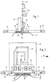
- FIGS. 1 and 2 The arrangement shown in FIGS. 1 and 2 in different side views has a soldering frame 10 known per se, which is guided past a soldering path in a horizontal position in a manner not shown, with a soldering wave 11 made of liquid solder coming into contact with from below which to soldering points of a circuit board 12 arrives. 1, the direction of movement of the soldering frame 10 extends into the image plane, while the direction of movement in FIG. 2 is indicated by an arrow A.
- the soldering frame 10 has a holder 13, only shown schematically, for the vertical positioning of the circuit board 12. Furthermore, a holder 14 for the horizontal positioning 10 of this circuit board 12 is provided.
- a further holder 16 is provided, which is arranged on the holder 13 for the circuit board 12. In principle, this holder 16 could also be attached to the printed circuit board 12 or directly to the soldering frame 10.
- Printed conductors 17 are arranged in a known manner on the printed circuit board 12, which in the exemplary embodiment shown form a specific configuration, which of course is subject to very large variations.
- These conductor tracks 17 represent connecting lines between electrical and electronic components 18, the connecting wires of which are inserted through holes in the printed circuit board 12 at connection points of the conductor tracks 17 and are or are soldered to these conductor tracks 17.
- These electrical components 18 are located on one side of the plate 12, while the vacuum fluorescence display 15 is located on the opposite side.
- the conductor tracks 17 lead to the connection of the vacuum fluorescence display 15 on soldering surfaces 19, which are located at the lower edge region of the printed circuit board 12.
- a corresponding number of solder connections 20, designed as connecting wires, of the vacuum fluorescent display 15 are bent in an S-shape toward the printed circuit board 12, the holder 16 being arranged relative to the holder 13 such that the ends of these solder connections 20 lie tangentially on the soldering surfaces 19.
- a protective mask 21 for thermal protection of the vacuum fluorescent display 15 is held below the vacuum fluorescent display on brackets 22, which in turn are attached to the holder 16.
- This bracket 22 may also be attached to other locations on the solder frame 10 or the circuit board 12.
- the solder connections 20 and the lower region of the printed circuit board 12 with the soldering areas 19 extend through this holder 22.
- the printed circuit board 12 is first inserted horizontally into the soldering frame 10, where it is held by the holders 14.
- the electrical components 18 are then placed in corresponding bores in the printed circuit board, for example by means of an automatic placement machine.
- the soldering frame 10 with the printed circuit board 12 is moved past a soldering shaft 11, through which the connecting wires projecting through the printed circuit board 12 and the conductor tracks in contact therewith are wetted and soldered to one another.
- the circuit board 12 is brought into the vertical position shown in FIGS. 1 and 2, where it is held by the holder 13. That too Vacuum fluorescence display 15 is brought into the corresponding vertical position in which its solder connections 20 rest against the soldering surfaces 19.
- soldering frame 10 is now moved again along a soldering path (not shown in more detail), the soldering connections 20 and the soldering areas 19 being wetted and soldered by a soldering shaft 11.
- the protective mask 21 protects the vacuum fluorescence display 15 and the other components 18 against thermal effects of the solder wave 11.
- the method according to the invention can be carried out in one operation, in which the soldering frame 10 is successively exposed to a soldering wave 11 and in between the transfer of the printed circuit board 12 from the horizontal to vertical position.
- the implementation can be done manually or, for example, by means of a robot arm. It is also possible to provide a pivotable holder for the printed circuit board 12 in the soldering frame 10, by means of which the printed circuit board 12 is automatically pivoted into the vertical position after the first soldering process.
- the vacuum fluorescence display 15 can also be added by means of a robot arm or an automatic placement machine.
- the method according to the invention is of course also suitable for other thermally sensitive components which are to be arranged on one side of the printed circuit board in relation to the other components and in which a manual electrical connection is possible.
- This method can be expanded by adding electrical components in the same way to the other sides of the circuit board be soldered, as was the case with the vacuum fluorescent display 15.
Abstract
Description
Die Erfindung betrifft ein Verfahren zum Anlöten eines thermisch empfindlichen Bauteils, wie eines Displays, an einer Leiterplatte, wobei dieses Bauteil an einer Seite der Leiterplatte und andere elektrische bzw. elektronische Bauteile an der gegenüberliegenden Seite der Leiterplatte anzuordnen sind, und das Anlöten der anderen elektrischen Bauteile mittels einer Lötstrecke durch Vorbeiführen der waagrecht in einem Lötrahmen befestigten Leiterplatte an einer Lötwelle erfolgt.The invention relates to a method for soldering a thermally sensitive component, such as a display, to a printed circuit board, this component being arranged on one side of the printed circuit board and other electrical or electronic components on the opposite side of the printed circuit board, and the soldering of the other electrical components Components are made by means of a soldering path by passing the printed circuit board horizontally fastened in a soldering frame to a soldering shaft.
Bei dem bekannten Lötverfahren wird eine zu bestückende Leiterplatte in waagrechter Position in einem Lötrahmen befestigt. Die Anschlußdrähte der anzulötenden Bauteile, wie Transistoren, Dioden, Widerstände, Kondensatoren und dergleichen, werden in entsprechende Bohrungen der Leiterplatte gesteckt, insbesondere mittels eines Bestückungsautomaten.Danach wird die Leiterplatte mit dem Lötrahmen an einer aus flüssigem Lot bestehenden Lötwelle vorbeigeführt, so daß die Unterseite der Leiterplatte benützt wird und die Anschlußdrähte an die entsprechenden Leiterbahnen gelötet werden. Die elektrischen Bauteile können bei einem anderen bekannten Verfahren auch an den entsprechenden Anschlußstellen der Leiterbahnen aufgeklebt und dann der Lötwelle ausgesetzt werden.In the known soldering method, a circuit board to be assembled is fastened in a horizontal position in a soldering frame. The connecting wires of the components to be soldered, such as transistors, diodes, resistors, capacitors and the like, are inserted into corresponding holes in the circuit board, in particular by means of an automatic assembly machine. The circuit board with the soldering frame is then guided past a soldering wave made of liquid solder, so that the underside the printed circuit board is used and the connecting wires are soldered to the corresponding conductor tracks. In another known method, the electrical components can also be connected to the corresponding ones The connection points of the conductor tracks are glued on and then exposed to the solder wave.
Soll ein Display, beispielsweise eine Vacuumfluorescenzanzeige ebenfalls an der Leiterplatte angelötet werden, so ist es aus Platzgründen häufig erforderlich, daß das Display auf der den übrigen Bauteilen gegenüberliegenden Seite der Leiterplatte angeordnet werden muß. An dieser Stelle wäre es jedoch beim automatischen Lötvorgang der heißen Lötwelle ausgesetzt, was bei derartigen thermisch empfindlichen Displays zu einer Zerstörung führen würde. In bekannter Weise wird daher das Display zunächst mit sehr langen Anschlußdrähten auf der Seite der übrigen Bauteile angeordnet, d.h. die Anschlußdrähte werden durch entsprechende Bohrungen der Leiterplatte hindurchgesteckt und der zuvor beschriebene Lötvorgang durchgeführt. Danach muß das Display mit den sehr langen Anschlußdrähten um die benachbarte Kante der Leiterplatte herumgebogen werden, damit das Display auf der den Bauteilen gegenüberliegenden Seite positioniert werden.If a display, for example a vacuum fluorescent display, is also to be soldered to the circuit board, it is often necessary for reasons of space that the display must be arranged on the side of the circuit board opposite the other components. At this point, however, it would be exposed to the hot solder wave during the automatic soldering process, which would lead to destruction in the case of such thermally sensitive displays. In a known manner, the display is therefore first arranged with very long connecting wires on the side of the other components, i.e. the connecting wires are inserted through corresponding holes in the circuit board and the previously described soldering process is carried out. Then the display with the very long connecting wires must be bent around the adjacent edge of the circuit board so that the display is positioned on the side opposite the components.
Der Nachteil des bekannten Verfahrens besteht darin, daß die sehr langen Anschlußdrähte mechanisch sehr leicht in ihrer Position verändert werden können und auch sehr schlecht ausrichtbar sind, so daß ein Einführen durch die Vielzahl von Leiterplattenbohrungen nur sehr schwer und umständlich durchführbar ist und ein vollautomatisches Verfahren daher nahezu ausscheidet. Durch das Umbiegen dieser Anschlußdrähte um die benachbarte Leiterplattenkante ist ein weiterer Verfahrensschritt erforderlich,die wiederum eine relativ komplizierte Handhabungstechnik erfordert. Darüber hinaus wirken sich die um die Kante herumgebogenen Anschlußdrähte häufig als störend aus und sind Anlaß zu Kurzschlüssen und Fehlfunktionen.The disadvantage of the known method is that the very long connecting wires can be changed mechanically very easily in their position and are also very difficult to align, so that insertion through the large number of printed circuit board holes is very difficult and cumbersome to carry out and is therefore a fully automatic method almost eliminated. By bending these connecting wires around the adjacent circuit board edge, a further process step is required, which in turn is a relatively complicated one Handling technology required. In addition, the connecting wires bent around the edge often have a disruptive effect and give rise to short circuits and malfunctions.
Eine Aufgabe der vorliegenden Erfindung besteht daher darin, derartige thermisch empfindliche Bauteile in einem einfach zu automatisierenden Verfahren so an einer Leiterplatte anzulöten, daß sie auf der den übrigen Bauteilen gegenüberliegenden Seite der Leiterplatte positioniert sind.It is therefore an object of the present invention to solder such thermally sensitive components to a printed circuit board in a process that is easy to automate in such a way that they are positioned on the side of the printed circuit board opposite the other components.
Diese Aufgabe wird erfindungsgemäß dadurch gelöst, daß in einem weiteren Schritt die Leiterplatte senkrecht auf dem Lötrahmen angeordnet wird, wobei die Lötanschlüsse des thermisch empfindlichen Bauteils in tangentialer Anlage mit im unteren randseitigen Bereich der Leiterplatte angeordneten Lötflächen der Leiterplatte gehalten werden, und daß der Lötrahmen an einer diese Lötflächen überstreichenden Lötwelle vorbeigeführt wird.This object is achieved in that the circuit board is arranged vertically on the soldering frame in a further step, the solder connections of the thermally sensitive component being held in tangential contact with soldering surfaces of the circuit board arranged in the lower edge-side region of the circuit board, and in that the soldering frame is on a solder wave is passed over these soldering areas.
Beim erfindungsgemäßen Verfahren können somit die übrigen Bauteile zunächst in der üblichen Weise verlötet werden. Dann muß die Leiterplatte lediglich in eine vertikale Position gebracht werden, wobei die Lötanschlüsse des thermisch empfindlichen Bauteils, beispielsweise eines Displays, an den entsprechenden Lötflächen anliegen. Beim Vorbeiführen an einer weiteren Lötwelle oder beim nochmaligen Vorbeiführen an der ersten Lötwelle wird dann lediglich der randseitige Bereich mit diesen Lötanschlüssen des Displays gelötet, während die übrigen Lötstellen nicht mehr in Kontakt mit der Lötwelle gelangen. Es muß also lediglich eine Vorrichtung zum vertikalen Aufrichten der Leiterplatte und zum Anlegen der Lötanschlüsse des thermisch empfindlichen Bauteils vorgesehen werden, so daß die gesamten Lötvorgänge in zwei Schritten in einem Verfahren durchgeführt werden können. Ein Durchstecken von Lötanschlüssen des thermisch empfindlichen Bauteils ist nicht mehr erforderlich, und die Ränder der Leiterplatte sind von allen Seiten frei zugänglich.In the method according to the invention, the remaining components can thus first be soldered in the usual way. Then the circuit board only has to be brought into a vertical position, the solder connections of the thermally sensitive component, for example a display, being in contact with the corresponding soldering surfaces. When passing another soldering wave or passing the first soldering wave again, only the edge area with these solder connections of the display is then soldered, while the other soldering points no longer come into contact with the soldering wave. So it has to only one device for vertical erection of the circuit board and for making the solder connections of the thermally sensitive component are provided, so that the entire soldering process can be carried out in two steps in one process. It is no longer necessary to push through the solder connections of the thermally sensitive component, and the edges of the circuit board are freely accessible from all sides.
Durch die in den Unteransprüchen aufgeführten Maßnahmen sind vorteilhafte Weiterbildungen und Verbesserungen des im Anspruch 1 angegebenen Verfahrens möglich.Advantageous further developments and improvements of the method specified in claim 1 are possible through the measures listed in the subclaims.
Die Drehung der Leiterplatte um im wesentlichen 90° auf dem Lötrahmen erfolgt in vorteilhafter Weise automatisch entweder durch eine schwenkbare Aufnahme am Lötrahmen oder durch Umstecken von der waagrechten Aufnahme in die senkrechte Aufnahme, beispielsweise durch einen Roboterarm. Dieses Umstecken kann selbstverständlich auch manuell durchgeführt werden.Advantageously, the circuit board is rotated essentially 90 ° on the soldering frame either automatically by a pivotable receptacle on the soldering frame or by repositioning from the horizontal receptacle into the vertical receptacle, for example by a robot arm. This change of course can of course also be carried out manually.
Das thermisch empfindliche Bauteil wird zweckmäßigerweise ebenfalls in eine entsprechende, seine Lötanschlüsse in die tangentiale Anlage an die Lötflächen der Leiterplatte haltende Halterung eingesetzt, um die mechanische Zuordnung zwischen Bauteil und Leiterplatte zu gewährleisten. Diese Halterung kann an der Leiterplatte oder am Lötrahmen angeordnet sein.The thermally sensitive component is also expediently inserted into a corresponding holder holding its solder connections in the tangential contact with the soldering surfaces of the printed circuit board in order to ensure the mechanical association between the component and the printed circuit board. This holder can be arranged on the circuit board or on the soldering frame.
Das als Display ausgebildete Bauteil wird im wesentlichen parallel zur Leiterplatte angeordnet, wobei die Lötanschlüsse zuvor zur Anlage an die Lötflächen der Leiterplatte im wesentlichen S-förmig vorgerichtet wurden. Das Display kann entweder mit derart vorgerichteten Lötanschlüssen bezogen werden oder das Vorrichten erfolgt in einem gesonderten Arbeitsgang.The component designed as a display is arranged essentially parallel to the circuit board, with the solder connections were previously prepared in an essentially S-shaped manner for contact with the soldering surfaces of the printed circuit board. The display can either be covered with pre-arranged solder connections or set-up takes place in a separate operation.
Zum thermischen Schutz ist zweckmäßigerweise eine Maske unterhalb des thermisch empfindlichen Bauteils angeordnet, durch die der untere Bereich der Leiterplatte mit den Lötflächen sowie die Lötanschlüsse des thermisch empfindlichen Bauteils hindurchreichen. Hierdurch wird verhindert, daß die Lötwelle in Kontakt mit dem thermisch empfindlichen Bauteil selbst gelangen kann.For thermal protection, a mask is expediently arranged below the thermally sensitive component, through which the lower region of the printed circuit board with the soldering areas and the solder connections of the thermally sensitive component extend. This prevents the solder wave from coming into contact with the thermally sensitive component itself.
Zur Erläuterung des Verfahrens ist eine auf einem Lötrahmen angeordnete Leiterplatte in der Zeichnung dargestellt und in der nachfolgenden Beschreibung näher erläutert. Es zeigen:
- Fig. 1
- eine vertikal auf einem Lötrahmen angeordnete Leiterplatte in einer Ansicht auf die Schmalseite und
- Fig. 2
- eine um 90° versetzte Seitenansicht auf eine Breitseite der Leiterplatte.
- Fig. 1
- a vertically arranged on a soldering frame in a view of the narrow side and
- Fig. 2
- a side view offset by 90 ° on a broad side of the circuit board.
Die in den Fig. 1 und 2 in verschiedenen Seitenansichten dargestellte Anordnung weist einen an sich bekannten Lötrahmen 10 auf, der in nicht näher dargestellter Weise an einer Lötstrecke in waagrechter Position vorbeigeführt wird, wobei von unten her eine Lötwelle 11 aus flüssigem Lot in Kontakt mit den zu lötenden Stellen einer Leiterplatte 12 gelangt. Die Bewegungsrichtung des Lötrahmens 10 verläuft gemäß Fig. 1 in die Bildebene hinein, während die Bewegungsrichtung in Fig. 2 durch einen Pfeil A gekennzeichnet ist.The arrangement shown in FIGS. 1 and 2 in different side views has a soldering
Der Lötrahmen 10 besitzt einen nur schematisch dargestellte Halterung 13 zur vertikalen Positionierung der Leiterplatte 12. Weiterhin ist eine Halterung 14 zur horizontalen Positionierung 10 dieser Leiterplatte 12 vorgesehen.The soldering
Zur Positionierung eines Vacuumfluorescenzdisplays 15 parallel zur vertikalpositionierten Leiterplatte 12 ist eine weitere Halterung 16 vorgesehen, die an der Halterung 13 für die Leiterplatte 12 angeordnet ist. Prinzipiell könnte diese Halterung 16 auch an der Leiterplatte 12 oder direkt am Lötrahmen 10 angebracht sein.To position a vacuum
Auf der Leiterplatte 12 sind in bekannter Weise Leiterbahnen 17 angeordnet, die im dargestellten Ausführungsbeispiel eine bestimmte Konfiguration bilden, die selbstverständlich sehr großen Variationen unterliegt. Diese Leiterbahnen 17 stellen Verbindungsleitungen zwischen elektrischen und elektronischen Bauteilen 18 dar, deren Anschlußdrähte durch Bohrungen in der Leiterplatte 12 an Anschlußstellen der Leiterbahnen 17 hindurchgesteckt und mit diesen Leiterbahnen 17 verlötet sind bzw. verlötet werden. Diese elektrischen Bauteile 18 befinden sich an einer Seite der Platte 12, während sich das Vacuumfluoresvcenzdisplay 15 an der gegenüberliegenden Seite befindet. Die Leiterbahnen 17 münden zum Anschluß des Vacuumfluorescenzdisplays 15 an Lötflächen 19, die sich am unteren Randbereich der Leiterplatte 12 befinden. Eine entsprechende Anzahl von als Anschlußdrähte ausgebildeten Lötanschlüssen 20 des Vacuumfluorescenzdisplays 15 sind S-förmig zur Leiterplatte 12 hin gebogen, wobei die Halterung 16 relativ zur Halterung 13 so angeordnet ist, daß die Enden dieser Lötanschlüsse 20 tangential an den Lötflächen 19 anliegen.Printed
Unterhalb des Vacuumfluorescenzdisplays ist eine Schutzmaske 21 zum thermischen Schutz des Vacuumfluorescenzdisplays 15 an Halterungen 22 gehalten, die ihrererseits an der Halterung 16 befestigt sind. Diese Halterung 22 kann ebenfalls an anderen Stellen desLötrahmens 10 oder der Leiterplatte 12 befestigt sein. Die Lötanschlüsse 20 und der untere Bereich der Leiterplatte 12 mit den Lötflächen 19 reichen durch diese Halterung 22 hindurch.A
Für das erfindungsgemäße Lötverfahren wird zunächst die Leiterplatte 12 horizontal in den Lötrahmen 10 eingelegt, wo sie durch die Halterungen 14 gehalten wird. Danach werden die elektrischen Bauteile 18 in entsprechende Bohrungen der Leiterplatte angesetzt, beispielsweise durch einen Bestückungsautomaten. Danach wird der Lötrahmen 10 mit der bestückten Leiterplatte 12 an einer Lötwelle 11 vorbeibewegt, durch die die durch die Leiterplatte 12 hindurchragenden Anschlußdrähte und die damit in Kontakt stehenden Leiterbahnen benetzt und miteinander verlötet werden. Danach wird die Leiterplatte 12 in die in den Fig. 1 und 2 dargestellte vertikale Position gebracht, wo sie durch die Halterung 13 gehalten wird. Auch das Vacuumfluorescenzdisplay 15 wird in die entsprechende vertikale Position gebracht, in der seine Lötanschlüsse 20 an den Lötflächen 19 anliegen. Nun wird der Lötrahmen 10 erneut entlang einer nicht näher dargestellten Lötstrecke bewegt, wobei die Lötanschlüsse 20 und die Lötflächen 19 von einer Lötwelle 11 benetzt und verlötet werden. Die Schutzmaske 21 schützt das Vaccumfluorescenzdisplay 15 und die übrigen Bauteile 18 gegen thermische Einwirkungen der Lötwelle 11.For the soldering method according to the invention, the printed
Die Durchführung des erfindungsgemäßen Verfahrens kann in einem Arbeitsvorgang erfolgen, bei dem der Lötrahmen 10 nacheinander jeweils einer Lötwelle 11 ausgesetzt wird und wobei dazwischen das Umsetzen der Leiterplatte 12 von der
horizontalen in die vertikale Position erfolgt. Das Umsetzen kann manuell oder beispielsweise mittels eines Roboterarms erfolgen. Es ist auch möglich, im Lötrahmen 10 eine schwenkbare Halterung für die Leiterplatte 12 vorzusehen, durch die die Leiterplatte 12 nach dem ersten Lötvorgang automatisch in die vertikale Lage geschwenkt wird. Das Hinzufügen des Vacuumfluorescenzdisplays 15 kann ebenfalls mittels eines Roboterarms bzw. eines Bestückungsautomaten erfolgen.The method according to the invention can be carried out in one operation, in which the soldering
horizontal to vertical position. The implementation can be done manually or, for example, by means of a robot arm. It is also possible to provide a pivotable holder for the printed
Das erfindungsgemäße Verfahren eignet sich selbstverständlich auch für andere thermisch empfindliche Bauteile, die an einer Seite der Leiterplatte gegenüber den übrigen Bauteilen angeordnet werden sollen , und bei denen ein handseitiger elektrischer Anschluß möglich ist. Dieses Verfahren läßt sich noch dadurch erweitern, daß auch an den übrigen Seiten der Leiterplatte noch nachträglich elektrische Bauteile in derselben Weise angelötet werden, wie dies beim Vacuumfluorescenzdisplay 15 der Fall war.The method according to the invention is of course also suitable for other thermally sensitive components which are to be arranged on one side of the printed circuit board in relation to the other components and in which a manual electrical connection is possible. This method can be expanded by adding electrical components in the same way to the other sides of the circuit board be soldered, as was the case with the
Claims (7)
Applications Claiming Priority (2)
| Application Number | Priority Date | Filing Date | Title |
|---|---|---|---|
| DE4232600 | 1992-09-29 | ||
| DE4232600A DE4232600A1 (en) | 1992-09-29 | 1992-09-29 | Process for soldering a thermally sensitive component, such as a display, to a printed circuit board |
Publications (2)
| Publication Number | Publication Date |
|---|---|
| EP0590512A1 true EP0590512A1 (en) | 1994-04-06 |
| EP0590512B1 EP0590512B1 (en) | 1995-10-25 |
Family
ID=6469114
Family Applications (1)
| Application Number | Title | Priority Date | Filing Date |
|---|---|---|---|
| EP93115319A Expired - Lifetime EP0590512B1 (en) | 1992-09-29 | 1993-09-23 | Method of soldering a heat sensitive component, e.g a display, to a printed circuit board |
Country Status (3)
| Country | Link |
|---|---|
| EP (1) | EP0590512B1 (en) |
| DE (2) | DE4232600A1 (en) |
| TR (1) | TR27258A (en) |
Cited By (3)
| Publication number | Priority date | Publication date | Assignee | Title |
|---|---|---|---|---|
| EP1175131A2 (en) * | 2000-06-19 | 2002-01-23 | Matsushita Electric Industrial Co., Ltd. | Compact fluorescent lamp |
| US6411524B1 (en) * | 2000-10-04 | 2002-06-25 | General Electric Company | Dual planar printed wiring board for compact fluorescent lamp |
| EP3955711A1 (en) * | 2020-08-10 | 2022-02-16 | Vestel Elektronik Sanayi ve Ticaret A.S. | Electronic system and method |
Families Citing this family (2)
| Publication number | Priority date | Publication date | Assignee | Title |
|---|---|---|---|---|
| JP2665191B2 (en) * | 1995-04-28 | 1997-10-22 | 静岡日本電気株式会社 | LCD holding bracket |
| CN114430624B (en) * | 2020-10-29 | 2024-03-15 | 鹏鼎控股(深圳)股份有限公司 | Circuit board manufacturing method and circuit board |
Citations (1)
| Publication number | Priority date | Publication date | Assignee | Title |
|---|---|---|---|---|
| FR2571920A1 (en) * | 1984-10-11 | 1986-04-18 | Diehl Gmbh & Co | ARRANGEMENT FOR MOUNTING AN ELECTRONIC DISPLAY |
-
1992
- 1992-09-29 DE DE4232600A patent/DE4232600A1/en not_active Withdrawn
-
1993
- 1993-09-23 EP EP93115319A patent/EP0590512B1/en not_active Expired - Lifetime
- 1993-09-23 DE DE59300820T patent/DE59300820D1/en not_active Expired - Lifetime
- 1993-09-29 TR TR00866/93A patent/TR27258A/en unknown
Patent Citations (1)
| Publication number | Priority date | Publication date | Assignee | Title |
|---|---|---|---|---|
| FR2571920A1 (en) * | 1984-10-11 | 1986-04-18 | Diehl Gmbh & Co | ARRANGEMENT FOR MOUNTING AN ELECTRONIC DISPLAY |
Cited By (4)
| Publication number | Priority date | Publication date | Assignee | Title |
|---|---|---|---|---|
| EP1175131A2 (en) * | 2000-06-19 | 2002-01-23 | Matsushita Electric Industrial Co., Ltd. | Compact fluorescent lamp |
| EP1175131A3 (en) * | 2000-06-19 | 2003-03-12 | Matsushita Electric Industrial Co., Ltd. | Compact fluorescent lamp |
| US6411524B1 (en) * | 2000-10-04 | 2002-06-25 | General Electric Company | Dual planar printed wiring board for compact fluorescent lamp |
| EP3955711A1 (en) * | 2020-08-10 | 2022-02-16 | Vestel Elektronik Sanayi ve Ticaret A.S. | Electronic system and method |
Also Published As
| Publication number | Publication date |
|---|---|
| EP0590512B1 (en) | 1995-10-25 |
| DE4232600A1 (en) | 1994-03-31 |
| DE59300820D1 (en) | 1995-11-30 |
| TR27258A (en) | 1994-12-22 |
Similar Documents
| Publication | Publication Date | Title |
|---|---|---|
| DE10211647B4 (en) | Method for loading and soldering a printed circuit board | |
| DE3790315C2 (en) | ||
| DE2242337C2 (en) | Device for holding circuit cards | |
| DE69732045T2 (en) | Method and device for shielding electronic components on a printed circuit board | |
| DE3146796A1 (en) | "ENCLOSURE FOR A SEMICONDUCTOR CHIP WITH INTEGRATED CIRCUIT" | |
| DE1952569A1 (en) | Carrier for electrical components and integrated circuits | |
| DE3511722A1 (en) | ELECTROMECHANICAL ASSEMBLY FOR INTEGRATED CIRCUIT MATRICES | |
| WO1997044823A1 (en) | Substrate for a semiconductor chip | |
| EP0464232A1 (en) | Solder connector and process for making an electrical circuit with this solder connector | |
| EP2361001A1 (en) | Soldering mask for wave soldering and method for selective soldering of individual components of a circuit board in a wave soldering machine | |
| DE1791024B1 (en) | CIRCUIT BOARD AND METHOD OF MANUFACTURING IT | |
| EP1393604B1 (en) | Printed circuit board comprising a contact sleeve that is mounted thereon | |
| EP0613331B1 (en) | Method of attaching a hybrid circuit on a pcb | |
| DE60005047T2 (en) | DEVICE AND METHOD FOR CONNECTING PCBS BY SOLDERED OVERLAP CONNECTIONS | |
| EP0590512B1 (en) | Method of soldering a heat sensitive component, e.g a display, to a printed circuit board | |
| DE2348630B2 (en) | Device for protecting MOS components against damage caused by electrostatic charges | |
| DE19527398A1 (en) | Process for soldering components on a carrier film | |
| EP0306930A2 (en) | Conductor tracks with connection points for an electronic component comprising a plurality of terminals, arranged on a circit board | |
| DE4402545A1 (en) | Method for the formation of discrete solder points on corresponding contact connection surfaces on a printed circuit board | |
| DE2223195C3 (en) | Method and device for the non-thermal loosening of mechanical connections | |
| EP0219517B1 (en) | Thermoplastic soldering material, process and device | |
| DE19840234C1 (en) | Printed circuit board screening soldering method e.g. for cordless telephones or mobile radio apparatus | |
| DE4204882C2 (en) | Device and method for equipping surface-mountable components with small contact distances | |
| DE2708776C2 (en) | Circuit arrangement with hybrid components | |
| DD226722A1 (en) | TEMPLATE FOR POSITIONING AND FIXING OF SEPARABLE COMPONENTS |
Legal Events
| Date | Code | Title | Description |
|---|---|---|---|
| PUAI | Public reference made under article 153(3) epc to a published international application that has entered the european phase |
Free format text: ORIGINAL CODE: 0009012 |
|
| AK | Designated contracting states |
Kind code of ref document: A1 Designated state(s): DE FR GB IT |
|
| 17P | Request for examination filed |
Effective date: 19940301 |
|
| 17Q | First examination report despatched |
Effective date: 19940707 |
|
| GRAA | (expected) grant |
Free format text: ORIGINAL CODE: 0009210 |
|
| AK | Designated contracting states |
Kind code of ref document: B1 Designated state(s): DE FR GB IT |
|
| GBT | Gb: translation of ep patent filed (gb section 77(6)(a)/1977) |
Effective date: 19951024 |
|
| REF | Corresponds to: |
Ref document number: 59300820 Country of ref document: DE Date of ref document: 19951130 |
|
| ITF | It: translation for a ep patent filed |
Owner name: GUZZI E RAVIZZA S.R.L. |
|
| ET | Fr: translation filed | ||
| PLBE | No opposition filed within time limit |
Free format text: ORIGINAL CODE: 0009261 |
|
| STAA | Information on the status of an ep patent application or granted ep patent |
Free format text: STATUS: NO OPPOSITION FILED WITHIN TIME LIMIT |
|
| 26N | No opposition filed | ||
| REG | Reference to a national code |
Ref country code: GB Ref legal event code: IF02 |
|
| PGFP | Annual fee paid to national office [announced via postgrant information from national office to epo] |
Ref country code: GB Payment date: 20120823 Year of fee payment: 20 |
|
| PGFP | Annual fee paid to national office [announced via postgrant information from national office to epo] |
Ref country code: DE Payment date: 20120707 Year of fee payment: 20 Ref country code: FR Payment date: 20120926 Year of fee payment: 20 Ref country code: IT Payment date: 20120912 Year of fee payment: 20 |
|
| REG | Reference to a national code |
Ref country code: DE Ref legal event code: R071 Ref document number: 59300820 Country of ref document: DE |
|
| REG | Reference to a national code |
Ref country code: DE Ref legal event code: R071 Ref document number: 59300820 Country of ref document: DE |
|
| REG | Reference to a national code |
Ref country code: GB Ref legal event code: PE20 Expiry date: 20130922 |
|
| PG25 | Lapsed in a contracting state [announced via postgrant information from national office to epo] |
Ref country code: DE Free format text: LAPSE BECAUSE OF EXPIRATION OF PROTECTION Effective date: 20130924 |
|
| PG25 | Lapsed in a contracting state [announced via postgrant information from national office to epo] |
Ref country code: GB Free format text: LAPSE BECAUSE OF EXPIRATION OF PROTECTION Effective date: 20130922 |