EP0589103A1 - Image projection method and semiconductor device manufacturing method using the same - Google Patents
Image projection method and semiconductor device manufacturing method using the same Download PDFInfo
- Publication number
- EP0589103A1 EP0589103A1 EP92308599A EP92308599A EP0589103A1 EP 0589103 A1 EP0589103 A1 EP 0589103A1 EP 92308599 A EP92308599 A EP 92308599A EP 92308599 A EP92308599 A EP 92308599A EP 0589103 A1 EP0589103 A1 EP 0589103A1
- Authority
- EP
- European Patent Office
- Prior art keywords
- pupil
- light source
- longitudinal
- pattern
- sides
- Prior art date
- Legal status (The legal status is an assumption and is not a legal conclusion. Google has not performed a legal analysis and makes no representation as to the accuracy of the status listed.)
- Granted
Links
Images


Classifications
-
- G—PHYSICS
- G03—PHOTOGRAPHY; CINEMATOGRAPHY; ANALOGOUS TECHNIQUES USING WAVES OTHER THAN OPTICAL WAVES; ELECTROGRAPHY; HOLOGRAPHY
- G03F—PHOTOMECHANICAL PRODUCTION OF TEXTURED OR PATTERNED SURFACES, e.g. FOR PRINTING, FOR PROCESSING OF SEMICONDUCTOR DEVICES; MATERIALS THEREFOR; ORIGINALS THEREFOR; APPARATUS SPECIALLY ADAPTED THEREFOR
- G03F7/00—Photomechanical, e.g. photolithographic, production of textured or patterned surfaces, e.g. printing surfaces; Materials therefor, e.g. comprising photoresists; Apparatus specially adapted therefor
- G03F7/70—Microphotolithographic exposure; Apparatus therefor
- G03F7/70058—Mask illumination systems
- G03F7/70091—Illumination settings, i.e. intensity distribution in the pupil plane or angular distribution in the field plane; On-axis or off-axis settings, e.g. annular, dipole or quadrupole settings; Partial coherence control, i.e. sigma or numerical aperture [NA]
- G03F7/701—Off-axis setting using an aperture
-
- G—PHYSICS
- G03—PHOTOGRAPHY; CINEMATOGRAPHY; ANALOGOUS TECHNIQUES USING WAVES OTHER THAN OPTICAL WAVES; ELECTROGRAPHY; HOLOGRAPHY
- G03F—PHOTOMECHANICAL PRODUCTION OF TEXTURED OR PATTERNED SURFACES, e.g. FOR PRINTING, FOR PROCESSING OF SEMICONDUCTOR DEVICES; MATERIALS THEREFOR; ORIGINALS THEREFOR; APPARATUS SPECIALLY ADAPTED THEREFOR
- G03F7/00—Photomechanical, e.g. photolithographic, production of textured or patterned surfaces, e.g. printing surfaces; Materials therefor, e.g. comprising photoresists; Apparatus specially adapted therefor
- G03F7/70—Microphotolithographic exposure; Apparatus therefor
- G03F7/70216—Mask projection systems
- G03F7/70241—Optical aspects of refractive lens systems, i.e. comprising only refractive elements
Definitions
- This invention relates to an image projection method and a semiconductor device manufacturing method using the same. More particularly, the invention is concerned with an improved image projection method suitable for forming on a wafer a circuit pattern of a linewidth not greater than 0.5 micron and with an improved semiconductor device manufacturing method based on such an image projection method.
- each semiconductor device such as IC, LSI or the like has been increased more and more and, along this, the fine processing technique has been improved considerably.
- the exposure technique which is the major processing technique in semiconductor device manufacturing processes has been advanced into a submicron region, with manufacture of 1 mega-DRAM.
- a representative exposure apparatus therefor is a reduction projection exposure apparatus, called a stepper. It is not an overestimation to say that the resolution of such a stepper determines the future of semiconductor devices.
- NA numerical aperture
- a projection optical system reduction lens system
- enlarging the NA results in a decrease of the depth of focus, causing a difficulty of forming on a wafer an image of good contrast.
- recently adopted method for enhancing the resolution is to use shorter wavelengths for the exposure light, such as by using i-line light (365 nm) or KrF excimer laser light (248 nm) in place of g-line light (436 nm). This relies upon an effect that, if the depth of focus allowable in the optical system is considered as constant, the resolution increase in inverse proportion to the root of the wavelength.
- a method of improving the resolution of a stepper by illuminating a reticle in a specific manner is that a reticle is illuminated with the light which forms a ring-like effective light source (a virtual light source formed by zeroth order light) at a pupil of a projection optical system.
- a ring-like effective light source a virtual light source formed by zeroth order light
- diffraction light (zeroth and first orders) produced by a circuit pattern of a reticle can be projected onto the pupil of the projection optical system.
- the light that forms a ring-like effective light source can be supplied by forming a ring-like secondary light source at a position within the illumination system which is optically conjugate with the pupil of the projection optical system.
- the "side" of the effective light source means the side that defines the basic configuration of the effective light source. It comprehends not only the one provided by connected straight lines as viewed microscopically but also the one which is provided by connected curved lines as viewed microscopically but the connections of which are along a predetermined straight line when viewed macroscopically.
- the inside peripheral configuration of the ring-like effective light source is mainly defined by those sides extending in the aforementioned directions, and the sides of the inside peripheral configuration includes a first pair of sides which are symmetrical with respect to an axis parallel to the direction of elongation of a transverse pattern, extending through the center of the pupil, and a second pair of sides which are symmetrical with respect to an axis parallel to the direction of elongation of a longitudinal pattern, extending through the center of the pupil.
- the peripheral configuration of the ring-like effective light source is mainly defined by those sides extending in the aforementioned directions, and the sides of the peripheral configuration includes a third pair of sides which are symmetrical with respect to an axis parallel to a transverse pattern, extending through the center of the pupil, and a fourth pair of sides which are symmetrical with respect to an axis parallel to a longitudinal pattern, extending through the center of the pupil.
- the illumination uses the light which defines an effective light source such as described, it is possible to improve the depth of focus of a projection optical system, in respect to longitudinal and transverse patterns, as compared with the illumination using the light which defines a circular effective light source of conventional type.
- the light that defines an effective light source as described can be supplied by providing a primary or secondary light source of a shape analogous to that of the effective light source, at a position optically conjugate with the pupil of the projection optical system.
- a semiconductor device manufacturing method wherein a circuit pattern is illuminated and wherein diffraction light caused by the circuit pattern is projected on a pupil of a projection optical system and an image of the circuit pattern is projected on a wafer, whereby the image of the circuit pattern is transferred onto the wafer, and specifically wherein the circuit pattern is illuminated with light from a secondary light source of a predetermined shape so as to assure that zeroth order diffraction light and first order diffraction light caused by longitudinal and transverse patterns, constituting the circuit pattern, is distributed along a substantially rectangular configuration about the center of the pupil.
- Figure 1 is a schematic view of a projection exposure apparatus to which a method of the present invention is applied.
- Figure 2 is a schematic view of an effective light source on a pupil in the apparatus of Figure 1.
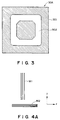
- Figure 3 is a schematic view of an aperture stop in an illumination optical system of the Figure 1 apparatus.
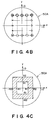
- Figures 4A - 4C are schematic views for explaining the advantages of the effective light source applied to the Figure 1 apparatus, wherein Figure 4A illustrates longitudinal and transverse patterns, Figure 4B illustrates preferable distribution of diffraction light upon the pupil, and Figure 4C illustrates the basic form of the effective light source that produces the diffraction light distribution of Figure 4B.
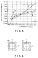
- Figure 5 is a graph showing the relationship between the linewidth of a bar chart image and the depth of focus of a projection lens system, based on the results of computer simulation made on the imaging characteristic in accordance with an image projection method, for forming a rectangular ring-like effective light source of Figure 4C, and an image projection method for forming a circular effective light source.
- Figure 6 is a schematic view of variations of the effective light source of the present invention.
- Figure 7 is a sectional view of an optical integrator of the Figure 1 apparatus.
- Figure 8 is a schematic view of an effective light source on the pupil of the Figure 1 apparatus, as can be seen practically.
- Figure 1 shows a projection exposure apparatus for manufacturing semiconductor devices in accordance with a method of the present invention.
- At M is a reticle having a circuit pattern formed thereon.
- Denoted at W is a wafer which is coated with a resist.
- Denoted at 10 is an optical axis of the apparatus; at 20 is a light source (primary light source); at 30 is an illumination optical system for directing light from the light source 20 to the reticle M; and at 30A is an aperture stop of the illumination optical system 30.
- the aperture stop 30A is placed in the neighbourhood of the light exit surface of an optical integrator (fly's eye lens), not shown, of the illumination optical system 30, and it cooperates with the optical integrator to form a ring-like secondary light source at its opening
- Denoted at 40 is a reticle stage for supporting the reticle M
- at 50 is a projection lens system for projecting a reduced image of the circuit pattern of the reticle M uniformly illuminated with the light from the ring-like secondary light source of the illumination optical system 30
- denoted at 50A is an aperture stop of the projection lens system 50.
- the aperture stop 50A defines the pupil of the projection lens system 50.
- the position of the stop 50 is taken as the position of the pupil.
- Denoted at 60 is a wafer stage for supporting the wafer W, and this stage 60 supports the wafer W so as to bring the wafer W surface into alignment with the imaging plane of the circuit pattern of the reticle M by the projection lens system 50.
- the reticle M When in the above-described structure the reticle M is illuminated by using the light source 20 and the illumination optical system 30, diffraction light caused by the circuit pattern of the reticle M, mainly consisting of a combination of longitudinal and transverse patterns), is received by the opening of the stop 50A of the projection lens system 50.
- the projection lens system 50 projects an image of the circuit pattern of the reticle M onto the wafer W, whereby the image of the circuit pattern is transferred to the resist of the wafer W.
- semiconductor chips can be manufactured from the wafer W.
- the position of the stop 30A of the illumination optical system 30 and the position of the stop 50A of the projection lens system 50 are placed in an optically conjugate relationship with each other, and an image of the opening of the stop 30A (i.e. secondary light source) is projected upon the opening of the stop 50A of the projection lens system 50.
- an image of the opening of the stop 30A i.e. secondary light source
- the shape or size of the image of the opening of the stop 30A to be formed on the opening of the stop 50A namely, the shape or size of the effective light source
- the opening of the stop 50A has a circular shape.
- FIG 2 is a schematic view of the effective light source defined on the pupil (hereinafter "pupil 50A") of the projection lens system 50 of Figure 1
- Figure 3 is a front view of the stop 30A of the illumination optical system 30 of the Figure 1 apparatus.
- the pupil 50A of the projection lens system 50 as well as the effective light source are illustrated with reference to an x-y coordinate system with its origin coinciding with the center of the pupil 50A.
- the x axis of this x-y coordinate system corresponds to the direction of elongation of a transverse pattern (linear pattern extending transversely or laterally) of the reticle M, while the y axis of the x-y coordinate system corresponds to the direction of elongation of a longitudinal pattern (linear pattern extending longitudinally) of the reticle M.
- the optical integrator of the Figure 1 apparatus comprises a fly's eye lens consisting of a combination of lens elements as illustrated in the sectional view of Figure 7, the effective light source as can be practically observed upon the pupil 50A is such as shown in Figure 8.
- This effective light source is figured by curved lines defined by connected peripheral configurations of images of the inside and outside lens elements, but here the peripheral configuration of the effective light source is taken as one figured by lines extending along the array of the images of the inside and outside lens elements.
- a ring-like effective light source having sides extending along the directions of elongation of the longitudinal and transverse patterns of the reticle M, is formed on the pupil 50A.
- This effective light source comprises a ring-like effective light source whose inside and outside peripheral configurations are approximately rectangular.
- the stop 30A of the Figure 1 apparatus comprises a stop member having a ring-like opening 302 defined by a light blocking portion 301, the opening 302 having inside and outside peripheral configurations of approximately rectangular shape, for defining the effective light source of Figure 2 upon the pupil 50A.
- a ring-like effective light source having inside and outside peripheral configurations of approximately rectangular shape, is defined. While no x-y coordinate system is illustrated in Figure 3, from the comparison with Figure 2 it will be clear that the origin coincides with the center (optical axis) of the opening 30, that the transverse direction in the drawing corresponds to the x axis extending through the origin and that the longitudinal direction in the drawing corresponds to the y axis extending through the origin.
- the reticle M is so illuminated that an image of the opening of the stop 30A shown in Figure 3 is projected on the pupil 50A of the projection lens system 50, by which an approximately rectangular ring-like effective light source is formed on the pupil, while on the other hand an image of the circuit pattern of the reticle M is projected on the wafer W.
- an image of the circuit pattern of the reticle M is projected on the wafer W.
- the symbols o, ⁇ , ⁇ and X denote zeroth order diffraction light and first order diffraction light. More specifically, the symbols o and ⁇ denote the pair of diffraction lights produced by the pattern M1, wherein, if the symbol o depicts the zeroth order light, the symbol ⁇ depicts the first order light, whereas if the symbol ⁇ depicts the zeroth order light, the symbol o depicts the first order light.
- the symbols ⁇ and X denote the pair of diffraction lights produced by the pattern M2, wherein, if the symbol ⁇ depicts the zeroth order light, the symbol X depicts the first order light, whereas if the symbol X depicts the zeroth order light, the symbol ⁇ depicts the first order light.
- These diffraction lights are distributed on the pupil 50A so as to define rectangular peripheral configurations. Such distribution of diffraction light may be accomplished by forming on the pupil 50A a ring-like effective light source such as shown in Figure 4C, having inside and outside peripheral configurations of square shape and having its center coinciding with the center (optical axis) of the pupil.
- an effective light source having inside and outside peripheral configurations of square shape or rectangular shape or, alternatively, of a deformed shape of it, is provided.
- Figure 5 shows the comparison results of computer simulation made on the imaging characteristic, according to the image projection method wherein a rectangular ring-like effective light source of Figure 4C is formed and according to the image projection method wherein a circular ring-like effective light source is formed.
- a projection lens of a numerical aperture (NA) of 0.52 and a bar chart of one dimensional line-and-space, having five lines, were selected, and the relationship between the linewidth of the bar char image and the depth of focus at a contrast 7% was examined under the condition that the bar chart image was imaged by using i-line (wavelength 365 nm).
- NA numerical aperture
- curve (1) depicts the characteristic of longitudinal and transverse patterns when an effective light source of Gaussian intensity distribution, having a highest intensity at the pupil center, is formed.
- Curve (2) depicts the characteristic of longitudinal and transverse patterns when a circular ring-like effective light source is formed.
- Curve (3) depicts the characteristic of longitudinal and transverse patterns when a rectangular ring-like effective light source is formed.
- Curve (4) depicts the characteristic of inclined (45 deg.) patterns when a rectangular ring-like effective light source is formed.
- the size of the circular ring-like effective light source is such that, if the radius of the pupil is taken as 1, the radius of the inside circular peripheral configuration is 0.4 while the radius of the outside peripheral configuration is 0.8.
- the imaging characteristic of the inclined 45 deg. patterns when a rectangular ring-like effective light source is formed and the imaging characteristic of the longitudinal and transverse patterns when a circular ring-like effective light source is formed are substantially the same.
- the imaging characteristic of the longitudinal and transverse patterns when a rectangular ring-like effective light source is formed is superior to that of the longitudinal and transverse patterns where an effective light source of Gaussian intensity distribution is formed or to that of the longitudinal and transverse patterns where a circular effective light source is formed; and the depth of focus to the longitudinal and transverse patterns is improved considerably.
- the limit resolution to longitudinal and transverse patterns in a case where a circular effective light source is formed is 0.44 micron
- the limit resolution to longitudinal and transverse patterns in a case where a rectangular ring-like effective light source is formed is 0.37 micron.
- preferable forms of such a rectangular ring-like effective light source are those such as shown in Figure 4C, or those having a similar shape wherein, when standardization is made while taking the radius of the pupil as 1, the inside and outside peripheral configurations of the effective light source are in the ranges of 0.1 ⁇ R1 ⁇ 0.65 and 0.25 ⁇ R2 ⁇ 0.71.
- the stop 30A shown in Figure 3 is used to provide a secondary light source having inside and outside peripheral configurations of square-like shape, and an effective light source of a shape analogous to such secondary light source is defined on the pupil 50A.
- an effective light source of a shape analogous to such secondary light source is defined on the pupil 50A.
- at least one of the inside and outside peripheral configurations includes a side which extends in the direction of elongation of a longitudinal or transverse pattern.
- the lines connecting the gravity centers with respect to the radial direction (such as shown by a broken line in Figure 2) take an approximately rectangular shape and, in respect to the imaging of longitudinal and transverse patterns, it is possible to obtain a depth of focus greater than that attainable with a circular effective light source.
- the stop 30A of the illumination optical system of the Figure 1 apparatus may be replaced by a stop member having an opening of a shape like the hatched portion in Figure 6A or 6B.
- the stop 30A of Figure 3 While in the stop 30A of Figure 3 the portion other than the opening 302, namely, the light blocking portion 301 is arranged to fully block light, the stop may be modified so that light is partially transmitted through this portion. What is important is that the intensity of light passing through the opening 302 is sufficiently higher than that passing through the remaining portion, and that, when an image of the opening 302 is formed on the pupil 50A, an effective light source with inside and outside peripheral configurations at least one of which includes a side extending in the direction of elongation of a longitudinal or transverse pattern, is defined on the pupil 50A.
- the secondary light source or the effective light source has a uniform intensity distribution.
- a fly's eye lens having lens elements of circular cross-section such as shown in Figure 7 is used.
- a fly's eye lens comprising a combination of lens elements having a square cross-section or a hexagonal cross-section, may be used.
- the stop 30A is disposed adjacent to the light exit surface of the optical integrator, it may be placed in the neighbourhood of the light entrance surface of the optical integrator.
- a rectangular ring-like secondary light source is defined on the light entrance surface of the optical integrator, and an image of such secondary light source is projected on the pupil 50A of the projection lens system 50.
- a lens element or elements which are at the central portion of the optical integrator do not contribute to the definition of the ring-like secondary light source and, therefore, such an optical integrator not having such lens element or elements is possible to use.
- the light receiving surface of such central lens element or elements of the optical integrator may be covered by a light blocking film or the like.
- the structure of the illumination optical system may be modified in various ways, known in the art. Further, as the light source 20, an ultra-high pressure Hg lamp or an excimer laser may be used, for example.
- a projection lens system is used to project an image of the pattern of the reticle M.
- the invention is applicable also to an apparatus using a projection mirror system for the projection of an image of a pattern.
- the invention is not limited to the projection of an image of a circuit pattern. It is applicable also to a different lithography technique, for example, for producing a device by using projection of an image of a fine grating pattern.
- an effective light source of an approximately rectangular shape having sides extending along the directions of elongation of the longitudinal and transverse patterns is formed on a pupil of a projection optical system. This assures enlargement of the depth of focus of the projection optical system.
Abstract
Description
- This invention relates to an image projection method and a semiconductor device manufacturing method using the same. More particularly, the invention is concerned with an improved image projection method suitable for forming on a wafer a circuit pattern of a linewidth not greater than 0.5 micron and with an improved semiconductor device manufacturing method based on such an image projection method.
- The degree of integration of each semiconductor device such as IC, LSI or the like has been increased more and more and, along this, the fine processing technique has been improved considerably. Particularly, the exposure technique which is the major processing technique in semiconductor device manufacturing processes has been advanced into a submicron region, with manufacture of 1 mega-DRAM. A representative exposure apparatus therefor is a reduction projection exposure apparatus, called a stepper. It is not an overestimation to say that the resolution of such a stepper determines the future of semiconductor devices.
- Conventionally adopted method for improving the resolution of the stepper is mainly to enlarge the numerical aperture (NA) of a projection optical system (reduction lens system). Since however the depth of focus of a projection optical system is in inverse proportion to the square of the NA, enlarging the NA results in a decrease of the depth of focus, causing a difficulty of forming on a wafer an image of good contrast. In consideration of this problem, recently adopted method for enhancing the resolution is to use shorter wavelengths for the exposure light, such as by using i-line light (365 nm) or KrF excimer laser light (248 nm) in place of g-line light (436 nm). This relies upon an effect that, if the depth of focus allowable in the optical system is considered as constant, the resolution increase in inverse proportion to the root of the wavelength.
- On the other hand, independently of enlarging the NA of a projection optical system or using shorter wavelengths of exposure light, there is a method of improving the resolution of a stepper by illuminating a reticle in a specific manner. An example according to this method is that a reticle is illuminated with the light which forms a ring-like effective light source (a virtual light source formed by zeroth order light) at a pupil of a projection optical system. With this method, diffraction light (zeroth and first orders) produced by a circuit pattern of a reticle can be projected onto the pupil of the projection optical system. The light that forms a ring-like effective light source can be supplied by forming a ring-like secondary light source at a position within the illumination system which is optically conjugate with the pupil of the projection optical system.
- With this illumination method, however, the depth of focus of the projection optical system is not so improved and, therefore, if this illumination method is applied to a projection exposure apparatus, it is not easy to obtain an image of good contrast.
- It is accordingly an object of the present invention to provide an image projection method wherein a fine pattern including longitudinal and transverse patterns is illuminated, wherein diffraction light caused by the fine pattern is projected on a pupil of a projection optical system, and specifically wherein the fine pattern is illuminated with such light that defines on the pupil an effective light source of substantially rectangular shape having sides extending in the directions of the longitudinal and transverse patterns, by which the depth of focus of the projection optical system can be improved.
- It is another object of the present invention to provide a semiconductor device manufacturing method wherein a circuit pattern is illuminated, wherein diffraction light caused by the circuit pattern is projected on a pupil of a projection optical system and an image of the circuit pattern is projected on a wafer so as to transfer the image of the circuit pattern onto the wafer, and specifically wherein the fine pattern is illuminated with such light that defines on the pupil an effective light source of substantially rectangular shape having sides extending in the directions of the longitudinal and transverse patterns, constituting the circuit pattern, by which the depth of focus of the projection optical system can be improved.
- The "side" of the effective light source means the side that defines the basic configuration of the effective light source. It comprehends not only the one provided by connected straight lines as viewed microscopically but also the one which is provided by connected curved lines as viewed microscopically but the connections of which are along a predetermined straight line when viewed macroscopically.
- In a preferred form of the present invention, the inside peripheral configuration of the ring-like effective light source is mainly defined by those sides extending in the aforementioned directions, and the sides of the inside peripheral configuration includes a first pair of sides which are symmetrical with respect to an axis parallel to the direction of elongation of a transverse pattern, extending through the center of the pupil, and a second pair of sides which are symmetrical with respect to an axis parallel to the direction of elongation of a longitudinal pattern, extending through the center of the pupil. Also, the peripheral configuration of the ring-like effective light source is mainly defined by those sides extending in the aforementioned directions, and the sides of the peripheral configuration includes a third pair of sides which are symmetrical with respect to an axis parallel to a transverse pattern, extending through the center of the pupil, and a fourth pair of sides which are symmetrical with respect to an axis parallel to a longitudinal pattern, extending through the center of the pupil.
- Thus, in the present invention, it is possible to select illumination with the light which defines an effective light source having inside and peripheral configurations providing a substantially rectangular shape.
- Since in the present invention the illumination uses the light which defines an effective light source such as described, it is possible to improve the depth of focus of a projection optical system, in respect to longitudinal and transverse patterns, as compared with the illumination using the light which defines a circular effective light source of conventional type.
- In the present invention, the light that defines an effective light source as described can be supplied by providing a primary or secondary light source of a shape analogous to that of the effective light source, at a position optically conjugate with the pupil of the projection optical system.
- In another aspect of the present invention, there is provided a semiconductor device manufacturing method wherein a circuit pattern is illuminated and wherein diffraction light caused by the circuit pattern is projected on a pupil of a projection optical system and an image of the circuit pattern is projected on a wafer, whereby the image of the circuit pattern is transferred onto the wafer, and specifically wherein the circuit pattern is illuminated with light from a secondary light source of a predetermined shape so as to assure that zeroth order diffraction light and first order diffraction light caused by longitudinal and transverse patterns, constituting the circuit pattern, is distributed along a substantially rectangular configuration about the center of the pupil.
- These and other objects, features and advantages of the present invention will become more apparent upon a consideration of the following description of the preferred embodiments of the present invention taken in conjunction with the accompanying drawings.
- Figure 1 is a schematic view of a projection exposure apparatus to which a method of the present invention is applied.
- Figure 2 is a schematic view of an effective light source on a pupil in the apparatus of Figure 1.
- Figure 3 is a schematic view of an aperture stop in an illumination optical system of the Figure 1 apparatus.
- Figures 4A - 4C are schematic views for explaining the advantages of the effective light source applied to the Figure 1 apparatus, wherein Figure 4A illustrates longitudinal and transverse patterns, Figure 4B illustrates preferable distribution of diffraction light upon the pupil, and Figure 4C illustrates the basic form of the effective light source that produces the diffraction light distribution of Figure 4B.
- Figure 5 is a graph showing the relationship between the linewidth of a bar chart image and the depth of focus of a projection lens system, based on the results of computer simulation made on the imaging characteristic in accordance with an image projection method, for forming a rectangular ring-like effective light source of Figure 4C, and an image projection method for forming a circular effective light source.
- Figure 6 is a schematic view of variations of the effective light source of the present invention.
- Figure 7 is a sectional view of an optical integrator of the Figure 1 apparatus.
- Figure 8 is a schematic view of an effective light source on the pupil of the Figure 1 apparatus, as can be seen practically.
- Figure 1 shows a projection exposure apparatus for manufacturing semiconductor devices in accordance with a method of the present invention.
- Denoted in Figure 1 at M is a reticle having a circuit pattern formed thereon. Denoted at W is a wafer which is coated with a resist. Denoted at 10 is an optical axis of the apparatus; at 20 is a light source (primary light source); at 30 is an illumination optical system for directing light from the
light source 20 to the reticle M; and at 30A is an aperture stop of the illuminationoptical system 30. Theaperture stop 30A is placed in the neighbourhood of the light exit surface of an optical integrator (fly's eye lens), not shown, of the illuminationoptical system 30, and it cooperates with the optical integrator to form a ring-like secondary light source at its opening Denoted at 40 is a reticle stage for supporting the reticle M; at 50 is a projection lens system for projecting a reduced image of the circuit pattern of the reticle M uniformly illuminated with the light from the ring-like secondary light source of the illuminationoptical system 30; and denoted at 50A is an aperture stop of theprojection lens system 50. Theaperture stop 50A defines the pupil of theprojection lens system 50. Here, the position of thestop 50 is taken as the position of the pupil. Denoted at 60 is a wafer stage for supporting the wafer W, and thisstage 60 supports the wafer W so as to bring the wafer W surface into alignment with the imaging plane of the circuit pattern of the reticle M by theprojection lens system 50. - When in the above-described structure the reticle M is illuminated by using the
light source 20 and the illuminationoptical system 30, diffraction light caused by the circuit pattern of the reticle M, mainly consisting of a combination of longitudinal and transverse patterns), is received by the opening of thestop 50A of theprojection lens system 50. Thus, with the diffraction light, theprojection lens system 50 projects an image of the circuit pattern of the reticle M onto the wafer W, whereby the image of the circuit pattern is transferred to the resist of the wafer W. Through such exposure-transfer process, semiconductor chips can be manufactured from the wafer W. - In the apparatus of Figure 1, the position of the
stop 30A of the illuminationoptical system 30 and the position of thestop 50A of theprojection lens system 50 are placed in an optically conjugate relationship with each other, and an image of the opening of thestop 30A (i.e. secondary light source) is projected upon the opening of thestop 50A of theprojection lens system 50. Thus, by appropriately setting the shape and/or the size of the opening of thestop 30A (i.e. the shape or size of the secondary light source), the shape or size of the image of the opening of thestop 30A to be formed on the opening of thestop 50A (namely, the shape or size of the effective light source) is determined appropriately. It is to be noted that the opening of thestop 50A has a circular shape. - Figure 2 is a schematic view of the effective light source defined on the pupil (hereinafter "
pupil 50A") of theprojection lens system 50 of Figure 1, and Figure 3 is a front view of thestop 30A of the illuminationoptical system 30 of the Figure 1 apparatus. In Figure 2, thepupil 50A of theprojection lens system 50 as well as the effective light source are illustrated with reference to an x-y coordinate system with its origin coinciding with the center of thepupil 50A. The x axis of this x-y coordinate system corresponds to the direction of elongation of a transverse pattern (linear pattern extending transversely or laterally) of the reticle M, while the y axis of the x-y coordinate system corresponds to the direction of elongation of a longitudinal pattern (linear pattern extending longitudinally) of the reticle M. Since the optical integrator of the Figure 1 apparatus comprises a fly's eye lens consisting of a combination of lens elements as illustrated in the sectional view of Figure 7, the effective light source as can be practically observed upon thepupil 50A is such as shown in Figure 8. This effective light source is figured by curved lines defined by connected peripheral configurations of images of the inside and outside lens elements, but here the peripheral configuration of the effective light source is taken as one figured by lines extending along the array of the images of the inside and outside lens elements. - As depicted by a hatched zone in Figure 2, in the Figure 1 apparatus a ring-like effective light source having sides extending along the directions of elongation of the longitudinal and transverse patterns of the reticle M, is formed on the
pupil 50A. This effective light source comprises a ring-like effective light source whose inside and outside peripheral configurations are approximately rectangular. - When polar coordinates (r, ϑ) are defined in Figure 2 (


pupil 50A is denoted by r = 0 and the radius of thepupil 50A is denoted by r = 1, then Rm(ϑ) of the gravity center position (Rm(ϑ), (ϑ)) of the intensity I(r, ϑ) of each of the portions of the effective light source extending radially with an angle ϑ from the x axis of thepupil 50A, can be expressed as follow:
The broken line shown in Figure 2 depicts a line connecting the gravity center positions (Rm(ϑ), ϑ) with respect to 0= 0 to 360 (deg). And, the feature of this effective light source is that: the effective light source of this embodiment takes an approximately rectangular shape wherein most of the lines connecting the gravity center positions in respect to the radial direction (r direction) in the range of ϑ = 0 to 360 (deg), are parallel to the x or y axis; and that the effective light source is symmetrical with respect to the x and y axes. Also, this effective light source is so set that zeroth order diffraction light and first order diffraction light caused by longitudinal and/or transverse patterns (of the circuit pattern of the reticle M and having a minimum linewidth) are incident and distributed on thepupil 50A at those positions which are symmetrical with respect to the x or y axis. The intensities of the portions of the effective light source are substantially at the same level, and the effective light source as a whole has a substantially flat light intensity; - As shown in Figure 3, the
stop 30A of the Figure 1 apparatus comprises a stop member having a ring-like opening 302 defined by alight blocking portion 301, the opening 302 having inside and outside peripheral configurations of approximately rectangular shape, for defining the effective light source of Figure 2 upon thepupil 50A. Thus, in the illuminationoptical system 30, a ring-like effective light source having inside and outside peripheral configurations of approximately rectangular shape, is defined. While no x-y coordinate system is illustrated in Figure 3, from the comparison with Figure 2 it will be clear that the origin coincides with the center (optical axis) of theopening 30, that the transverse direction in the drawing corresponds to the x axis extending through the origin and that the longitudinal direction in the drawing corresponds to the y axis extending through the origin. - In the apparatus of Figure 1, the reticle M is so illuminated that an image of the opening of the
stop 30A shown in Figure 3 is projected on thepupil 50A of theprojection lens system 50, by which an approximately rectangular ring-like effective light source is formed on the pupil, while on the other hand an image of the circuit pattern of the reticle M is projected on the wafer W. Thus, as compared with the projection method wherein a circular effective light source is projected on a pupil of a projection lens system, it is possible to enlarge the depth of focus of the projection lens system with respect to the imaging of longitudinal and transverse patterns of the circuit pattern of the reticle M. Consequently, the image of the fine longitudinal and transverse patterns of the circuit pattern of the reticle M can be projected on the wafer W, stably and at high contrast. The reason for this will be explained in more detail, below. - Through investigations made by the applicants, it has been found that, in a case where fine longitudinal and transverse patterns are illuminated obliquely with light from a position off the axis, such as the light from a ring-like secondary light source, for imaging the patterns with diffraction light caused by the patterns, degradation of image quality (e.g. distortion of image) due to the defocusing is minimized when, on the pupil of a projection optical system, zeroth order diffraction light and first order diffraction light are distributed at those positions symmetrical with respect to x or y axis of an x-y coordinate system (see Figure 2) of the pupil. This is because in this occasion the difference in wavefront aberration between the zeroth order diffraction light and the first order diffraction light becomes smallest. This means that, if the zeroth order light and the first order light are distributed symmetrically with respect to the X or y axis, to a pattern of small linewidth causing a problem of the depth of focus, then the depth of focus in respect to the imaging of a pattern of fine linewidth can be improved.
- In summary, when longitudinal patterns M1 and transverse patterns M2 such as shown in Figure 4A are to be imaged, as an example, distribution of diffraction light such as shown in Figure 4B is preferable. In Figure 4B, the symbols ⓞ, △, ○ and X denote zeroth order diffraction light and first order diffraction light. More specifically, the symbols ⓞ and ○ denote the pair of diffraction lights produced by the pattern M1, wherein, if the symbol ⓞ depicts the zeroth order light, the symbol ○ depicts the first order light, whereas if the symbol ○ depicts the zeroth order light, the symbol ⓞ depicts the first order light. On the other hand, the the symbols △ and X denote the pair of diffraction lights produced by the pattern M2, wherein, if the symbol △ depicts the zeroth order light, the symbol X depicts the first order light, whereas if the symbol X depicts the zeroth order light, the symbol △ depicts the first order light. These diffraction lights are distributed on the
pupil 50A so as to define rectangular peripheral configurations. Such distribution of diffraction light may be accomplished by forming on thepupil 50A a ring-like effective light source such as shown in Figure 4C, having inside and outside peripheral configurations of square shape and having its center coinciding with the center (optical axis) of the pupil. If to the contrary a circular ring-like effective light source is formed on the pupil, there are produced pairs of diffraction lights which are not symmetrical with respect to the x or y axis of the x-y coordinate system of the pupil. These diffraction lights result in degradation of image quality due to defocusing, in the imaging of fine longitudinal and transverse patterns. - In consideration of the inconveniences such as above, in the present invention in order that the diffraction lights are so distributed as to form a rectangular peripheral configuration about the center of the pupil or a configuration like it, an effective light source having inside and outside peripheral configurations of square shape or rectangular shape or, alternatively, of a deformed shape of it, is provided.
- Figure 5 shows the comparison results of computer simulation made on the imaging characteristic, according to the image projection method wherein a rectangular ring-like effective light source of Figure 4C is formed and according to the image projection method wherein a circular ring-like effective light source is formed. During the simulation, a projection lens of a numerical aperture (NA) of 0.52 and a bar chart of one dimensional line-and-space, having five lines, were selected, and the relationship between the linewidth of the bar char image and the depth of focus at a contrast 7% was examined under the condition that the bar chart image was imaged by using i-line (wavelength 365 nm). In Figure 5, curve (1) depicts the characteristic of longitudinal and transverse patterns when an effective light source of Gaussian intensity distribution, having a highest intensity at the pupil center, is formed. Curve (2) depicts the characteristic of longitudinal and transverse patterns when a circular ring-like effective light source is formed. Curve (3) depicts the characteristic of longitudinal and transverse patterns when a rectangular ring-like effective light source is formed. Curve (4) depicts the characteristic of inclined (45 deg.) patterns when a rectangular ring-like effective light source is formed. In the case of curve (2), the size of the circular ring-like effective light source is such that, if the radius of the pupil is taken as 1, the radius of the inside circular peripheral configuration is 0.4 while the radius of the outside peripheral configuration is 0.8. In the cases of curves (3) and (4), the size of the rectangular ring-like effective light source is such that, in Figure 4C (the radius of the pupil is 1), R1 = 0.4 and R2 = 0.64.
- As seen from Figure 5, the imaging characteristic of the inclined 45 deg. patterns when a rectangular ring-like effective light source is formed and the imaging characteristic of the longitudinal and transverse patterns when a circular ring-like effective light source is formed, are substantially the same. The imaging characteristic of the longitudinal and transverse patterns when a rectangular ring-like effective light source is formed is superior to that of the longitudinal and transverse patterns where an effective light source of Gaussian intensity distribution is formed or to that of the longitudinal and transverse patterns where a circular effective light source is formed; and the depth of focus to the longitudinal and transverse patterns is improved considerably. If the allowable depth of focus in a semiconductor device manufacturing exposure apparatus (stepper) such as shown in Figure 1 is 1.5 micron, the limit resolution to longitudinal and transverse patterns in a case where a circular effective light source is formed is 0.44 micron, whereas the limit resolution to longitudinal and transverse patterns in a case where a rectangular ring-like effective light source is formed is 0.37 micron. Thus, use of the image projection method in which a rectangular ring-like effective light source is formed, assures enhancement of limit resolution to longitudinal and transverse patterns. Since a circuit pattern is mainly composed of longitudinal and transverse patterns, the enhancement of limit resolution or depth of focus in relation to such longitudinal and transverse patterns provides a large advantageous effect.
- According to the investigations made by the applicants, preferable forms of such a rectangular ring-like effective light source are those such as shown in Figure 4C, or those having a similar shape wherein, when standardization is made while taking the radius of the pupil as 1, the inside and outside peripheral configurations of the effective light source are in the ranges of 0.1≦R1≦0.65 and 0.25≦R2≦ 0.71.
- In the apparatus of Figure 1, the
stop 30A shown in Figure 3 is used to provide a secondary light source having inside and outside peripheral configurations of square-like shape, and an effective light source of a shape analogous to such secondary light source is defined on thepupil 50A. However, it is within the scope of the present invention to provide a secondary light source or an effective light source of a shape other than this, for projection of an image. Examples are illustrated in Figure 6A and 6B wherein the hatching depicts an effective light source. In the effective light sources shown in Figures 6A and 6B, at least one of the inside and outside peripheral configurations includes a side which extends in the direction of elongation of a longitudinal or transverse pattern. Also, in these effective light sources, the lines connecting the gravity centers with respect to the radial direction (such as shown by a broken line in Figure 2) take an approximately rectangular shape and, in respect to the imaging of longitudinal and transverse patterns, it is possible to obtain a depth of focus greater than that attainable with a circular effective light source. In order to obtain effective light sources such as shown in Figures 6A and 6B, thestop 30A of the illumination optical system of the Figure 1 apparatus may be replaced by a stop member having an opening of a shape like the hatched portion in Figure 6A or 6B. - While in the
stop 30A of Figure 3 the portion other than theopening 302, namely, thelight blocking portion 301 is arranged to fully block light, the stop may be modified so that light is partially transmitted through this portion. What is important is that the intensity of light passing through theopening 302 is sufficiently higher than that passing through the remaining portion, and that, when an image of theopening 302 is formed on thepupil 50A, an effective light source with inside and outside peripheral configurations at least one of which includes a side extending in the direction of elongation of a longitudinal or transverse pattern, is defined on thepupil 50A. - Also, it is preferable that the secondary light source or the effective light source has a uniform intensity distribution.
- In the apparatus of Figure 1, a fly's eye lens having lens elements of circular cross-section such as shown in Figure 7 is used. However, a fly's eye lens comprising a combination of lens elements having a square cross-section or a hexagonal cross-section, may be used.
- Also, in the apparatus of Figure 1, the
stop 30A is disposed adjacent to the light exit surface of the optical integrator, it may be placed in the neighbourhood of the light entrance surface of the optical integrator. In that occasion, a rectangular ring-like secondary light source is defined on the light entrance surface of the optical integrator, and an image of such secondary light source is projected on thepupil 50A of theprojection lens system 50. Further, in the apparatus of Figure 1, a lens element or elements which are at the central portion of the optical integrator do not contribute to the definition of the ring-like secondary light source and, therefore, such an optical integrator not having such lens element or elements is possible to use. Alternatively, the light receiving surface of such central lens element or elements of the optical integrator may be covered by a light blocking film or the like. Moreover, the structure of the illumination optical system may be modified in various ways, known in the art. Further, as thelight source 20, an ultra-high pressure Hg lamp or an excimer laser may be used, for example. - In the apparatus of Figure 1, a projection lens system is used to project an image of the pattern of the reticle M. However, the invention is applicable also to an apparatus using a projection mirror system for the projection of an image of a pattern. Further, the invention is not limited to the projection of an image of a circuit pattern. It is applicable also to a different lithography technique, for example, for producing a device by using projection of an image of a fine grating pattern.
- In the present invention as described hereinbefore, for projection of an image of a fine pattern having longitudinal and transverse patterns, an effective light source of an approximately rectangular shape having sides extending along the directions of elongation of the longitudinal and transverse patterns is formed on a pupil of a projection optical system. This assures enlargement of the depth of focus of the projection optical system. Thus, when the method of the present invention is applied to an exposure apparatus, it is possible to improve the limit resolution significantly.
- While the invention has been described with reference to the structures disclosed herein, it is not confined to the details set forth and this application is intended to cover such modifications or changes as may come within the purposes of the improvements or the scope of the following claims.
Claims (9)
- In an image projection method wherein a fine pattern having longitudinal and transverse patterns is illuminated and wherein diffraction light caused by the fine pattern is projected on a pupil of a projection optical system, for projection of an image of the fine pattern, the improvements residing in:
that the fine pattern is illuminated with light which defines on the pupil an effective light source of ring-like shape having sides extending in directions of elongation of the longitudinal and transverse patterns, respectively, and having a substantially uniform intensity therewithin;
that the inside peripheral configuration of the effective light source is mainly composed of sides extending in said directions, respectively;
that the sides of the inside peripheral configuration of the effective light source comprises a first pair of sides which are symmetrical with each other with respect to an axis extending through the center of the pupil and in parallel to the transverse pattern, and a second pair of sides which are symmetrical with each other with respect to an axis extending through the center of the pupil and in parallel to the longitudinal pattern;
that the outside peripheral configuration of the effective light source is mainly composed of sides extending in said directions, respectively; and
that the sides of the outside peripheral configuration comprises a third pair of sides which are symmetrical with each other with respect to an axis extending through the center of the pupil and in parallel to the transverse pattern, and a fourth pair of sides which are symmetrical with each other with respect to an axis extending through the center of the pupil and in parallel to the longitudinal pattern. - A method according to Claim 1, wherein the inside and outside peripheral configurations of the effective light source form an approximately rectangular shape.
- In a semiconductor device manufacturing method wherein a circuit pattern having longitudinal and transverse patterns is illuminated and wherein diffraction light caused by the circuit pattern is projected on a pupil of a projection optical system, for projection of an image of the circuit pattern on a wafer for transfer of the circuit pattern image to the wafer, the improvements residing in:
that the circuit pattern is illuminated with light which defines on the pupil an effective light source of ring-like shape having sides extending in directions of elongation of the longitudinal and transverse patterns, respectively, and having a substantially uniform intensity therewithin;
that the inside peripheral configuration of the effective light source is mainly composed of sides extending in said directions, respectively;
that the sides of the inside peripheral configuration of the effective light source comprises a first pair of sides which are symmetrical with each other with respect to an axis extending through the center of the pupil and in parallel to the transverse pattern, and a second pair of sides which are symmetrical with each other with respect to an axis extending through the center of the pupil and in parallel to the longitudinal pattern;
that the outside peripheral configuration of the effective light source is mainly composed of sides extending in said directions, respectively; and
that the sides of the outside peripheral configuration comprises a third pair of sides which are symmetrical with each other with respect to an axis extending through the center of the pupil and in parallel to the transverse pattern, and a fourth pair of sides which are symmetrical with each other with respect to an axis extending through the center of the pupil and in parallel to the longitudinal pattern. - A method according to Claim 3, wherein the inside and outside peripheral configurations of the effective light source form an approximately rectangular shape.
- In a semiconductor device manufacturing method wherein a circuit pattern having longitudinal and transverse pattern is illuminated and wherein diffraction light caused by the circuit pattern is projected on a pupil of a projection optical system for projection of an image of the circuit pattern on a wafer for transfer of the circuit pattern image to the wafer, the improvements residing in:
that the circuit pattern is illuminated with light from a secondary light source of a predetermined shape so that zeroth order diffraction light and first order diffraction light caused by the longitudinal and transverse patterns of the circuit pattern are distributed along an approximately rectangular configuration defined about the center of the pupil. - An image projection method wherein a fine pattern including longitudinal and transverse patterns is illuminated, wherein diffraction light caused by the fine pattern is projected on a pupil of a projection optical system, and specifically wherein the fine pattern is illuminated with such light that defines on the pupil an effective light source of substantially rectangular shape having sides extending in the directions of the longitudinal and transverse patterns, by which the depth of focus of the projection optical system can be improved.
- An image projection method in which a stop having a rectangular opening is disposed in an illumination optical system and, through the function of this stop, a rectangular effective light source is defined on a pupil of a projection optical system.
- An image projection method as claimed in claim 8, wherein with light from this effective light source, longitudinal and transverse patterns of a reticle extending substantially along the configuration of the effective light source are illuminated.
- An image projection method as claimed in claim 8, wherein zeroth order and first order diffraction light caused by said patterns is incident and distributed on the pupil so as to define thereon a rectangular configuration about the center of the pupil, and the longitudinal and transverse patterns are imaged with the diffraction light.
Priority Applications (3)
| Application Number | Priority Date | Filing Date | Title |
|---|---|---|---|
| JP3225225A JPH0547628A (en) | 1991-08-09 | 1991-08-09 | Image projection method and manufacture of semiconductor device using the same |
| AT92308599T ATE187260T1 (en) | 1992-09-22 | 1992-09-22 | OPTICAL PROJECTION METHOD AND METHOD FOR PRODUCING SEMICONDUCTOR DEVICES USING THIS METHOD |
| EP92308599A EP0589103B1 (en) | 1991-08-09 | 1992-09-22 | Image projection method and semiconductor device manufacturing method using the same |
Applications Claiming Priority (2)
| Application Number | Priority Date | Filing Date | Title |
|---|---|---|---|
| JP3225225A JPH0547628A (en) | 1991-08-09 | 1991-08-09 | Image projection method and manufacture of semiconductor device using the same |
| EP92308599A EP0589103B1 (en) | 1991-08-09 | 1992-09-22 | Image projection method and semiconductor device manufacturing method using the same |
Publications (2)
| Publication Number | Publication Date |
|---|---|
| EP0589103A1 true EP0589103A1 (en) | 1994-03-30 |
| EP0589103B1 EP0589103B1 (en) | 1999-12-01 |
Family
ID=26132195
Family Applications (1)
| Application Number | Title | Priority Date | Filing Date |
|---|---|---|---|
| EP92308599A Expired - Lifetime EP0589103B1 (en) | 1991-08-09 | 1992-09-22 | Image projection method and semiconductor device manufacturing method using the same |
Country Status (2)
| Country | Link |
|---|---|
| EP (1) | EP0589103B1 (en) |
| JP (1) | JPH0547628A (en) |
Cited By (5)
| Publication number | Priority date | Publication date | Assignee | Title |
|---|---|---|---|---|
| US6876437B2 (en) | 2002-07-31 | 2005-04-05 | Canon Kabushiki Kaisha | Illumination optical system, exposure method and apparatus using the same |
| US6991877B2 (en) | 2001-04-24 | 2006-01-31 | Canon Kabushiki Kaisha | Exposure method and apparatus |
| US7161656B2 (en) | 2001-07-27 | 2007-01-09 | Isis Innovation Limited | Method of and apparatus for generating a beam of light |
| US7217503B2 (en) | 2001-04-24 | 2007-05-15 | Canon Kabushiki Kaisha | Exposure method and apparatus |
| WO2019048200A1 (en) * | 2017-09-06 | 2019-03-14 | Carl Zeiss Smt Gmbh | Optical system for a projection exposure system |
Families Citing this family (4)
| Publication number | Priority date | Publication date | Assignee | Title |
|---|---|---|---|---|
| US20050225740A1 (en) * | 2004-03-31 | 2005-10-13 | Padlyar Sushil D | Light source for photolithography |
| JP2006253241A (en) * | 2005-03-08 | 2006-09-21 | Nikon Corp | Exposure method and equipment, and device manufacturing method |
| JP5126646B2 (en) * | 2006-11-10 | 2013-01-23 | 株式会社ニコン | Exposure method and apparatus, and device manufacturing method |
| JP7169435B2 (en) * | 2018-09-19 | 2022-11-10 | エーエスエムエル ネザーランズ ビー.ブイ. | Metrology sensors for position measurement |
Citations (3)
| Publication number | Priority date | Publication date | Assignee | Title |
|---|---|---|---|---|
| DE3430752A1 (en) * | 1983-08-23 | 1985-03-14 | Canon K.K., Tokio/Tokyo | EXPOSURE DEVICE |
| EP0500393A2 (en) * | 1991-02-22 | 1992-08-26 | Canon Kabushiki Kaisha | Imaging method for manufacture of microdevices |
| EP0526242A1 (en) * | 1991-08-02 | 1993-02-03 | Canon Kabushiki Kaisha | Image projection method and semiconductor device manufacturing method using the same |
-
1991
- 1991-08-09 JP JP3225225A patent/JPH0547628A/en active Pending
-
1992
- 1992-09-22 EP EP92308599A patent/EP0589103B1/en not_active Expired - Lifetime
Patent Citations (3)
| Publication number | Priority date | Publication date | Assignee | Title |
|---|---|---|---|---|
| DE3430752A1 (en) * | 1983-08-23 | 1985-03-14 | Canon K.K., Tokio/Tokyo | EXPOSURE DEVICE |
| EP0500393A2 (en) * | 1991-02-22 | 1992-08-26 | Canon Kabushiki Kaisha | Imaging method for manufacture of microdevices |
| EP0526242A1 (en) * | 1991-08-02 | 1993-02-03 | Canon Kabushiki Kaisha | Image projection method and semiconductor device manufacturing method using the same |
Non-Patent Citations (3)
| Title |
|---|
| KAZUYA KAMON, ET AL.: "PHOTOLITHOGRAPHY SYSTEM USING ANNULAR ILLUMINATION.", JAPANESE JOURNAL OF APPLIED PHYSICS, JAPAN SOCIETY OF APPLIED PHYSICS, JP, vol. 30., no. 11B PART 01., 1 November 1991 (1991-11-01), JP, pages 3021 - 3029., XP000263405, ISSN: 0021-4922, DOI: 10.1143/JJAP.30.3021 * |
| PATENT ABSTRACTS OF JAPAN vol. 5, no. 103 (E-64)3 July 1981 & JP-A-56 045 023 ( H I T A C H I LTD ) 24 April 1981 * |
| PATENT ABSTRACTS OF JAPAN vol. 8, no. 286 (P-324)27 December 1984 & JP-A-59 149 317 ( NIHON KOUGAKU KOGYO KK ) 27 August 1984 * |
Cited By (6)
| Publication number | Priority date | Publication date | Assignee | Title |
|---|---|---|---|---|
| US6991877B2 (en) | 2001-04-24 | 2006-01-31 | Canon Kabushiki Kaisha | Exposure method and apparatus |
| US7217503B2 (en) | 2001-04-24 | 2007-05-15 | Canon Kabushiki Kaisha | Exposure method and apparatus |
| US7402378B2 (en) | 2001-04-24 | 2008-07-22 | Canon Kabushiki Kaisha | Exposure method and apparatus |
| US7161656B2 (en) | 2001-07-27 | 2007-01-09 | Isis Innovation Limited | Method of and apparatus for generating a beam of light |
| US6876437B2 (en) | 2002-07-31 | 2005-04-05 | Canon Kabushiki Kaisha | Illumination optical system, exposure method and apparatus using the same |
| WO2019048200A1 (en) * | 2017-09-06 | 2019-03-14 | Carl Zeiss Smt Gmbh | Optical system for a projection exposure system |
Also Published As
| Publication number | Publication date |
|---|---|
| EP0589103B1 (en) | 1999-12-01 |
| JPH0547628A (en) | 1993-02-26 |
Similar Documents
| Publication | Publication Date | Title |
|---|---|---|
| US5367404A (en) | Image projection method and semiconductor device manufacturing method using the same | |
| EP0614097B1 (en) | Image projection method and semiconductor device manufacturing method using the same | |
| US6930754B1 (en) | Multiple exposure method | |
| JP5529698B2 (en) | Microlithography system and method for exposing a substrate | |
| KR100674045B1 (en) | Illumination apparatus, exposure apparatus and device manufacturing method | |
| JP4267245B2 (en) | Optical proximity correction method using ruled line ladder bar as auxiliary feature with resolution | |
| US5587834A (en) | Semiconductor device manufacturing method and projection exposure apparatus using the same | |
| US6780574B2 (en) | Multiple exposure method | |
| US5926257A (en) | Illumination optical system and exposure apparatus having the same | |
| JP2005233979A (en) | Catadioptric system | |
| US6603530B1 (en) | Exposure apparatus that illuminates a mark and causes light from the mark to be incident on a projection optical system | |
| KR100276797B1 (en) | Lighting device, exposure device and device manufacturing method | |
| US7518707B2 (en) | Exposure apparatus | |
| EP0589103B1 (en) | Image projection method and semiconductor device manufacturing method using the same | |
| US6775069B2 (en) | Advanced illumination system for use in microlithography | |
| US20040022068A1 (en) | Illumination optical system, exposure method and apparatus using the same | |
| JP3997199B2 (en) | Exposure method and apparatus | |
| KR100675736B1 (en) | Illumination optical system and exposure apparatus having the same | |
| US20040048167A1 (en) | Method of illuminating a photomask using chevron illumination | |
| EP1486830A2 (en) | Device manufacturing method | |
| US5919605A (en) | Semiconductor substrate exposure method | |
| JP2004071650A (en) | Exposure method | |
| JPH09213618A (en) | Projection exposure system and manufacture of device using the same | |
| TWI825014B (en) | Optical objective for operation in euv spectral region | |
| JP3278802B2 (en) | Mask and exposure method using the same |
Legal Events
| Date | Code | Title | Description |
|---|---|---|---|
| PUAI | Public reference made under article 153(3) epc to a published international application that has entered the european phase |
Free format text: ORIGINAL CODE: 0009012 |
|
| AK | Designated contracting states |
Kind code of ref document: A1 Designated state(s): AT BE CH DE DK ES FR GB GR IE IT LI LU MC NL PT SE |
|
| 17P | Request for examination filed |
Effective date: 19940812 |
|
| 17Q | First examination report despatched |
Effective date: 19960404 |
|
| RBV | Designated contracting states (corrected) |
Designated state(s): AT BE CH DK ES GR IE IT LI LU MC PT SE |
|
| REG | Reference to a national code |
Ref country code: DE Ref legal event code: 8566 |
|
| GRAG | Despatch of communication of intention to grant |
Free format text: ORIGINAL CODE: EPIDOS AGRA |
|
| GRAG | Despatch of communication of intention to grant |
Free format text: ORIGINAL CODE: EPIDOS AGRA |
|
| GRAH | Despatch of communication of intention to grant a patent |
Free format text: ORIGINAL CODE: EPIDOS IGRA |
|
| GRAH | Despatch of communication of intention to grant a patent |
Free format text: ORIGINAL CODE: EPIDOS IGRA |
|
| GRAA | (expected) grant |
Free format text: ORIGINAL CODE: 0009210 |
|
| AK | Designated contracting states |
Kind code of ref document: B1 Designated state(s): AT BE CH DK ES GR IE IT LI LU MC PT SE |
|
| PG25 | Lapsed in a contracting state [announced via postgrant information from national office to epo] |
Ref country code: GR Free format text: LAPSE BECAUSE OF NON-PAYMENT OF DUE FEES Effective date: 19991201 Ref country code: ES Free format text: THE PATENT HAS BEEN ANNULLED BY A DECISION OF A NATIONAL AUTHORITY Effective date: 19991201 Ref country code: BE Free format text: LAPSE BECAUSE OF FAILURE TO SUBMIT A TRANSLATION OF THE DESCRIPTION OR TO PAY THE FEE WITHIN THE PRESCRIBED TIME-LIMIT Effective date: 19991201 Ref country code: AT Free format text: LAPSE BECAUSE OF FAILURE TO SUBMIT A TRANSLATION OF THE DESCRIPTION OR TO PAY THE FEE WITHIN THE PRESCRIBED TIME-LIMIT Effective date: 19991201 |
|
| REF | Corresponds to: |
Ref document number: 187260 Country of ref document: AT Date of ref document: 19991215 Kind code of ref document: T |
|
| REG | Reference to a national code |
Ref country code: CH Ref legal event code: EP |
|
| REG | Reference to a national code |
Ref country code: CH Ref legal event code: NV Representative=s name: BOVARD AG PATENTANWAELTE |
|
| REG | Reference to a national code |
Ref country code: IE Ref legal event code: FG4D |
|
| ITF | It: translation for a ep patent filed |
Owner name: SOCIETA' ITALIANA BREVETTI S.P.A. |
|
| PG25 | Lapsed in a contracting state [announced via postgrant information from national office to epo] |
Ref country code: DK Free format text: LAPSE BECAUSE OF FAILURE TO SUBMIT A TRANSLATION OF THE DESCRIPTION OR TO PAY THE FEE WITHIN THE PRESCRIBED TIME-LIMIT Effective date: 20000301 |
|
| PG25 | Lapsed in a contracting state [announced via postgrant information from national office to epo] |
Ref country code: PT Free format text: LAPSE BECAUSE OF FAILURE TO SUBMIT A TRANSLATION OF THE DESCRIPTION OR TO PAY THE FEE WITHIN THE PRESCRIBED TIME-LIMIT Effective date: 20000302 |
|
| PG25 | Lapsed in a contracting state [announced via postgrant information from national office to epo] |
Ref country code: LU Free format text: LAPSE BECAUSE OF NON-PAYMENT OF DUE FEES Effective date: 20000922 Ref country code: IE Free format text: LAPSE BECAUSE OF NON-PAYMENT OF DUE FEES Effective date: 20000922 |
|
| PLBE | No opposition filed within time limit |
Free format text: ORIGINAL CODE: 0009261 |
|
| STAA | Information on the status of an ep patent application or granted ep patent |
Free format text: STATUS: NO OPPOSITION FILED WITHIN TIME LIMIT |
|
| PG25 | Lapsed in a contracting state [announced via postgrant information from national office to epo] |
Ref country code: MC Free format text: THE PATENT HAS BEEN ANNULLED BY A DECISION OF A NATIONAL AUTHORITY Effective date: 20000930 |
|
| 26N | No opposition filed | ||
| REG | Reference to a national code |
Ref country code: IE Ref legal event code: MM4A |
|
| PGFP | Annual fee paid to national office [announced via postgrant information from national office to epo] |
Ref country code: CH Payment date: 20070903 Year of fee payment: 16 |
|
| PGFP | Annual fee paid to national office [announced via postgrant information from national office to epo] |
Ref country code: SE Payment date: 20070815 Year of fee payment: 16 Ref country code: IT Payment date: 20070920 Year of fee payment: 16 |
|
| REG | Reference to a national code |
Ref country code: CH Ref legal event code: PL |
|
| PG25 | Lapsed in a contracting state [announced via postgrant information from national office to epo] |
Ref country code: IT Free format text: LAPSE BECAUSE OF NON-PAYMENT OF DUE FEES Effective date: 20080922 |
|
| PG25 | Lapsed in a contracting state [announced via postgrant information from national office to epo] |
Ref country code: LI Free format text: LAPSE BECAUSE OF NON-PAYMENT OF DUE FEES Effective date: 20080930 Ref country code: CH Free format text: LAPSE BECAUSE OF NON-PAYMENT OF DUE FEES Effective date: 20080930 |
|
| PG25 | Lapsed in a contracting state [announced via postgrant information from national office to epo] |
Ref country code: SE Free format text: LAPSE BECAUSE OF NON-PAYMENT OF DUE FEES Effective date: 20080923 |