EP0587414B1 - Image forming apparatus comprising a transferring brush - Google Patents
Image forming apparatus comprising a transferring brush Download PDFInfo
- Publication number
- EP0587414B1 EP0587414B1 EP93307066A EP93307066A EP0587414B1 EP 0587414 B1 EP0587414 B1 EP 0587414B1 EP 93307066 A EP93307066 A EP 93307066A EP 93307066 A EP93307066 A EP 93307066A EP 0587414 B1 EP0587414 B1 EP 0587414B1
- Authority
- EP
- European Patent Office
- Prior art keywords
- image
- brush
- toner
- transfer material
- transfer
- Prior art date
- Legal status (The legal status is an assumption and is not a legal conclusion. Google has not performed a legal analysis and makes no representation as to the accuracy of the status listed.)
- Expired - Lifetime
Links
- 238000012546 transfer Methods 0.000 claims description 72
- 239000000463 material Substances 0.000 claims description 28
- 239000006249 magnetic particle Substances 0.000 claims description 16
- 239000003989 dielectric material Substances 0.000 claims description 11
- 230000015572 biosynthetic process Effects 0.000 claims description 4
- 239000003795 chemical substances by application Substances 0.000 description 24
- 239000000835 fiber Substances 0.000 description 11
- 239000007787 solid Substances 0.000 description 11
- 230000004907 flux Effects 0.000 description 9
- 238000000034 method Methods 0.000 description 9
- 238000009826 distribution Methods 0.000 description 8
- 238000003384 imaging method Methods 0.000 description 8
- 230000008569 process Effects 0.000 description 8
- 238000012937 correction Methods 0.000 description 7
- ORQBXQOJMQIAOY-UHFFFAOYSA-N nobelium Chemical compound [No] ORQBXQOJMQIAOY-UHFFFAOYSA-N 0.000 description 7
- 230000004044 response Effects 0.000 description 7
- 230000005684 electric field Effects 0.000 description 6
- 230000001965 increasing effect Effects 0.000 description 6
- 230000001105 regulatory effect Effects 0.000 description 6
- 229920005989 resin Polymers 0.000 description 6
- 239000011347 resin Substances 0.000 description 6
- 239000004020 conductor Substances 0.000 description 3
- 230000001788 irregular Effects 0.000 description 3
- 230000003287 optical effect Effects 0.000 description 3
- 238000007789 sealing Methods 0.000 description 3
- 229920002972 Acrylic fiber Polymers 0.000 description 2
- 239000004698 Polyethylene Substances 0.000 description 2
- 238000004140 cleaning Methods 0.000 description 2
- 239000003086 colorant Substances 0.000 description 2
- 238000011161 development Methods 0.000 description 2
- 238000010586 diagram Methods 0.000 description 2
- 230000000694 effects Effects 0.000 description 2
- 238000011156 evaluation Methods 0.000 description 2
- 230000005484 gravity Effects 0.000 description 2
- 230000000873 masking effect Effects 0.000 description 2
- 229910052751 metal Inorganic materials 0.000 description 2
- 239000002184 metal Substances 0.000 description 2
- 239000002245 particle Substances 0.000 description 2
- 230000002093 peripheral effect Effects 0.000 description 2
- -1 polyethylene Polymers 0.000 description 2
- 229920000573 polyethylene Polymers 0.000 description 2
- 229920002981 polyvinylidene fluoride Polymers 0.000 description 2
- 239000004065 semiconductor Substances 0.000 description 2
- 230000000007 visual effect Effects 0.000 description 2
- OKTJSMMVPCPJKN-UHFFFAOYSA-N Carbon Chemical compound [C] OKTJSMMVPCPJKN-UHFFFAOYSA-N 0.000 description 1
- 229920000049 Carbon (fiber) Polymers 0.000 description 1
- CBENFWSGALASAD-UHFFFAOYSA-N Ozone Chemical compound [O-][O+]=O CBENFWSGALASAD-UHFFFAOYSA-N 0.000 description 1
- 229920000297 Rayon Polymers 0.000 description 1
- VYPSYNLAJGMNEJ-UHFFFAOYSA-N Silicium dioxide Chemical compound O=[Si]=O VYPSYNLAJGMNEJ-UHFFFAOYSA-N 0.000 description 1
- 239000000654 additive Substances 0.000 description 1
- 229910052782 aluminium Inorganic materials 0.000 description 1
- XAGFODPZIPBFFR-UHFFFAOYSA-N aluminium Chemical compound [Al] XAGFODPZIPBFFR-UHFFFAOYSA-N 0.000 description 1
- 238000005452 bending Methods 0.000 description 1
- 229910052799 carbon Inorganic materials 0.000 description 1
- 239000004917 carbon fiber Substances 0.000 description 1
- 238000010000 carbonizing Methods 0.000 description 1
- 238000006243 chemical reaction Methods 0.000 description 1
- 210000000078 claw Anatomy 0.000 description 1
- 239000008119 colloidal silica Substances 0.000 description 1
- 239000002131 composite material Substances 0.000 description 1
- 150000001875 compounds Chemical class 0.000 description 1
- 230000001276 controlling effect Effects 0.000 description 1
- 229910000365 copper sulfate Inorganic materials 0.000 description 1
- ARUVKPQLZAKDPS-UHFFFAOYSA-L copper(II) sulfate Chemical compound [Cu+2].[O-][S+2]([O-])([O-])[O-] ARUVKPQLZAKDPS-UHFFFAOYSA-L 0.000 description 1
- 230000002596 correlated effect Effects 0.000 description 1
- 238000013461 design Methods 0.000 description 1
- 230000002708 enhancing effect Effects 0.000 description 1
- 239000000945 filler Substances 0.000 description 1
- 230000002209 hydrophobic effect Effects 0.000 description 1
- 239000000696 magnetic material Substances 0.000 description 1
- 230000015654 memory Effects 0.000 description 1
- VNWKTOKETHGBQD-UHFFFAOYSA-N methane Chemical compound C VNWKTOKETHGBQD-UHFFFAOYSA-N 0.000 description 1
- 239000011859 microparticle Substances 0.000 description 1
- 239000000203 mixture Substances 0.000 description 1
- 238000012986 modification Methods 0.000 description 1
- 230000004048 modification Effects 0.000 description 1
- 229920001778 nylon Polymers 0.000 description 1
- 229920000728 polyester Polymers 0.000 description 1
- 229920001225 polyester resin Polymers 0.000 description 1
- 239000004645 polyester resin Substances 0.000 description 1
- 239000000843 powder Substances 0.000 description 1
- 238000003825 pressing Methods 0.000 description 1
- 239000002964 rayon Substances 0.000 description 1
- 229910001220 stainless steel Inorganic materials 0.000 description 1
- 239000010935 stainless steel Substances 0.000 description 1
- 238000012360 testing method Methods 0.000 description 1
- 238000011144 upstream manufacturing Methods 0.000 description 1
Images





Classifications
-
- G—PHYSICS
- G03—PHOTOGRAPHY; CINEMATOGRAPHY; ANALOGOUS TECHNIQUES USING WAVES OTHER THAN OPTICAL WAVES; ELECTROGRAPHY; HOLOGRAPHY
- G03G—ELECTROGRAPHY; ELECTROPHOTOGRAPHY; MAGNETOGRAPHY
- G03G15/00—Apparatus for electrographic processes using a charge pattern
- G03G15/14—Apparatus for electrographic processes using a charge pattern for transferring a pattern to a second base
- G03G15/16—Apparatus for electrographic processes using a charge pattern for transferring a pattern to a second base of a toner pattern, e.g. a powder pattern, e.g. magnetic transfer
- G03G15/163—Apparatus for electrographic processes using a charge pattern for transferring a pattern to a second base of a toner pattern, e.g. a powder pattern, e.g. magnetic transfer using the force produced by an electrostatic transfer field formed between the second base and the electrographic recording member, e.g. transfer through an air gap
- G03G15/1635—Apparatus for electrographic processes using a charge pattern for transferring a pattern to a second base of a toner pattern, e.g. a powder pattern, e.g. magnetic transfer using the force produced by an electrostatic transfer field formed between the second base and the electrographic recording member, e.g. transfer through an air gap the field being produced by laying down an electrostatic charge behind the base or the recording member, e.g. by a corona device
-
- G—PHYSICS
- G03—PHOTOGRAPHY; CINEMATOGRAPHY; ANALOGOUS TECHNIQUES USING WAVES OTHER THAN OPTICAL WAVES; ELECTROGRAPHY; HOLOGRAPHY
- G03G—ELECTROGRAPHY; ELECTROPHOTOGRAPHY; MAGNETOGRAPHY
- G03G15/00—Apparatus for electrographic processes using a charge pattern
- G03G15/06—Apparatus for electrographic processes using a charge pattern for developing
- G03G15/08—Apparatus for electrographic processes using a charge pattern for developing using a solid developer, e.g. powder developer
- G03G15/09—Apparatus for electrographic processes using a charge pattern for developing using a solid developer, e.g. powder developer using magnetic brush
-
- G—PHYSICS
- G03—PHOTOGRAPHY; CINEMATOGRAPHY; ANALOGOUS TECHNIQUES USING WAVES OTHER THAN OPTICAL WAVES; ELECTROGRAPHY; HOLOGRAPHY
- G03G—ELECTROGRAPHY; ELECTROPHOTOGRAPHY; MAGNETOGRAPHY
- G03G2215/00—Apparatus for electrophotographic processes
- G03G2215/16—Transferring device, details
- G03G2215/1604—Main transfer electrode
- G03G2215/1642—Brush
Definitions
- the present invention relates to an image forming apparatus, such as an electrostatic copying machine or printer, which incorporates an electrostatic transferring process.
- a process in which a latent image is formed in response to analog signals has been widely used in a copying machine or the like.
- a process in which a latent dot image is formed on an image bearing member by turning on or off a laser beam has come to be widely used in an image forming apparatus to be used for color image formation which requires stricter image forming conditions.
- this type of recording means involves the problem that high resolution is difficult to achieve, a recording means has been devised in order to provide a solution.
- the dot size is varied in each picture element by PW (pulse-width)-modulating the laser beam, whereby the tone reproduction is accomplished without reducing the picture element density.
- PW pulse-width
- Such a recording means is desirable in the case of the color image forming apparatus which requires strict image forming conditions.
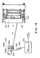
- FIG 13 shows the essential structure of a laser beam scanning portion of such an apparatus.
- a solid state laser element 202 is turned on or off, with a predetermined timing, by a light emitting signal generator 20 in response to inputted imaging signals.
- the laser beam emitted from the solid state laser element 202 travels through a collimator 203, is reflected by a polygon mirror rotating in the direction indicated by an arrow b, and is focused by f- ⁇ lenses 205a, 205b and 205c on the surface of an image bearing member 3, as a spot.
- an exposure distribution which is equivalent to a single image scanning line is formed on the image bearing member surface.
- This scanning cycle is repeated while the image bearing member is rotated by a predetermined peripheral distance in the direction perpendicular to the aforementioned scanning direction, whereby an latent image is formed on the scanned surface, that is, the photosensitive layer on the image bearing member surface. Thereafter, this latent image may be transferred onto a transfer material by a known means.
- a system incorporating a magnetic brush and two component developing agents is frequently used. This is because the latent dot image formed on the image bearing member can be accurately visualized by increasing the density of the magnetic brush. Further, there are other advantages such that a low voltage power source suffices to transfer the toner image borne on the image bearing member onto the transfer material; transfer current utilization efficiency is high; a lesser amount of ozone is produced; and the like. Therefore, a contact type transfer brush is frequently used as a member for generating the transfer electric field.
- EP-0,487,046A discloses an image forming apparatus having a charging brush. However this specification does not provide a solution to the problem with which the present invention is concerned.
- an embodiment of the present invention provides an image forming apparatus capable of producing a high quality image.
- irregular spots are eliminated while increasing the resolution.
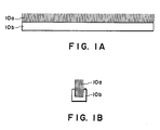
- Figure 1A is a plan view of an embodiment of the transfer brush according to the present invention.
- Figure 1B is a sectional view of the embodiment of the transfer brush according to the present invention.
- Figure 2 is a sectional view of a typical color printer incorporating the electrophotographic system.
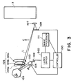
- Figure 3 is a plan view of the exposing member.
- Figure 4 (a) is a graph of the laser driver output.
- Figure 4 (b) is a graph of the output of a solid state laser.
- Figure 5 shows graphs of exposure distribution by the laser.
- Figure 6 is a diagram of a PWM circuit.
- Figure 7 is a timing chart for the PWM circuit operation.
- Figure 8 is an enlarged sectional view of an developing member and its adjacent components.
- Figure 9 is a sectional view of an transferring member and its adjacent components.
- Figure 10 is a perspective view of a transfer drum.
- Figure 11 is a graph showing the relation between the brush density and the half tone image quality when the resolution is 400 dpi.
- Figure 12 is a graph showing the relation between the brush density and the half tone image quality when the resolution is 800 dpi.
- Figure 13 is a schematic view of a laser beam scanning portion.
- Figure 14 is a sectional view of an alternative embodiment of the image forming apparatus in accordance with the present invention.
- Figure 15A is a plan view of an embodiment of the transfer brush in accordance with the present invention.
- Figure 15B is a sectional view of the embodiment of the transfer brush in accordance with the present invention.
- FIG. 2 shows a typical color printer, as an example of image forming apparatus, incorporating the electrophotographic system, in which a transfer brush is employed.
- This printer comprises, as the image bearing member, an electrophotographically sensitive drum 3 which rotates in the direction indicated by an arrow.
- This photosensitive drum 3 is surrounded by a charger 4, a rotational developing apparatus 1 comprising developers 1M, 1C, 1Y and 1BK, a transferring charger 10, a cleaning means 12, and an image forming means comprising a laser beam scanner or the like, and being disposed in the upward direction in the drawing.
- the photosensitive drum 3 is uniformly charged by the charger 4. Then, the charged surface is exposed to a laser beam E modulated by the magenta imaging signals, whereby an electrostatic latent image is formed on the photosensitive drum 3. This latent image is developed by the magenta developer 1M positioned in advance at a predetermined location in the developing station.
- a transfer material advanced by a feed guide 5a, a feed roller 6, and a feed guide 5b is gripped by a gripper 7 of a transfer drum 9, in synchronization with a predetermined timing, and as the transfer drum 9 rotates, the transfer material is wrapped around the transfer drum 9 while being electrostatically adhered to the transfer drum 9 by a contact roller 8 and an electrode which coordinates with the contact roller 8.
- the transfer drum 9 is rotated in the direction indicated by an arrow D, in synchronization with the photosensitive drum, and the visual image which is developed from the aforementioned latent image by the magenta developer 1M is transferred onto the transfer material by the transfer charger 10, in the transfer station.
- the transfer drum 9 continues its rotation to be prepared for transferring the image having next color (cyan in Figure 2).
- the photosensitive drum 3 is cleared of the charge by the charger 11, is cleaned by the cleaning means 12, and then, is charged by the charger 4 to be exposed, in the same manner as the preceding exposure, to a laser beam modulated this time by the cyan imaging signals.
- the developing apparatus 1 is rotated in advance so that the cyan developer 1C is positioned at the predetermined developing location, in the developing station, whereby the toner image of cyan color is formed.
- the transfer material is cleared of charge by a pair of chargers 13 and 14, is released from the aforementioned gripper 7, and then, is separated from the transfer drum 9 by a separating claw 15.
- the transfer material is sent by a conveyer belt 16 to a fixing apparatus (fixing apparatus of a heat roller type), where the toner images are fixed to the transfer material, producing a desired full-color print, which concludes a cycle of the full-color printing sequence.
- the aforementioned laser beam scanner which constitutes an exposing means comprises a semiconductor laser 102, a polygon mirror 105 which revolves at a high speed, and a f- ⁇ lens 106.
- the semiconductor laser 102 serially receives the digital image signals outputted by a computing device, such as a computer, of an image reading (scanning) apparatus, and emits an oscillating laser beam modulated in pulse width in response to the received serial digital imaging signals, to exposes the surface of the photosensitive drum 3.
- the solid state laser element 102 that is, the laser beam source
- a laser driver 500 that is, a generator of light emitting signals, whereby it oscillates the laser beam in response to the beam emitting signals generated by the laser driver.
- the laser beam flux emitted from the solid state laser element 102 is substantially collimated by a collimator lens system 103.
- This collimator lens system 103 is movable by a predetermined distance in the direction indicated by an arrow A, that is, the direction parallel to the beam passage.
- the polygon mirror that is, the rotational multifaceted mirror 105, rotates in the direction indicated by an arrow B at a predetermined constant speed, whereby the collimated beam coming out of the collimator lens system 103 is reflected in such a manner as to be scanned in the predetermined direction, that is, the direction indicated by an arrow C.
- the laser beam flux L is also reflected by a reflective mirror 107 toward a CCD 108 (solid state imaging element) which is a detecting means.
- the CCD 108 comprises a number of optical sensors, which are arranged in such a manner that their arrangement becomes substantially equivalent to the surface arrangement of the photosensitive drum, with reference to the light source.
- the CCD 108 is connected to a controller 100 for controlling the laser driver 500 and a focal point adjusting means 104.
- an image processor 111 is connected to the laser driver 500 and the controller 100.
- an image output signal P is inputted from the image processor 111 to the controller 100, and then, an image signal S is inputted to the laser driver 500, whereby the solid state laser element 102 is caused to oscillate a laser beam with a predetermined timing.
- the laser beam emitted from the solid state laser element 102 is collimated by the collimator lens system 103, becoming a substantially parallel beam, which is made to scan in the arrow C direction, by the rotational polygon mirror 105 rotating in the arrow B direction, and then, is focused by the f- ⁇ lens group 106 onto the photosensitive drum 3 as a spot.
- the laser beam flux L scans across the surface of the photosensitive drum in the above mentioned manner, an exposure distribution equivalent to a single line of scanning is formed on the surface of the photosensitive drum, wherein the photosensitive drum 3 is rotated by a predetermined distance for every scanning.
- a latent image is formed on the photosensitive drum 3, which is equivalent to the exposure distribution formed in response to the image signal S.
- this latent image is recorded as a visual image on a transfer material, through a known electrophotographic process.
- the aforementioned image output signal P is outputted from the image processor 111 before the image signal S is outputted, and it is turned off after the image signal S is turned off.
- the controller 100 ceases its operation while receiving the image output signal P from the image process 111. Therefore, the size and contrast of the picture element can be kept constant during the image forming operation.
- an operational signal from the controller is inputted to the laser driver 500.
- the laser driver generates rectangular waves which oscillate at a constant frequency as shown in Figure 4(a) for a predetermined period, whereby the solid state laser element 102 is turned on and off in response to this signal, oscillating the laser beam it emits.
- the laser beam emitted from the solid state laser element 102 is caused to scan as described above, is reflected by the reflective mirror 107, and is projected onto the CCD 108 positioned at a location which is optically equivalent to the photosensitive drum, scanning thereby the CCD 108.
- the controller 100 resets the accumulated charge of each picture element before the laser beam flux L scans the CCD 108. Each time the CCD 108 is scanned by the spot of laser beams flux, a charge is accumulated in each picture element of the CCD 108, and this accumulated charge is read as an electric signal.
- the CCD 108 is positioned in a manner optically equivalent to the photosensitive drum 8, with respect to the scanning laser beam, and therefore, each time the oscillating laser beam from the solid state laser element 102 scans the CCD 108, the exposure distribution on the surface of the CCD 108 is an intensity distribution pattern correspondent to the spot diameter of the laser beam flux L, as shown in Figure 5. Therefore, the output of each picture element of the CCD 108 displays a distribution shown in Figure 4(b), and this output is sent out as a signal to the controller 100.
- Figure 6 is a diagram of a PWM circuit
- Figure 7 is a timing chart for the PWM circuit operation.
- the PWM circuit comprises a TTL latching circuit for locating the eight bit image signal, a level converter 402 for converting the TTL logic level to the high speed ECL logic level, an ECLD/A converter 403, an ECL comparator 404 for generating the PWM signal, a level converter 405 for converting the ECL logic level to the TTL logic level, a clock generator 406 for generating a clock signal 2f having a frequency twice a picture element clock signal f, a triangular wave generator 407 for generating a substantially idealistic triangular wave signal in synchronization with the clock signal 2f, and a frequency divider 408 for halving the clock signal 2f.
- the ECL logic circuits are installed wherever appropriate.
- a pattern (a) depicts the clock signal 2f
- a pattern (b) depicts the picture element clock signal f having a period twice the signal (a). As is evident from the drawing, they are correlated to the picture element number.
- the triangular wave depicted by a pattern (c) is generated by dividing the clock signal 2f into halves. Further, this triangular wave pattern (c) is converted to the ECL level (0 - -1 V), becoming the triangular wave depicted by a pattern (d).
- a pattern (e) shows several ECL voltage levels obtained by D/A conversion of the image signals, wherein for example, a level correspondent to the first picture element is equivalent to FFH, that is, the black in the gradation level; a level correspondent to the second picture element, to 80H, that is, an intermediate gradation level; a level correspondent to the third picture element, to 40H, that is, another intermediate gradation level; and a level correspondent to the fourth picture element is equivalent to 20H, that is, yet another intermediate gradation level.
- the comparator 404 combines the triangular wave pattern (d) and the image signal pattern (e) to generate PWM signals T, t 2 , t 3 and t 4 which are correspondent to the density of the picture element to be formed. Then, the PWM signal is converted to the TTL level of 0 V or 5 V, becoming the PWM signal depicted by a pattern (f), and is inputted to the laser drive circuit 500.
- an unshown look-up table is provided in front of the latching circuit 401.
- This look-up table is used to execute the ⁇ correction on the image data. It comprise memories storing the ⁇ -corrected data, which are accessed using the eight bit image signal as the address data, to output an image signal carrying ⁇ -corrected data.
- one specific ⁇ -correction table is used for each page of imaging surface, but two or more ⁇ -correction tables may be employed to be switched as needed during the single page of image forming operation. For example, three different tables may be alternately used each time the scanning line is shifted to the next line, in other words, the gradation in the secondary scanning direction is corrected by switching the ⁇ -correction for each scanning line.
- the look-up table may be provided for each of the color toners, for example, yellow, magenta, cyan and black, so that the correction is not affected by the density peculiar to a specific color toner.
- a toner having a low density is matched with a so-called "enhancing" ⁇ -correction table, and a toner having a high density is matched with a ⁇ -correction table having the opposite characteristic.
- a non-linear color masking circuit for example, a secondary color masking circuit, may be provided in the beginning portion of the look-up table.
- the aforementioned PWM system is characterized in that the intermediate tone can be realized by gradating the area size of a dot for each picture element, and therefore, the picture element density does not need to be sacrificed.
- Figure 8 is an enlarged sectional view of one of the developer and its adjacent area in a revolving developing apparatus 1 incorporated in the laser beam printer shown in Figure 1. This developer is located in a developing station, facing the photosensitive drum 3.
- the developer comprises a developing sleeve 22 positioned next to the photosensitive drum 3.
- the developing sleeve 22 is made of non-magnetic material such as aluminum or SUS 316, and is placed in a developing case 36, across an elongated opening formed in the lower left portion of the wall of the developer case, extending in the horizontal direction of the case, wherein an approximately half of its peripheral surface is exposed from the opening, and the rest is in the case. It is supported by bearings and is rotated in the direction indicated by an arrow b.
- a permanent magnet 23 is fixed as a means for generating a fixed magnetic field, holding an attitude as shown in the drawing.
- the magnet 23 has four magnetic poles: magnetic poles 23a (N pole), 23b (S pole), 23c (N), and 23d (S).
- the magnet 23, which is a permanent magnet, may be replaced by an electro-magnet.
- the developer also comprises a non-magnetic blade 24 which serves as a member for regulating the developing agent. It is disposed at the upper lip of the aforementioned opening, through which the developing agent is fed. Its base end is fixed to the developer case wall, and the tip of the other end projects beyond the upper lip of the opening, extending horizontally across the opening.
- This blade 24 is made by bending a piece of SUS 316 in a manner so as for its cross section to form an "L" shape.
- the developer further comprises a magnetic particle regulating member 26, the bottom surface of which serves as a developing agent guiding surface, and this developing agent guiding surface extends to contact the inner surface of the non-magnetic blade 24, at the opening.
- the blade 24, magnetic particle regulating member 26, and the other serve as a regulating members as a whole.
- the developing agent contains magnetic particle 27 and non-magnetic toner 37.
- an elastic sealing member 40 is provided in order to seal the toner which might build up at the bottom of the developer case 36.
- One end of the sealing member 40 is fixed on the case and the other is bent in the rotating direction of the sleeve 22, pressing on the surface of the sleeve 22, so that the developing agent is let in through the contact area between the sealing member 40 and sleeve 22, from the downstream side, with reference to the direction in which the sleeve 22 rotates.
- a plate electrode 30 and a toner feeding roller 60 are provided.
- the plate electrode 30 is imparted with a voltage of the same polarity as the toner, so that the loose toner, that is, the toner which becomes loose during the developing process, is adhered to the photosensitive drum.
- the toner feeding roller 60 is activated in response to the output from the toner density sensor (unshown).
- a piezoelectric element, an inductance sensing element, or the like may be used together with a system in which the developing agent volume is detected, an antenna system in which an alternating bias is utilized, and a system in which the optical density is detected.
- the non-magnetic toner 37 is fed by stopping the rotation of the feed roller 60.
- the fresh developing agent that is, the developing agent replenished with the non-magnetic toner 37, is stirred and mixed while being conveyed by a screw 61. During this conveyance, the replenished toner is triboelectrically charged.
- a divider plate 63 is cut out at each end in the longitudinal direction of the developer, and the fresh developing agent conveyed by the screw 61 is transferred to a screw 62, through these cutouts.
- the S pole 23(d) is a conveyer pole. It recovers the residual developer into the developer case after the development, and conveys the developing agent within the case to the regulating members. In the proximity of the S pole 23(d), the developing agent recovered after the development is exchanged with the fresh developing agent being conveyed by the screw 62 disposed close to the sleeve 22.
- the conveyer screw 64 is provided for equalizing the distribution of the developing agent in the direction of the developing sleeve axis. As the sleeve rotates, the developing agent rides on the sleeve surface and is conveyed toward the screw 64, where it is conveyed in the sleeve axis direction, creating a heap of developing agent moving in the sleeve axis direction. A portion of this heap of developing agent moving in the sleeve axis direction. A portion of this keep of developing agent is pushed back in the direction opposite to the one in which the developing agent on the sleeve is conveyed, within a space M shown in Figure 8.
- the screw 64 delivers the developing agent in the direction opposite to the one in which the screw 6 does.
- Such a developer structure is effective also in the case in which a mixture of the magnetic particle and the non-magnetic toner, or the magnetic particle and a slightly magnetic toner, is in the developing agent container.
- the distance d 2 between the tip of the non-magnetic blade 24 and the developing sleeve 22 is 50 - 900 ⁇ m, preferably 150 - 800 ⁇ m. If this distance is no more than 50 ⁇ m, the gap is clogged with the magnetic particle, causing thereby the developing agent to be distributed as an uneven layer. This makes it impossible to coat the developing agent on the surface of the sleeve, in such a manner that the image is properly developed, resulting n an image having a low density and irregular tone reproduction.
- magnetic particles in this magnetic particle layer are carried on the sleeve 22 and conveyed in the arrow b direction in which the sleeve 22 is rotated, the farther their distances from the surface of the sleeve 22 are, the slower the speed at which they move as the sleeve 22 is rotated are, because of the balance between the magnetic force, effect of gravity, and force urging it to move in the rotating direction of the sleeve 22. Of course, some of them fall of the sleeve 22 because of the effect of gravity.
- the magnetic particles create a dynamic layer in which the closer the magnetic particles are to the surface of the sleeve 22, the more they shift toward the magnetic pole 23a.
- the magnetic particles and the toner are supplied to the developing station where they develop the image.
- Figure 1 shows an example of the transfer brush incorporated in an embodiment of the image forming apparatus in accordance with the present invention.
- Figure 1A is a plan view
- Figure 1B is a sectional view
- a conductive brush 10a is composed of micro-acrylic fiber which is made conductive by being dyed with copper sulfate.
- this conductive fiber may be replaced with conductive or semi-conductive material: stainless steel fiber measuring 8 - 15 ⁇ m in cross sectional area size; resin fiber, such as acrylic fiber, nylon fiber, polyester fiber, rayon fiber, or the like, which is plated with metal; composite material in which conductive material such as carbon or metallic powder is mixed in resin; carbon fiber composed by carbonizing the resin fiber or the like, to impart conductivity; or the like.
- volume resistivity material having a volume resistivity value of no more than 10 10 ⁇ /cm, preferably no more than 10 8 , is usable.
- Figure 9 shows a sectional view of the transferring member.
- the conductive fiber brush 10 is pressed on a dielectric material sheet 93 because of the elasticity of an elastic dielectric material sheet 10c, such as 125 ⁇ m thick polyethylene telephthalate (PET) or the like, which covers one side of the conductive fiber brush 10.
- the conductive fiber brush 10 is connected to a transfer power source 40.
- a transfer electric field generating means having such a structure as described above induces no such current that does not directly contribute to the transfer operation, as the current which flows to the shield if the corona discharger is employed, and therefore, all of the current flowing from the transfer power source contributes as the transfer charge current.
- FIG 10 is a perspective view of a transfer drum.
- a transfer drum 9 comprises a pair of cylinders 9a and 9b made of conductive material such as metal, a connecting member 9c which connects the cylinders 9a and 9b, and transfer material carrying member, that is, the dielectric material sheet 93, which is spread between the cylinders 9a and 9b in a manner to complete the transfer drum 9.
- the dielectric material sheet 93 must satisfy at least two of the conditions: that the dielectric constant is 3.0 - 13.0; that the volume resistivity is 10 9 - 10 14 ⁇ /cm; and that the thickness is 70 - 200 ⁇ m, and is composed of, for example, polyfluorovinylidene resin (PVdF) film.
- PVdF polyfluorovinylidene resin
- the diameter of the transfer drum 9 is 160 mm, and its rotating speed is set at 160 mm/sec. Also, he process speed, that is, the moving speed of the photosensitive drum 3 or the like, is set at 160 mm/sec.
- the toner employed in this embodiment is composed of colored resin particles (containing bonding resin and coloring agent, as well as other additives if necessary) containing filler such as micro-particles of hydrophobic colloidal silica. More particularly, it is a polyester resin with a negative charge polarity, and its volume average particle diameter is 8 ⁇ m.
- latent halftone dot images having a resolution of 400 dpi and 800 dpi, respectively, were formed and developed, they were transferred using the transfer brush while the brush density was varied, and the picture quality of the transferred image samples were evaluated. As a result, it became evident that if the density of the transfer brush was not high, a tone reproduction irregularity developed.
- Figure 11 shows the relation between the brush density and the picture quality when the latent halftone dot image having 400 dip (15.7 dot/mm) was formed.
- the picture quality was rated using the subjective evaluations consisting of five grades:
- Figure 12 shows the relation between the brush density and the picture quality when the latent half tone dot image having a density of 800 dpi (31.5 dot/mm) was formed.
- the produced image was evaluated in the same manner as the above described case in which the dot density was 400 dpi.
- Figure 14 is an alternative embodiment of the image forming apparatus in accordance with the present invention.
- the image forming apparatus is a full color laser beam printer, whereas it is different from the one used in the preceding embodiment, in that a dedicated image bearing member is provided for each color.
- this embodiment comprises dedicated photosensitive drums 3Y (yellow), 3M (magenta), 3C (cyan), and 3BK (black), which are surrounded, respectively, by: dedicated laser beam scanners 80Y, 80M, 80C, and 80BK; dedicated developers 1Y, 1M, 1C and 1BK; dedicated transfer dischargers 10Y, 10M, 10C and 10BK; and dedicated cleaners 12Y, 12M, 12C and 12BK.
- the transfer material is fed through a feed guide 5a, and is delivered through a feed roller 6 and a guide 5b. Then, it is subjected to the corona discharge from the adhesion charger 81, whereby it is securely adhered onto the conveyer belt 9a.
- the images formed on respective photosensitive drums are transferred by the brushes 10Y, 10M, 10C and 10BK onto the transfer material.
- the transfer material is cleared of the charge by the charge removing member 82, whereby it is separated from the conveyer belt 9a.
- the images are fixed onto the recording material by a fixing member 17, offering thereby a full-color image.
- conductive brushes 10Y, 10M, 10C and 10BK that is, the means for generating the electric field, are in contact with the inner side surface of the transfer belt 9a, that is, the transfer material carrying member. Further, an unshown bias voltage power source which generates the transfer electric field is connected to the conductive brush 10Y, 10M, 10C and 10BK.
- the conductive brush diagonally extends from the entrance side of the transfer material toward the downstream side of the transfer belt 9a, and because of its elasticity and its extreme proximity to the transfer belt 9a, it presses itself upon the transfer belt 9a across a range between where the transfer material being carried on the transfer belt 9a begins its contact with the photosensitive drum and where it begins to lose its contact.
- a sheet of different type of dielectric material, or a compound sheet made of various types of dielectric material my be used for the transfer belt 9a.
- a sheet of 150 ⁇ m thick polyfluorovinylidene (PVdF) was used.
- This embodiment was subjected to a text in which a latent halftone dot image having a resolution of 400 dpi, or 800 dip, was formed, and then, the latent image was developed in reversal into a visible image, using a toner having an approximate average diameter of 8 ⁇ m.
- the image samples were evaluated in the same manner as the test of the preceding embodiment, in which the transfer brush density was varied. An excellent images was obtained when the brush density was twice or more the resolution of the latent dot image.
- Figure 15 shows an example of a brush in which a large number of bristles are compacted in order to increase the transfer brush density
- Figure 15A is a plan view
- Figure 15B is a sectional view in which the bundle of bristles are placed in two layers in the brush.
- the image forming means according to the present invention which is structured in the aforementioned manner can form a high quality picture image in which tone reproduction is excellent even in the area where the image density is low, in other words, there is no tone reproduction irregularity.
- tone reproduction irregularity in the highlight and halftone areas becomes more conspicuous as the resolution is increased, an excellent picture image can be nonetheless produced if a transfer brush having a density twice or more the resolution of the latent dot image is used or the transfer operation after the latent dot image is formed and developed.
Landscapes
- Physics & Mathematics (AREA)
- General Physics & Mathematics (AREA)
- Electrostatic Charge, Transfer And Separation In Electrography (AREA)
- Color Electrophotography (AREA)
- Control Or Security For Electrophotography (AREA)
Description
- The present invention relates to an image forming apparatus, such as an electrostatic copying machine or printer, which incorporates an electrostatic transferring process.
- A process in which a latent image is formed in response to analog signals has been widely used in a copying machine or the like. In particular, a process in which a latent dot image is formed on an image bearing member by turning on or off a laser beam has come to be widely used in an image forming apparatus to be used for color image formation which requires stricter image forming conditions.
- When this type of apparatus is used to form an image, a binary recording system is satisfactory if an original contains only an image such as text or the like, but it is not satisfactory if the original contains an image such as a photograph or the like. This is because a half tone must be reproduced in the case of latter. Therefore, imaging systems such as the design system, density pattern system, and the like have been proposed as a method capable of reproducing the half tone while using the binary recording system.
- However, since this type of recording means involves the problem that high resolution is difficult to achieve, a recording means has been devised in order to provide a solution. In this recording means, the dot size is varied in each picture element by PW (pulse-width)-modulating the laser beam, whereby the tone reproduction is accomplished without reducing the picture element density. In other words, an excellent halftone image can be obtained without sacrificing the high resolution. Such a recording means is desirable in the case of the color image forming apparatus which requires strict image forming conditions.
- Figure 13 shows the essential structure of a laser beam scanning portion of such an apparatus. To describe briefly this portion, a solid
state laser element 202 is turned on or off, with a predetermined timing, by a lightemitting signal generator 20 in response to inputted imaging signals. The laser beam emitted from the solidstate laser element 202 travels through acollimator 203, is reflected by a polygon mirror rotating in the direction indicated by an arrow b, and is focused by f-θ lenses image bearing member 3, as a spot. - Thus, an exposure distribution which is equivalent to a single image scanning line is formed on the image bearing member surface. This scanning cycle is repeated while the image bearing member is rotated by a predetermined peripheral distance in the direction perpendicular to the aforementioned scanning direction, whereby an latent image is formed on the scanned surface, that is, the photosensitive layer on the image bearing member surface. Thereafter, this latent image may be transferred onto a transfer material by a known means.
- In image formation, in particular, the image formation using a high resolution color image forming apparatus, a system incorporating a magnetic brush and two component developing agents is frequently used. This is because the latent dot image formed on the image bearing member can be accurately visualized by increasing the density of the magnetic brush. Further, there are other advantages such that a low voltage power source suffices to transfer the toner image borne on the image bearing member onto the transfer material; transfer current utilization efficiency is high; a lesser amount of ozone is produced; and the like. Therefore, a contact type transfer brush is frequently used as a member for generating the transfer electric field.
- However, when a prior image forming means as described above is used, irregular spots are sometimes generated during the transfer operation even after the latent dot image is accurately developed. Such imaging faults occur with the use of not only the binary recording system but also the PWM system. In particular, they are likely to occur in the highlight portion. This phenomenon becomes more noticeable when the latent dot image resolution is increased.
- European Patent Specification No. EP-0,487,046A discloses an image forming apparatus having a charging brush. However this specification does not provide a solution to the problem with which the present invention is concerned.
- In accordance with the present invention there is provided an image forming apparatus as set out in
claim 1. - Thus an embodiment of the present invention provides an image forming apparatus capable of producing a high quality image.
- According to an aspect of the present invention, irregular spots are eliminated while increasing the resolution.
- These and other features of the invention will be more readily understood upon a consideration of the following exemplary description of preferred embodiments of the present invention taken in conjunction with the accompanying drawings, in which:
- Figure 1A is a plan view of an embodiment of the transfer brush according to the present invention.
- Figure 1B is a sectional view of the embodiment of the transfer brush according to the present invention.
- Figure 2 is a sectional view of a typical color printer incorporating the electrophotographic system.
- Figure 3 is a plan view of the exposing member.
- Figure 4, (a) is a graph of the laser driver output. Figure 4, (b) is a graph of the output of a solid state laser.
- Figure 5 shows graphs of exposure distribution by the laser.
- Figure 6 is a diagram of a PWM circuit.
- Figure 7 is a timing chart for the PWM circuit operation.
- Figure 8 is an enlarged sectional view of an developing member and its adjacent components.
- Figure 9 is a sectional view of an transferring member and its adjacent components.
- Figure 10 is a perspective view of a transfer drum.
- Figure 11 is a graph showing the relation between the brush density and the half tone image quality when the resolution is 400 dpi.
- Figure 12 is a graph showing the relation between the brush density and the half tone image quality when the resolution is 800 dpi.
- Figure 13 is a schematic view of a laser beam scanning portion.
- Figure 14 is a sectional view of an alternative embodiment of the image forming apparatus in accordance with the present invention.
- Figure 15A is a plan view of an embodiment of the transfer brush in accordance with the present invention. Figure 15B is a sectional view of the embodiment of the transfer brush in accordance with the present invention.
- Figure 2 shows a typical color printer, as an example of image forming apparatus, incorporating the electrophotographic system, in which a transfer brush is employed. This printer comprises, as the image bearing member, an electrophotographically
sensitive drum 3 which rotates in the direction indicated by an arrow. Thisphotosensitive drum 3 is surrounded by a charger 4, a rotational developingapparatus 1 comprisingdevelopers charger 10, acleaning means 12, and an image forming means comprising a laser beam scanner or the like, and being disposed in the upward direction in the drawing. - Next, the overall operational sequence of the color printer is briefly described, referring to the full-color mode. The
photosensitive drum 3 is uniformly charged by the charger 4. Then, the charged surface is exposed to a laser beam E modulated by the magenta imaging signals, whereby an electrostatic latent image is formed on thephotosensitive drum 3. This latent image is developed by the magentadeveloper 1M positioned in advance at a predetermined location in the developing station. - Meanwhile, a transfer material advanced by a
feed guide 5a, afeed roller 6, and afeed guide 5b is gripped by agripper 7 of atransfer drum 9, in synchronization with a predetermined timing, and as thetransfer drum 9 rotates, the transfer material is wrapped around thetransfer drum 9 while being electrostatically adhered to thetransfer drum 9 by acontact roller 8 and an electrode which coordinates with thecontact roller 8. Thetransfer drum 9 is rotated in the direction indicated by an arrow D, in synchronization with the photosensitive drum, and the visual image which is developed from the aforementioned latent image by themagenta developer 1M is transferred onto the transfer material by thetransfer charger 10, in the transfer station. Thetransfer drum 9 continues its rotation to be prepared for transferring the image having next color (cyan in Figure 2). - On the other hand, the
photosensitive drum 3 is cleared of the charge by the charger 11, is cleaned by thecleaning means 12, and then, is charged by the charger 4 to be exposed, in the same manner as the preceding exposure, to a laser beam modulated this time by the cyan imaging signals. Meanwhile, the developingapparatus 1 is rotated in advance so that thecyan developer 1C is positioned at the predetermined developing location, in the developing station, whereby the toner image of cyan color is formed. - The same image forming process is repeated for yellow and black colors. After four toner images of different color are transferred onto the transfer material, the transfer material is cleared of charge by a pair of
chargers aforementioned gripper 7, and then, is separated from thetransfer drum 9 by a separatingclaw 15. Next, the transfer material is sent by aconveyer belt 16 to a fixing apparatus (fixing apparatus of a heat roller type), where the toner images are fixed to the transfer material, producing a desired full-color print, which concludes a cycle of the full-color printing sequence. - Referring to Figure 3, the aforementioned laser beam scanner which constitutes an exposing means comprises a
semiconductor laser 102, apolygon mirror 105 which revolves at a high speed, and a f-θ lens 106. Thesemiconductor laser 102 serially receives the digital image signals outputted by a computing device, such as a computer, of an image reading (scanning) apparatus, and emits an oscillating laser beam modulated in pulse width in response to the received serial digital imaging signals, to exposes the surface of thephotosensitive drum 3. - More particularly, referring to Figure 3, the solid
state laser element 102, that is, the laser beam source, is connected to alaser driver 500, that is, a generator of light emitting signals, whereby it oscillates the laser beam in response to the beam emitting signals generated by the laser driver. The laser beam flux emitted from the solidstate laser element 102 is substantially collimated by acollimator lens system 103. Thiscollimator lens system 103 is movable by a predetermined distance in the direction indicated by an arrow A, that is, the direction parallel to the beam passage. - The polygon mirror, that is, the rotational
multifaceted mirror 105, rotates in the direction indicated by an arrow B at a predetermined constant speed, whereby the collimated beam coming out of thecollimator lens system 103 is reflected in such a manner as to be scanned in the predetermined direction, that is, the direction indicated by an arrow C. The f-θ lens group 106 (10a, 106b, 106c) disposed on the downstream side of the beam passage, with reference to therotational polygon mirror 105, focuses the laser beam flux polarized by the polygon mirror on the surface to be scanned, that is, on thephotosensitive drum 8, as a spot which scans the surface to be scanned, at a constant scanning speed. - While scanning the surface of the
photosensitive drum 3 which is the surface to be scanned, the laser beam flux L is also reflected by areflective mirror 107 toward a CCD 108 (solid state imaging element) which is a detecting means. TheCCD 108 comprises a number of optical sensors, which are arranged in such a manner that their arrangement becomes substantially equivalent to the surface arrangement of the photosensitive drum, with reference to the light source. Also, theCCD 108 is connected to acontroller 100 for controlling thelaser driver 500 and a focal point adjusting means 104. Further, an image processor 111 is connected to thelaser driver 500 and thecontroller 100. - As for the operational sequence for forming a desired image using an apparatus with the above-described structure, first, an image output signal P is inputted from the image processor 111 to the
controller 100, and then, an image signal S is inputted to thelaser driver 500, whereby the solidstate laser element 102 is caused to oscillate a laser beam with a predetermined timing. - The laser beam emitted from the solid
state laser element 102 is collimated by thecollimator lens system 103, becoming a substantially parallel beam, which is made to scan in the arrow C direction, by therotational polygon mirror 105 rotating in the arrow B direction, and then, is focused by the f-θ lens group 106 onto thephotosensitive drum 3 as a spot. Each time the laser beam flux L scans across the surface of the photosensitive drum in the above mentioned manner, an exposure distribution equivalent to a single line of scanning is formed on the surface of the photosensitive drum, wherein thephotosensitive drum 3 is rotated by a predetermined distance for every scanning. As a result, a latent image is formed on thephotosensitive drum 3, which is equivalent to the exposure distribution formed in response to the image signal S. Then, this latent image is recorded as a visual image on a transfer material, through a known electrophotographic process. - The aforementioned image output signal P is outputted from the image processor 111 before the image signal S is outputted, and it is turned off after the image signal S is turned off. The
controller 100 ceases its operation while receiving the image output signal P from the image process 111. Therefore, the size and contrast of the picture element can be kept constant during the image forming operation. - Next, the operation of the laser beam flux focal point adjusting means 104 is described.
- First, an operational signal from the controller is inputted to the
laser driver 500. The laser driver generates rectangular waves which oscillate at a constant frequency as shown in Figure 4(a) for a predetermined period, whereby the solidstate laser element 102 is turned on and off in response to this signal, oscillating the laser beam it emits. The laser beam emitted from the solidstate laser element 102 is caused to scan as described above, is reflected by thereflective mirror 107, and is projected onto theCCD 108 positioned at a location which is optically equivalent to the photosensitive drum, scanning thereby theCCD 108. - The
controller 100 resets the accumulated charge of each picture element before the laser beam flux L scans theCCD 108. Each time theCCD 108 is scanned by the spot of laser beams flux, a charge is accumulated in each picture element of theCCD 108, and this accumulated charge is read as an electric signal. - The
CCD 108 is positioned in a manner optically equivalent to thephotosensitive drum 8, with respect to the scanning laser beam, and therefore, each time the oscillating laser beam from the solidstate laser element 102 scans theCCD 108, the exposure distribution on the surface of theCCD 108 is an intensity distribution pattern correspondent to the spot diameter of the laser beam flux L, as shown in Figure 5. Therefore, the output of each picture element of theCCD 108 displays a distribution shown in Figure 4(b), and this output is sent out as a signal to thecontroller 100. Thecontroller 100 computes a contrast V with use of the following formula, wherein the maximum value of the output of theCCD 108 is θmax, and the minimum value is θmin.
- In this case, the smaller the spot diameter is, the higher the contrast V is, and therefore, when a value of the V computed from the formula (1) is not equal to a predetermined value V0, a driving signal is sent from the
controller 100 to the focusing means 104, to move thecollimator lens system 103 in the arrow A direction by a predetermined distance. Then, the V is measured again, with thecollimator lens system 103 being at a new location, to compare the new value of the V with V0. Eventually, thecollimator lens system 103 is fixed at a location where the measured value of V becomes equal to V0, thereby the focusing error of the optical system is corrected, realizing thereby the smallest diameter for the scanning spot of the laser beam flux L. - Figure 6 is a diagram of a PWM circuit, and Figure 7 is a timing chart for the PWM circuit operation.
- Referring to Figure 6, the PWM circuit comprises a TTL latching circuit for locating the eight bit image signal, a
level converter 402 for converting the TTL logic level to the high speed ECL logic level, an ECLD/A converter 403, anECL comparator 404 for generating the PWM signal, alevel converter 405 for converting the ECL logic level to the TTL logic level, aclock generator 406 for generating aclock signal 2f having a frequency twice a picture element clock signal f, atriangular wave generator 407 for generating a substantially idealistic triangular wave signal in synchronization with theclock signal 2f, and afrequency divider 408 for halving theclock signal 2f. Further, in order to allow the circuit to operate at a high speed, the ECL logic circuits are installed wherever appropriate. - The circuit having such a structure is described referring to Figure 7.
- A pattern (a) depicts the
clock signal 2f, and a pattern (b) depicts the picture element clock signal f having a period twice the signal (a). As is evident from the drawing, they are correlated to the picture element number. Also in thetriangular wave generator 407, in order to hold the duty ratio of the triangular wave signal at 50 % level, the triangular wave depicted by a pattern (c) is generated by dividing theclock signal 2f into halves. Further, this triangular wave pattern (c) is converted to the ECL level (0 - -1 V), becoming the triangular wave depicted by a pattern (d). - On the other hand, the image signal intensity fluctuates within a gradation range from OOH (white) to FFH (black), constituting thereby 256 gradation levels, wherein the code H stands for the hexadecimal code. A pattern (e) shows several ECL voltage levels obtained by D/A conversion of the image signals, wherein for example, a level correspondent to the first picture element is equivalent to FFH, that is, the black in the gradation level; a level correspondent to the second picture element, to 80H, that is, an intermediate gradation level; a level correspondent to the third picture element, to 40H, that is, another intermediate gradation level; and a level correspondent to the fourth picture element is equivalent to 20H, that is, yet another intermediate gradation level. The
comparator 404 combines the triangular wave pattern (d) and the image signal pattern (e) to generate PWM signals T, t2, t3 and t4 which are correspondent to the density of the picture element to be formed. Then, the PWM signal is converted to the TTL level of 0 V or 5 V, becoming the PWM signal depicted by a pattern (f), and is inputted to thelaser drive circuit 500. - In the circuit shown in Figure 6, an unshown look-up table is provided in front of the latching
circuit 401. This look-up table is used to execute the γ correction on the image data. It comprise memories storing the γ-corrected data, which are accessed using the eight bit image signal as the address data, to output an image signal carrying γ-corrected data. Normally, one specific γ-correction table is used for each page of imaging surface, but two or more γ-correction tables may be employed to be switched as needed during the single page of image forming operation. For example, three different tables may be alternately used each time the scanning line is shifted to the next line, in other words, the gradation in the secondary scanning direction is corrected by switching the γ-correction for each scanning line. - Further, the look-up table may be provided for each of the color toners, for example, yellow, magenta, cyan and black, so that the correction is not affected by the density peculiar to a specific color toner. In other words, a toner having a low density is matched with a so-called "enhancing" γ-correction table, and a toner having a high density is matched with a γ-correction table having the opposite characteristic. Also, in order to correct the murkiness of each other color, a non-linear color masking circuit, for example, a secondary color masking circuit, may be provided in the beginning portion of the look-up table.
- The aforementioned PWM system is characterized in that the intermediate tone can be realized by gradating the area size of a dot for each picture element, and therefore, the picture element density does not need to be sacrificed.
- Hereinafter, the present invention will be further described, referring to the embodiments.
- Figure 8 is an enlarged sectional view of one of the developer and its adjacent area in a revolving developing
apparatus 1 incorporated in the laser beam printer shown in Figure 1. This developer is located in a developing station, facing thephotosensitive drum 3. - The developer comprises a developing sleeve 22 positioned next to the
photosensitive drum 3. The developing sleeve 22 is made of non-magnetic material such as aluminum or SUS 316, and is placed in a developing case 36, across an elongated opening formed in the lower left portion of the wall of the developer case, extending in the horizontal direction of the case, wherein an approximately half of its peripheral surface is exposed from the opening, and the rest is in the case. It is supported by bearings and is rotated in the direction indicated by an arrow b. - Within the developing sleeve 22, a
permanent magnet 23 is fixed as a means for generating a fixed magnetic field, holding an attitude as shown in the drawing. Themagnet 23 has four magnetic poles:magnetic poles 23a (N pole), 23b (S pole), 23c (N), and 23d (S). Themagnet 23, which is a permanent magnet, may be replaced by an electro-magnet. - The developer also comprises a
non-magnetic blade 24 which serves as a member for regulating the developing agent. It is disposed at the upper lip of the aforementioned opening, through which the developing agent is fed. Its base end is fixed to the developer case wall, and the tip of the other end projects beyond the upper lip of the opening, extending horizontally across the opening. Thisblade 24 is made by bending a piece of SUS 316 in a manner so as for its cross section to form an "L" shape. - The developer further comprises a magnetic
particle regulating member 26, the bottom surface of which serves as a developing agent guiding surface, and this developing agent guiding surface extends to contact the inner surface of thenon-magnetic blade 24, at the opening. Theblade 24, magneticparticle regulating member 26, and the other serve as a regulating members as a whole. - The developing agent contains magnetic particle 27 and
non-magnetic toner 37. In order to seal the toner which might build up at the bottom of the developer case 36, anelastic sealing member 40 is provided. One end of the sealingmember 40 is fixed on the case and the other is bent in the rotating direction of the sleeve 22, pressing on the surface of the sleeve 22, so that the developing agent is let in through the contact area between the sealingmember 40 and sleeve 22, from the downstream side, with reference to the direction in which the sleeve 22 rotates. - Also in the developer case, a
plate electrode 30 and atoner feeding roller 60 are provided. Theplate electrode 30 is imparted with a voltage of the same polarity as the toner, so that the loose toner, that is, the toner which becomes loose during the developing process, is adhered to the photosensitive drum. Thetoner feeding roller 60 is activated in response to the output from the toner density sensor (unshown). As for sensing means, a piezoelectric element, an inductance sensing element, or the like may be used together with a system in which the developing agent volume is detected, an antenna system in which an alternating bias is utilized, and a system in which the optical density is detected. Thenon-magnetic toner 37 is fed by stopping the rotation of thefeed roller 60. The fresh developing agent, that is, the developing agent replenished with thenon-magnetic toner 37, is stirred and mixed while being conveyed by ascrew 61. During this conveyance, the replenished toner is triboelectrically charged. Adivider plate 63 is cut out at each end in the longitudinal direction of the developer, and the fresh developing agent conveyed by thescrew 61 is transferred to ascrew 62, through these cutouts. - The S pole 23(d) is a conveyer pole. It recovers the residual developer into the developer case after the development, and conveys the developing agent within the case to the regulating members. In the proximity of the S pole 23(d), the developing agent recovered after the development is exchanged with the fresh developing agent being conveyed by the
screw 62 disposed close to the sleeve 22. - The
conveyer screw 64 is provided for equalizing the distribution of the developing agent in the direction of the developing sleeve axis. As the sleeve rotates, the developing agent rides on the sleeve surface and is conveyed toward thescrew 64, where it is conveyed in the sleeve axis direction, creating a heap of developing agent moving in the sleeve axis direction. A portion of this heap of developing agent moving in the sleeve axis direction. A portion of this keep of developing agent is pushed back in the direction opposite to the one in which the developing agent on the sleeve is conveyed, within a space M shown in Figure 8. Thescrew 64 delivers the developing agent in the direction opposite to the one in which thescrew 6 does. - Such a developer structure is effective also in the case in which a mixture of the magnetic particle and the non-magnetic toner, or the magnetic particle and a slightly magnetic toner, is in the developing agent container.
- The distance d2 between the tip of the
non-magnetic blade 24 and the developing sleeve 22 is 50 - 900 µm, preferably 150 - 800 µm. If this distance is no more than 50 µm, the gap is clogged with the magnetic particle, causing thereby the developing agent to be distributed as an uneven layer. This makes it impossible to coat the developing agent on the surface of the sleeve, in such a manner that the image is properly developed, resulting n an image having a low density and irregular tone reproduction. - Though magnetic particles in this magnetic particle layer are carried on the sleeve 22 and conveyed in the arrow b direction in which the sleeve 22 is rotated, the farther their distances from the surface of the sleeve 22 are, the slower the speed at which they move as the sleeve 22 is rotated are, because of the balance between the magnetic force, effect of gravity, and force urging it to move in the rotating direction of the sleeve 22. Of course, some of them fall of the sleeve 22 because of the effect of gravity.
- Therefore, when the
magnetic poles magnetic pole 23a. As the magnetic particles shift while the sleeve 22 is rotated, the magnetic particles and the toner are supplied to the developing station where they develop the image. - Figure 1 shows an example of the transfer brush incorporated in an embodiment of the image forming apparatus in accordance with the present invention.
- Figure 1A is a plan view, and Figure 1B is a sectional view. In this embodiment, a
conductive brush 10a is composed of micro-acrylic fiber which is made conductive by being dyed with copper sulfate. However, this conductive fiber may be replaced with conductive or semi-conductive material: stainless steel fiber measuring 8 - 15 µm in cross sectional area size; resin fiber, such as acrylic fiber, nylon fiber, polyester fiber, rayon fiber, or the like, which is plated with metal; composite material in which conductive material such as carbon or metallic powder is mixed in resin; carbon fiber composed by carbonizing the resin fiber or the like, to impart conductivity; or the like. - As for the volume resistivity, material having a volume resistivity value of no more than 1010 Ω/cm, preferably no more than 108, is usable.
- Figure 9 shows a sectional view of the transferring member.
- The
conductive fiber brush 10 is pressed on adielectric material sheet 93 because of the elasticity of an elastic dielectric material sheet 10c, such as 125 µm thick polyethylene telephthalate (PET) or the like, which covers one side of theconductive fiber brush 10. The other side of theconductive fiber brush 10, which faces the back side of thedielectric material sheet 93 where theconductive fiber brush 10 contacts thedielectric material sheet 93, is covered with an electricfield regulating member 10b composed of a dielectric material sheet such as 50 µm thick PET sheet (polyethylene telephthalate) or the like, so that the electric field is shielded on the upstream side of the transfer station. Theconductive fiber brush 10 is connected to atransfer power source 40. A transfer electric field generating means having such a structure as described above induces no such current that does not directly contribute to the transfer operation, as the current which flows to the shield if the corona discharger is employed, and therefore, all of the current flowing from the transfer power source contributes as the transfer charge current. - Figure 10 is a perspective view of a transfer drum. A
transfer drum 9 comprises a pair ofcylinders member 9c which connects thecylinders dielectric material sheet 93, which is spread between thecylinders transfer drum 9. Thedielectric material sheet 93 must satisfy at least two of the conditions: that the dielectric constant is 3.0 - 13.0; that the volume resistivity is 109 - 1014 Ω/cm; and that the thickness is 70 - 200 µm, and is composed of, for example, polyfluorovinylidene resin (PVdF) film. The leading end and the trailing end of thedielectric material sheet 93 are fixed on the connectingmember 9c. - In this embodiment, the diameter of the
transfer drum 9 is 160 mm, and its rotating speed is set at 160 mm/sec. Also, he process speed, that is, the moving speed of thephotosensitive drum 3 or the like, is set at 160 mm/sec. - The toner employed in this embodiment is composed of colored resin particles (containing bonding resin and coloring agent, as well as other additives if necessary) containing filler such as micro-particles of hydrophobic colloidal silica. More particularly, it is a polyester resin with a negative charge polarity, and its volume average particle diameter is 8 µm.
- After latent halftone dot images having a resolution of 400 dpi and 800 dpi, respectively, were formed and developed, they were transferred using the transfer brush while the brush density was varied, and the picture quality of the transferred image samples were evaluated. As a result, it became evident that if the density of the transfer brush was not high, a tone reproduction irregularity developed.
- Figure 11 shows the relation between the brush density and the picture quality when the latent halftone dot image having 400 dip (15.7 dot/mm) was formed.
- The picture quality was rated using the subjective evaluations consisting of five grades:
- 5 ... Excellent
- 4 ... Good
- 3 ... Average
- 2 ... Bad
- 1 ... Poor
- wherein, 30 evaluators were asked to give subjective points to the produced images, twice for each images, making a total of 60 evaluations, and then, the average value was plotted in the graph. It is evident according to the graph that the picture quality linearly improved as the brush density was increased from five line/mm to 30 line/mm, and when the brush density was higher than 30 line/mm, an excellent image with no tone reproduction irregularity could be obtained.
- Figure 12 shows the relation between the brush density and the picture quality when the latent half tone dot image having a density of 800 dpi (31.5 dot/mm) was formed. The produced image was evaluated in the same manner as the above described case in which the dot density was 400 dpi.
- It is evident from this graph that the picture quality improved as the brush density was increased from the 10 line/mm to 60 line/mm, and when the picture density was more than 60 line/mm, an excellent image with no tone reproduction irregularity could be obtained.
- Figure 14 is an alternative embodiment of the image forming apparatus in accordance with the present invention.
- In this embodiment, the image forming apparatus is a full color laser beam printer, whereas it is different from the one used in the preceding embodiment, in that a dedicated image bearing member is provided for each color. In other words, this embodiment comprises dedicated
photosensitive drums 3Y (yellow), 3M (magenta), 3C (cyan), and 3BK (black), which are surrounded, respectively, by: dedicatedlaser beam scanners dedicated developers dedicated cleaners - The transfer material is fed through a
feed guide 5a, and is delivered through afeed roller 6 and aguide 5b. Then, it is subjected to the corona discharge from theadhesion charger 81, whereby it is securely adhered onto theconveyer belt 9a. - Next, the images formed on respective photosensitive drums are transferred by the brushes 10Y, 10M, 10C and 10BK onto the transfer material. Then, the transfer material is cleared of the charge by the
charge removing member 82, whereby it is separated from theconveyer belt 9a. Then, the images are fixed onto the recording material by a fixingmember 17, offering thereby a full-color image. - In Figure 14, conductive brushes 10Y, 10M, 10C and 10BK, that is, the means for generating the electric field, are in contact with the inner side surface of the
transfer belt 9a, that is, the transfer material carrying member. Further, an unshown bias voltage power source which generates the transfer electric field is connected to the conductive brush 10Y, 10M, 10C and 10BK. - As for the positioning of the conductive brush, the conductive brush diagonally extends from the entrance side of the transfer material toward the downstream side of the
transfer belt 9a, and because of its elasticity and its extreme proximity to thetransfer belt 9a, it presses itself upon thetransfer belt 9a across a range between where the transfer material being carried on thetransfer belt 9a begins its contact with the photosensitive drum and where it begins to lose its contact. As for thetransfer belt 9a, a sheet of different type of dielectric material, or a compound sheet made of various types of dielectric material my be used for thetransfer belt 9a. However, in this embodiment, a sheet of 150 µm thick polyfluorovinylidene (PVdF) was used. This embodiment was subjected to a text in which a latent halftone dot image having a resolution of 400 dpi, or 800 dip, was formed, and then, the latent image was developed in reversal into a visible image, using a toner having an approximate average diameter of 8 µm. The image samples were evaluated in the same manner as the test of the preceding embodiment, in which the transfer brush density was varied. An excellent images was obtained when the brush density was twice or more the resolution of the latent dot image. - Figure 15 shows an example of a brush in which a large number of bristles are compacted in order to increase the transfer brush density, wherein Figure 15A is a plan view, and Figure 15B is a sectional view in which the bundle of bristles are placed in two layers in the brush. When the brush was made as shown in the sectional view, a brush density of approximately 100 line/mm was accomplished, offering an excellent picture image.
- The image forming means according to the present invention which is structured in the aforementioned manner can form a high quality picture image in which tone reproduction is excellent even in the area where the image density is low, in other words, there is no tone reproduction irregularity.
- More specifically, though the tone reproduction irregularity in the highlight and halftone areas becomes more conspicuous as the resolution is increased, an excellent picture image can be nonetheless produced if a transfer brush having a density twice or more the resolution of the latent dot image is used or the transfer operation after the latent dot image is formed and developed.
- While the invention has been described with reference to the structures disclosed herein, it is not confined to the details set forth and this application is intended to cover such modifications or changes as may come within the scope of the following claims.
Claims (9)
- An image forming apparatus comprising:an image bearing member (3);latent image forming means (4, 102) for forming a latent image on said image bearing member, the resolution of the latent image being x, in dots/mm;developing means (1) for developing the latent image on said image bearing member into a toner image;transferring means (10) for transferring the toner image from said image bearing member onto a transfer material, said transferring means comprising a brush member (10a) which in operation is imparted with a voltage,characterised in that
the brush density Y, in lines/mm of said brush member satisfies:
- Apparatus according to claim 1, wherein said image bearing member is a photosensitive member (3), and said image forming means (80) uses a laser beam to expose said photosensitive member (3), for image formation.
- Apparatus according to claim 1 or claim 2, wherein said developing means (1) comprises a developer carrying member (22) for carrying a developer containing toner and magnetic particles, and said developer carrying member (22) supplies the toner to said image bearing member (3).
- Apparatus according to claim 3, wherein a magnetic brush (10a,10b) composed of the toner and the magnetic particle is formed on said developer carrying member (22), and this magnetic brush (10a,10b) is contactable with said image bearing member (3).
- Apparatus according to any preceding claim, wherein said transferring means (9,10) comprises a transfer material carrying member (9a) for carrying a transfer material, and said brush member (10a,10b) is contactable the transfer material carrying member (9a), on the side opposite from where said image bearing member (3) contacts said transfer material carrying member (9a).
- Apparatus according to claim 5, wherein said transfer material carrying member (9a) includes a sheet of dielectric material.
- Apparatus according to claim 5, wherein said developing means (1) comprises a developer carrying member (22) for carrying a developer containing toner and magnetic particle, and said developer carrying member supplies the toner to said image bearing member (3).
- Apparatus according to claim 5, wherein in operation of the apparatus a plurality of toner images of different color are transferred in a superimposed manner, on the transfer material carried on said transfer material carrying member (9a).
- Apparatus according to claim 8, wherein said apparatus is capable of forming a full-color toner image on the transfer material.
Applications Claiming Priority (2)
| Application Number | Priority Date | Filing Date | Title |
|---|---|---|---|
| JP26792592A JP3151500B2 (en) | 1992-09-11 | 1992-09-11 | Transfer material carrying sheet and image forming apparatus |
| JP267925/92 | 1992-09-11 |
Publications (2)
| Publication Number | Publication Date |
|---|---|
| EP0587414A1 EP0587414A1 (en) | 1994-03-16 |
| EP0587414B1 true EP0587414B1 (en) | 1997-07-09 |
Family
ID=17451521
Family Applications (1)
| Application Number | Title | Priority Date | Filing Date |
|---|---|---|---|
| EP93307066A Expired - Lifetime EP0587414B1 (en) | 1992-09-11 | 1993-09-08 | Image forming apparatus comprising a transferring brush |
Country Status (4)
| Country | Link |
|---|---|
| EP (1) | EP0587414B1 (en) |
| JP (1) | JP3151500B2 (en) |
| KR (1) | KR970006296B1 (en) |
| DE (1) | DE69311989T2 (en) |
Families Citing this family (2)
| Publication number | Priority date | Publication date | Assignee | Title |
|---|---|---|---|---|
| JP5621452B2 (en) | 2010-09-17 | 2014-11-12 | 富士ゼロックス株式会社 | Image forming apparatus |
| JP2015025848A (en) * | 2013-07-24 | 2015-02-05 | キヤノン株式会社 | Image forming apparatus |
Family Cites Families (3)
| Publication number | Priority date | Publication date | Assignee | Title |
|---|---|---|---|---|
| JPH0677170B2 (en) * | 1984-12-10 | 1994-09-28 | 富士ゼロックス株式会社 | Transfer assist device for electronic copier |
| EP0487046B1 (en) * | 1990-11-21 | 1996-06-05 | Canon Kabushiki Kaisha | Image forming apparatus |
| JPH056106A (en) * | 1991-06-28 | 1993-01-14 | Toshiba Corp | Transfer device |
-
1992
- 1992-09-11 JP JP26792592A patent/JP3151500B2/en not_active Expired - Fee Related
-
1993
- 1993-09-08 EP EP93307066A patent/EP0587414B1/en not_active Expired - Lifetime
- 1993-09-08 DE DE69311989T patent/DE69311989T2/en not_active Expired - Fee Related
- 1993-09-10 KR KR1019930018183A patent/KR970006296B1/en not_active Expired - Fee Related
Also Published As
| Publication number | Publication date |
|---|---|
| JPH0695528A (en) | 1994-04-08 |
| KR970006296B1 (en) | 1997-04-25 |
| DE69311989D1 (en) | 1997-08-14 |
| KR940007631A (en) | 1994-04-27 |
| JP3151500B2 (en) | 2001-04-03 |
| DE69311989T2 (en) | 1997-11-20 |
| EP0587414A1 (en) | 1994-03-16 |
Similar Documents
| Publication | Publication Date | Title |
|---|---|---|
| US7646997B2 (en) | Toner replenishing device and image forming apparatus having the same | |
| JP2000347476A (en) | Image forming apparatus and image forming method | |
| US6463240B2 (en) | Potential controlling method and potential controller of image forming apparatus | |
| US5576812A (en) | Developing method with carrier chains contacted to image bearing member | |
| JPH1184764A (en) | Digital image forming method and device therefor | |
| EP0723212B1 (en) | Image forming apparatus and image forming method | |
| US5115259A (en) | Electrophotographic image forming apparatus | |
| JP3049675B2 (en) | Image forming method | |
| EP0587414A1 (en) | Image forming apparatus comprising a transferring brush | |
| US5313233A (en) | Image forming apparatus | |
| US5570194A (en) | Color image forming apparatus in which pre-transfer image exposure is performed on full color toner image on photoreceptor after fourth color toner image of Y,M,C, and BK color toner images is formed but before transferring full color toner image | |
| JPH06295114A (en) | Color image forming device | |
| US5402215A (en) | Image forming apparatus | |
| JP3155817B2 (en) | Image forming device | |
| JPH11196277A (en) | Image forming device | |
| EP0400555B1 (en) | An image forming apparatus | |
| JP3238089B2 (en) | Image forming device | |
| JP3093512B2 (en) | Developing device | |
| JP3226740B2 (en) | Image forming method | |
| JPH10166659A (en) | Method and apparatus for forming color image | |
| JPH07121032A (en) | Image forming device | |
| HK1012061B (en) | Image forming apparatus and image forming method | |
| JPH08305168A (en) | Image forming method | |
| JPH07168448A (en) | Image forming device | |
| JPH06102767A (en) | Development device |
Legal Events
| Date | Code | Title | Description |
|---|---|---|---|
| PUAI | Public reference made under article 153(3) epc to a published international application that has entered the european phase |
Free format text: ORIGINAL CODE: 0009012 |
|
| AK | Designated contracting states |
Kind code of ref document: A1 Designated state(s): DE ES FR GB IT NL |
|
| 17P | Request for examination filed |
Effective date: 19940801 |
|
| 17Q | First examination report despatched |
Effective date: 19951228 |
|
| GRAG | Despatch of communication of intention to grant |
Free format text: ORIGINAL CODE: EPIDOS AGRA |
|
| GRAH | Despatch of communication of intention to grant a patent |
Free format text: ORIGINAL CODE: EPIDOS IGRA |
|
| GRAH | Despatch of communication of intention to grant a patent |
Free format text: ORIGINAL CODE: EPIDOS IGRA |
|
| GRAA | (expected) grant |
Free format text: ORIGINAL CODE: 0009210 |
|
| AK | Designated contracting states |
Kind code of ref document: B1 Designated state(s): DE ES FR GB IT NL |
|
| PG25 | Lapsed in a contracting state [announced via postgrant information from national office to epo] |
Ref country code: NL Free format text: LAPSE BECAUSE OF FAILURE TO SUBMIT A TRANSLATION OF THE DESCRIPTION OR TO PAY THE FEE WITHIN THE PRESCRIBED TIME-LIMIT Effective date: 19970709 Ref country code: ES Free format text: THE PATENT HAS BEEN ANNULLED BY A DECISION OF A NATIONAL AUTHORITY Effective date: 19970709 |
|
| REF | Corresponds to: |
Ref document number: 69311989 Country of ref document: DE Date of ref document: 19970814 |
|
| ET | Fr: translation filed | ||
| ITF | It: translation for a ep patent filed | ||
| NLV1 | Nl: lapsed or annulled due to failure to fulfill the requirements of art. 29p and 29m of the patents act | ||
| PLBE | No opposition filed within time limit |
Free format text: ORIGINAL CODE: 0009261 |
|
| STAA | Information on the status of an ep patent application or granted ep patent |
Free format text: STATUS: NO OPPOSITION FILED WITHIN TIME LIMIT |
|
| 26N | No opposition filed | ||
| REG | Reference to a national code |
Ref country code: GB Ref legal event code: IF02 |
|
| PGFP | Annual fee paid to national office [announced via postgrant information from national office to epo] |
Ref country code: DE Payment date: 20070930 Year of fee payment: 15 |
|
| PGFP | Annual fee paid to national office [announced via postgrant information from national office to epo] |
Ref country code: GB Payment date: 20070914 Year of fee payment: 15 |
|
| PGFP | Annual fee paid to national office [announced via postgrant information from national office to epo] |
Ref country code: IT Payment date: 20070920 Year of fee payment: 15 |
|
| PGFP | Annual fee paid to national office [announced via postgrant information from national office to epo] |
Ref country code: FR Payment date: 20070921 Year of fee payment: 15 |
|
| GBPC | Gb: european patent ceased through non-payment of renewal fee |
Effective date: 20080908 |
|
| REG | Reference to a national code |
Ref country code: FR Ref legal event code: ST Effective date: 20090529 |
|
| PG25 | Lapsed in a contracting state [announced via postgrant information from national office to epo] |
Ref country code: IT Free format text: LAPSE BECAUSE OF NON-PAYMENT OF DUE FEES Effective date: 20080908 Ref country code: DE Free format text: LAPSE BECAUSE OF NON-PAYMENT OF DUE FEES Effective date: 20090401 |
|
| PG25 | Lapsed in a contracting state [announced via postgrant information from national office to epo] |
Ref country code: FR Free format text: LAPSE BECAUSE OF NON-PAYMENT OF DUE FEES Effective date: 20080930 |
|
| PG25 | Lapsed in a contracting state [announced via postgrant information from national office to epo] |
Ref country code: GB Free format text: LAPSE BECAUSE OF NON-PAYMENT OF DUE FEES Effective date: 20080908 |