EP0581561A2 - Diffusion d'erreurs à haute adressabilité et à taille de marque minimum - Google Patents
Diffusion d'erreurs à haute adressabilité et à taille de marque minimum Download PDFInfo
- Publication number
- EP0581561A2 EP0581561A2 EP93305894A EP93305894A EP0581561A2 EP 0581561 A2 EP0581561 A2 EP 0581561A2 EP 93305894 A EP93305894 A EP 93305894A EP 93305894 A EP93305894 A EP 93305894A EP 0581561 A2 EP0581561 A2 EP 0581561A2
- Authority
- EP
- European Patent Office
- Prior art keywords
- signal
- output
- output signal
- image
- signals
- Prior art date
- Legal status (The legal status is an assumption and is not a legal conclusion. Google has not performed a legal analysis and makes no representation as to the accuracy of the status listed.)
- Granted
Links
Images


Classifications
-
- H—ELECTRICITY
- H04—ELECTRIC COMMUNICATION TECHNIQUE
- H04N—PICTORIAL COMMUNICATION, e.g. TELEVISION
- H04N1/00—Scanning, transmission or reproduction of documents or the like, e.g. facsimile transmission; Details thereof
- H04N1/40—Picture signal circuits
- H04N1/405—Halftoning, i.e. converting the picture signal of a continuous-tone original into a corresponding signal showing only two levels
- H04N1/4051—Halftoning, i.e. converting the picture signal of a continuous-tone original into a corresponding signal showing only two levels producing a dispersed dots halftone pattern, the dots having substantially the same size
- H04N1/4052—Halftoning, i.e. converting the picture signal of a continuous-tone original into a corresponding signal showing only two levels producing a dispersed dots halftone pattern, the dots having substantially the same size by error diffusion, i.e. transferring the binarising error to neighbouring dot decisions
Definitions
- This invention relates to quantizing high addressability gray image signals in a manner accommodating printing processes not adapted to printing single small marks, by causing the output to maintain a minimum spot size, while maintaining gray density.
- Image information is commonly generated in a bitmap format where the bitmap comprises a plurality of gray level pixels, i.e. pixels that are defined by digital values, each value representing a gray level among a number of gray levels.
- bitmap comprises a plurality of gray level pixels, i.e. pixels that are defined by digital values, each value representing a gray level among a number of gray levels.
- 256 levels of gray or 256 colors are present, where each level represents an increment of gray between black and white.
- bitmaps in such a gray level format are unprintable by standard printers.
- Standard printers print in a limited number of levels, either a spot or a no spot in the binary case, or a limited number of levels associated with the spot, for example, four in the quaternary case. Accordingly, it is necessary to reduce gray level image data to a limited number of levels so that it is printable.
- certain processing techniques such as those described, for example, in EP-A-0,481,812, produce gray level pixel values which require conversion to a limited set of "legal" or output values.
- a high resolution system might operate at 24 x 24 spots per mm, with a spot that is 1/24 x 1/24 mm2.
- a high addressability system might operate at 16 x 64 spots per mm, with a spot that is 1/16 x 1/16 mm2.
- Such a high addressability system can produce a spot or mark that is 1/16 x 1/16, 1/16 x 5/64, 1/16 x 6/64, 1/16 x 7/64, mm2 etc.
- Such an arrangement is an improvement over a standard printer, which prints at 1/16 x 1/16, 1/16 x 2/16, 1/16 x 3/16, 1/16 x 4/16 mm2.
- Error diffusion attempts to maintain gray by making the conversion from gray image signals to binary or other level image signals on a pixel-by-pixel basis.
- the procedure examines each image signal with respect to a threshold or set of thresholds, and a difference signal, representing the difference in optical density between the modified input image signal and output image signal is forwarded and added to a selected group or set of neighboring pixels, in accordance with a predetermined weighting scheme.
- a problem noted with the use of the standard error diffusion algorithms for printing applications is the production of large numbers of isolated black and/or white pixels which are non-printable by many types of printers.
- the problem remains in high addressability printing.
- high addressability printing a large number of high addressability pixels in a scan line make up a spot the size of a single pixel in standard printing.
- the data may represent, for example, a small group of pixels interspersed with black and white high addressability pixels, the distinction will not be printed due to the overlapping nature of the high addressability pixels. Thus, information may become lost.
- a quantizing method wherein a high addressability image signal defined at one of a large number of possible levels of optical density is redefined at one of a smaller number of levels of optical density, wherein a minimum number of image signals in a line always have the same optical density value.
- high addressability image signals each representing a high addressability pixel in an image, where the signal has one of a relatively large number of signal levels, are directed through an error diffusion quantization process, for the conversion of the signal to one of a relatively small number of levels.
- Each signal is modified by a correspondingly weighted error correction term signal or signals from previously processed image signals, thereby generating a modified image signal.
- This modified image signal is compared to a threshold (or a number of thresholds or distance measures) to derive a preliminary output signal having a smaller number of levels.
- the preliminary output signal is directed to an output if it has the same level as the previous output signal.
- the preliminary output signal does not have the same level as the previous output signal, the preliminary output signal is directed to the output only if the previous output signal was one of a contiguous group of a preselected number of like level signals. Otherwise, the previous output value is directed to the output.
- the actual output signal is then compared to the modified input signal to derive an error signal for the diffusion feedback loop that maintains gray density.
- the previous method may be implemented by providing a counter, counting from 1 to N when enabled. Whenever N is reached, the counter directs an ENABLE signal to an output determinator. The output determinator produces an output signal equal to the value of the preliminary output signal when enabled. Upon detecting a transition change, the output determinator directs a COUNTER START signal to the counter to reset and begin counting again, from 1 to N, assuming for simplicity that the number of required contiguous high addressability pixels is identical for all output states. Even though a transition might have occurred in the values of B n,l , while the counter is counting from 1 to N, such transitions are ignored until the transition change is again enabled by the counter ENABLE input of the output determinator. However, the optical density errors resulting from ignoring the transitions are fed back to the image.
- N may be varied in accordance with the level of the current set of output signals and the output process.
- a method of preparing an image signal representing the optical density response of an image, for output to a high addressability output device, having a resolution of m spots per unit length and n spots per unit length, and an output spot size greater than 1/m x 1/n the image defined at the steps comprising: receiving at an input a high addressability image signal having a resolution of m x n and one of c levels, for printing at a high addressability output device having a resolution of m x n at one of d levels, where c > d; modifying the image signal to account for previous processing errors with an error correction signal or signals from previously processed image signals, thereby generating a modified image signal; producing a preliminary output signal that is one of d levels, responsive to the comparison of the modified image signal to a threshold signal; directing an output signal that is one of d values to a high addressability output device as a combined function of the preliminary output signal, an immediately preceding output signal, and a count
- the present invention as described prevents the occurrence of single, isolated pixels, or marks that are below a minimum size for the printing process. Transitions occur between levels as required by the image, but only if the previous marks are large enough for the printing process. Error generated by this process is fed back to the image, so as to maintain gray density.
- gray level image signals are input from image input 8, each signal of which is defined at a single level or optical density in a set of optical density levels, the number of members in the set of levels being larger than desired for an output requirement.
- Each image signal will be processed in the manner described hereinbelow, to redefine the signal in terms of a new, smaller set of signal levels.
- color images may be represented by image signals on a number of independent channels or in separations which are handled independently, or the color image signals might be represented as vector data in a predefined color space, e.g.: RGB, CIELab etc., being submitted to vector operations in the thresholding, error calculation and correction.
- RGB Red, green and blue
- CIELab CIELab
- One common case of this method includes the conversion of data from a relatively large set of gray level signals to one of two legal or allowed bin values for printing with a binary printer.
- Another case of this is the conversion of data from a relatively large set of color data expressed as red, green and blue, or cyan, magenta, yellow and black, to one of five legal bin values for printing, as described in EP-A-0,531,170.
- gray level signals refer to digital signals representing more than two levels of optical density within a discrete area of the image. Such signals should be contrasted with binary signals, which represent black or white, color or no color, in a discrete area of the image.
- the gray signals initially received at input 8 are high addressability image signals.
- high addressability systems in contrast to high resolution systems, fine spatial addressing is used in one direction (usually the cross process or fast scan direction) while still printing a relatively coarse spot.
- a high resolution system might operate at 24 x 24 spots per mm, with a laser spot that is 1/24 x 1/24 mm2.
- a high addressability system for an electrophotographic printer might operate at 16 x 64 spots per mm, with a laser spot that is 1/16 x 1/16 mm2.
- Such a high addressability system can produce a spot or mark that is 1/16 x 1/16, 1/16 x 5/64, 1/16 x 6/64, 1/16 x 7/64 mm2, etc.
- Such an arrangement is an improvement over a standard printer, which prints at 1/16 x 1/16, 1/16 x 2/16, 1/16 x 3/16, 1/16 x 4/16 mm2.
- high addressability printing systems are not limited to laser printers, such printers are the most common type of high addressability printing systems, as the systems take advantage of the inherent capability of modulating the laser in the cross process or fast scan direction with a high clock rate.
- An input image of the type to be processed as hereinafter described may be represented by a set of gray signals (gray level pixels) arranged in an array of l lines, each line containing n gray signals.
- Gray signals are typically expressed as integer values representing a digital measurement of optical density, with one example falling in the range from 0 to 255, although greater or lesser numbers of levels, as well as non-integer representations, are possible.
- An output image is considered to consist of image signals, each image signal corresponding to an output element that is printed by a digital printer or display. In high addressability systems, the spots may overlap in the fast scan or cross process direction. Small spots, black or white, surrounded respectively by white or black pixels, are difficult to print with electrophotographic devices.
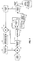
- a stored array of input image signals 8 which may be from any image, including scanned images or computer generated representations, directs input image I into the system on a signal by signal basis, where n,l represents the position of a single signal I n,l in a stream of image signals.
- I n,l refers in this description to both the signal that is positioned at n,l in the image signal stream, and the optical intensity or density of the image signal at position n,l.
- Each input signal has a corresponding error correction signal ⁇ added to the image signal I n,l at adder 10, where ⁇ n,l is a sum of weighted error term signals of previous pixels to be added to I n,l, resulting in a modified image signal, temporarily stored at block 12.
- the modified image signal is passed to threshold comparator 14.
- the modified image signal is compared to threshold T n,l to determine an appropriate output signal B n,l for pixel I n,l , such as, for example, in a binary output image, a spot or no spot.
- T n,l may vary in accordance with a dither pattern, or an edge enhancement scheme, or other threshold varying scheme.
- the value of signal B n,l is subtracted from the modified image signal (I n,l + ⁇ n,l ) to generate an error term signal ⁇ m from signal I n,l .
- the subtraction operation is represented by the change sign block 20 and subsequent adder 22, with error term signal ⁇ m representing the difference between the modified image signal (I n,l + ⁇ n,l ) and the output signal B n,l stored to error fraction determination block 24, where weighted portions of error term ⁇ m are calculated, and will be used for updating the error delay buffer 28.
- preliminary output signals B' n,l are directed to counter 40, which, when enabled, counts from 1 to a selected number N. Upon reaching N, counter 40 generates an enable signal TRAN EN for the output determinator 42. When enabled, output determinator 42 relays the preliminary output signal B' n,l to output image storage 16. In doing so, output determinator 42 compares each pixel with its predecessor to determine whether a transition from one level to another has occurred. In a binary system, a transition occurs when image signal B' n,l changes from a first state, represented by 1 or ON, to a second state, represented by 0 or OFF, and vice versa.
- output determinator 42 Upon detecting transition from first to second state in its enabled state, output determinator 42 generates a counter start signal C START to start counter 40 counting from 1-N, thereby disabling the output determinator input TRAN EN .
- the output of output determinator 42 is now maintained at a second state until the counter 40 enables the input TRAN EN and a transition is detected in B' n,l , whereupon, the output is changed and a start signal is sent to the counter.
- the output of output determinator 42 is connected to output image storage 16 for eventual transfer to a print buffer along line 18. It will be appreciated that, conveniently, at the beginning of an image, the state may be set to 0 or OFF at the output determinator, and the counter may start counting from an enabled condition.
- Value N is selected based on minimum desired spot size, and may reflect the printing process used. Thus, for example, if a minimum spot size of 2 pixels is required in a K x K standard process, N in a similar high addressability operating at K X 4K system will reflect that size, N will be 8. In general, however, the number N will not correspond to an integer number of pixels in the standard resolution. In one possible embodiment, the value of N may be different for white pixels and black pixels. Thus, in the given example, N may be 8 for black pixels, and 6 for white pixels.
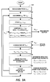
- steps 110, 120, 130, 140, 150, 160, 170 and 180 are a standard error diffusion method to obtain a binary image output from gray image input of: 110) receiving an image signal having a gray value I n,l ; 120) adding an error term ⁇ n,l from the error delay buffer to the image signal I n,l ; 130) storing the image signal I n,l + ⁇ n,l as a modified image signal; 140) thresholding the modified image signal against with signal T n,l to obtain a preliminary output signal B' n,l and directing B n,l to the output, where the threshold T n,l
- the unprocessed pixel set ⁇ I n+1,l , I n-1,l+1 , I nl+1 , I n+1,l+1 ⁇ shown associated with steps 170 and 180 is a common set for error diffusion, but other sets are also possible and are intended to be included in this description.
- step 140 and step 150 of Figure 3A are separated and the output of step 140 is relayed as preliminary output signal B' n,l to output determination step 200 shown in Figure 3B, at step 202.
- the signal B' n,l is either 1 or 0, the two members of the binary set of output values.
- the current state counter is incremented at step 250 and the actual output is relayed to step 270 to be incorporated in the computation of step 150 in Figure 3A.
- step 230 determines whether transition is enabled from counter step 300 shown in Figure 3C. On finding that a transition is disabled, the actual output is set to the previous output at step 241. The current state counter is again incremented at step 250 and the actual output is relayed to step 270 for subsequent use by step 150. If a transition was enabled by counter step 300 at step 230, the actual output is set to the preliminary output at step 242, the counter for the state after the transition is started at step 260 and the actual output is again relayed to step 270.
- Figure 3C shows an embodiment of the counter step 300 with inputs "increment current counter" from 250 and "counter reset" from step 260.
- the current counter is determined at step 310 through current counter memory 320.
- Step 330 increments the current counter LV1 or LV2 counters 335.
- Step 340 compares the current counter value with the minimum number NLVi of contiguous high addressability pixels required for same state and step 350 sets the transition enable flag to "YES” if the minimum number stored in NLVi storage 345 is reached. Otherwise step 360 sets the transition enable flag to "NO”.
- the change current counter step 370 changes the state of the current counter memory 320. Additionally the counter LVi is set to its start condition by reset counter block 380 and the transition enable flag is set to "NO" at step 360.
- the transition enable flag serves as input to transition enabled step 230 of Figure 3B.
Applications Claiming Priority (2)
| Application Number | Priority Date | Filing Date | Title |
|---|---|---|---|
| US922421 | 1986-10-23 | ||
| US07/922,421 US5374997A (en) | 1992-07-31 | 1992-07-31 | High addressability error diffusion with minimum mark size |
Publications (3)
| Publication Number | Publication Date |
|---|---|
| EP0581561A2 true EP0581561A2 (fr) | 1994-02-02 |
| EP0581561A3 EP0581561A3 (fr) | 1994-02-23 |
| EP0581561B1 EP0581561B1 (fr) | 1997-04-09 |
Family
ID=25447015
Family Applications (1)
| Application Number | Title | Priority Date | Filing Date |
|---|---|---|---|
| EP93305894A Expired - Lifetime EP0581561B1 (fr) | 1992-07-31 | 1993-07-26 | Diffusion d'erreurs à haute adressabilité et à taille de marque minimum |
Country Status (4)
| Country | Link |
|---|---|
| US (1) | US5374997A (fr) |
| EP (1) | EP0581561B1 (fr) |
| JP (1) | JPH06113124A (fr) |
| DE (1) | DE69309571T2 (fr) |
Cited By (3)
| Publication number | Priority date | Publication date | Assignee | Title |
|---|---|---|---|---|
| US5818971A (en) * | 1995-11-30 | 1998-10-06 | Oce-Nederland B.V. | Method and image reproduction device for reproducing grey values using a combination of error diffusion and cluster dithering for enhanced resolution and tone |
| US6353687B1 (en) * | 1998-12-18 | 2002-03-05 | Xerox Corporation | System and apparatus for single subpixel elimination with local error compensation in an high addressable error diffusion process |
| US6608700B1 (en) | 1999-11-24 | 2003-08-19 | Xerox Corporation | Removal of error diffusion artifacts with alternating distribution weights |
Families Citing this family (17)
| Publication number | Priority date | Publication date | Assignee | Title |
|---|---|---|---|---|
| US5611022A (en) * | 1993-07-07 | 1997-03-11 | Dataproducts Corporation | Color imaging |
| US5732162A (en) * | 1993-10-28 | 1998-03-24 | Xerox Corporation | Two dimensional linearity and registration error correction in a hyperacuity printer |
| KR0150150B1 (ko) * | 1994-07-14 | 1998-10-15 | 김광호 | 에지 강조를 이루는 오차확산 방식 이치화 방법 및 장치 |
| US5809177A (en) * | 1996-06-06 | 1998-09-15 | Xerox Corporation | Hybrid error diffusion pattern shifting reduction using programmable threshold perturbation |
| US5835687A (en) * | 1996-10-21 | 1998-11-10 | Vidar Systems Corporation | Methods and apparatus for providing digital halftone images with random error diffusion dithering |
| US6068361A (en) * | 1997-10-30 | 2000-05-30 | Mantell; David A. | Method and apparatus for multiple drop error diffusion in a liquid ink printer |
| US6856702B2 (en) * | 2001-06-28 | 2005-02-15 | Andrew C. Gallagher | System and method for selecting an image processing path using estimated appearance of noise |
| EP1331804A3 (fr) * | 2002-01-24 | 2003-11-19 | Ricoh Company, Ltd. | Dispositif et procédé de formation d'images, programme d'ordinateur et support d'enregistrement |
| US20040090654A1 (en) * | 2002-09-17 | 2004-05-13 | Luc Minnebo | FM screening with sub-dot phase modulation |
| EP1401189A1 (fr) * | 2002-09-17 | 2004-03-24 | Agfa-Gevaert | Tramage à modulation de fréquence et à modulation de phase des sous-points |
| KR100462633B1 (ko) * | 2003-02-17 | 2004-12-23 | 삼성전자주식회사 | 소수화소의 위치 정보를 이용한 이진영상 생성방법 |
| US7152964B2 (en) * | 2003-05-21 | 2006-12-26 | Eastman Kodak Company | Very high speed printing using selective deflection droplet separation |
| US8208175B2 (en) * | 2005-04-13 | 2012-06-26 | Xerox Corporation | Blended error diffusion and adaptive quantization |
| US7480078B2 (en) * | 2005-04-28 | 2009-01-20 | Xerox Corporation | Method and system for performing multi-pixel parallel error diffusion enabling high-speed diffusion processing without increasing the system clock rate |
| US7460727B2 (en) * | 2005-06-30 | 2008-12-02 | Xerox Corporation | Error diffusion method and hardware architecture |
| US7565027B2 (en) * | 2005-10-07 | 2009-07-21 | Xerox Corporation | Countdown stamp error diffusion |
| US8482801B2 (en) * | 2008-04-10 | 2013-07-09 | Xerox Corporation | Storage of stamp information for error diffusion |
Citations (2)
| Publication number | Priority date | Publication date | Assignee | Title |
|---|---|---|---|---|
| EP0333520A2 (fr) * | 1988-03-18 | 1989-09-20 | Matsushita Electric Industrial Co., Ltd. | Appareil de traitement des signaux à deux niveaux pour l'affichage d'images |
| WO1990009075A2 (fr) * | 1989-01-30 | 1990-08-09 | Eastman Kodak Company | Formation de demi-teintes numeriques par diffusion d'erreur |
Family Cites Families (7)
| Publication number | Priority date | Publication date | Assignee | Title |
|---|---|---|---|---|
| EP0031247B1 (fr) * | 1979-12-20 | 1984-03-14 | Cambridge Consultants Limited | Dispositif et procédé pour la fabrication d'une image demi-ton se composant de points dispersés à partir d'une image sans graduation |
| US4654721A (en) * | 1985-04-12 | 1987-03-31 | International Business Machines Corporation | System for reproducing multi-level digital images on a bi-level printer of fixed dot size |
| US4955065A (en) * | 1987-03-17 | 1990-09-04 | Digital Equipment Corporation | System for producing dithered images from continuous-tone image data |
| US5045952A (en) * | 1989-08-21 | 1991-09-03 | Xerox Corporation | Method for edge enhanced error diffusion |
| US5025322A (en) * | 1989-12-18 | 1991-06-18 | Eastman Kodak Company | Method and apparatus for grey level recording using multiple addressability |
| US5221971A (en) * | 1990-11-21 | 1993-06-22 | Polaroid Corporation | Area modulation printing apparatus |
| US5274472A (en) * | 1992-05-21 | 1993-12-28 | Xerox Corporation | High addressability image generator using pseudo interpolation of video and screen data |
-
1992
- 1992-07-31 US US07/922,421 patent/US5374997A/en not_active Expired - Fee Related
-
1993
- 1993-06-14 JP JP5167503A patent/JPH06113124A/ja not_active Withdrawn
- 1993-07-26 DE DE69309571T patent/DE69309571T2/de not_active Expired - Fee Related
- 1993-07-26 EP EP93305894A patent/EP0581561B1/fr not_active Expired - Lifetime
Patent Citations (2)
| Publication number | Priority date | Publication date | Assignee | Title |
|---|---|---|---|---|
| EP0333520A2 (fr) * | 1988-03-18 | 1989-09-20 | Matsushita Electric Industrial Co., Ltd. | Appareil de traitement des signaux à deux niveaux pour l'affichage d'images |
| WO1990009075A2 (fr) * | 1989-01-30 | 1990-08-09 | Eastman Kodak Company | Formation de demi-teintes numeriques par diffusion d'erreur |
Cited By (3)
| Publication number | Priority date | Publication date | Assignee | Title |
|---|---|---|---|---|
| US5818971A (en) * | 1995-11-30 | 1998-10-06 | Oce-Nederland B.V. | Method and image reproduction device for reproducing grey values using a combination of error diffusion and cluster dithering for enhanced resolution and tone |
| US6353687B1 (en) * | 1998-12-18 | 2002-03-05 | Xerox Corporation | System and apparatus for single subpixel elimination with local error compensation in an high addressable error diffusion process |
| US6608700B1 (en) | 1999-11-24 | 2003-08-19 | Xerox Corporation | Removal of error diffusion artifacts with alternating distribution weights |
Also Published As
| Publication number | Publication date |
|---|---|
| JPH06113124A (ja) | 1994-04-22 |
| EP0581561B1 (fr) | 1997-04-09 |
| DE69309571D1 (de) | 1997-05-15 |
| EP0581561A3 (fr) | 1994-02-23 |
| US5374997A (en) | 1994-12-20 |
| DE69309571T2 (de) | 1997-11-27 |
Similar Documents
| Publication | Publication Date | Title |
|---|---|---|
| EP0581561B1 (fr) | Diffusion d'erreurs à haute adressabilité et à taille de marque minimum | |
| EP0602854B1 (fr) | Demi-teinte en groupes avec diffusion des erreurs de point à point | |
| US5325211A (en) | Error diffusion with output and input based feedback | |
| US5535019A (en) | Error diffusion halftoning with homogeneous response in high/low intensity image regions | |
| EP0544511B1 (fr) | Obtention de demi-teintes à plage dynamique améliorée et à diffusion d'erreurs améliorant les contours | |
| EP0531170B1 (fr) | Méthode de quantification de données de pixel à tonalité de gris avec mise en oeuvre de diffusion d'erreur sous compensée | |
| US5243443A (en) | Halftoning with error feedback and image dependent enhancement | |
| US5565994A (en) | Multiple separation error diffusion, with cross separation correlation control for color images | |
| EP0833499B1 (fr) | Traitement d'images en couleurs séparation à séparation utilisant la diffusion d'erreurs | |
| US5226096A (en) | Digital halftoning with selectively applied dot-to-dot error diffusion | |
| EP1505821B1 (fr) | Appareil et procédé de traitement d'images et appareil de formation d'images | |
| US5353127A (en) | Method for quantization gray level pixel data with extended distribution set | |
| US5604605A (en) | Method and device for intralinearly halftoning digitized grey value images | |
| US6068361A (en) | Method and apparatus for multiple drop error diffusion in a liquid ink printer | |
| EP0774856B1 (fr) | Système et procédé pour obtenir un système d'impression avec haute adressabilité | |
| EP0817466B1 (fr) | Diffusion des erreurs avec amélioration des bords | |
| US5784496A (en) | Error sum method and apparatus for intercolor separation control in a printing system | |
| US5598204A (en) | Image halftoning system capable of producing additional gradations | |
| EP0774855B1 (fr) | Procédé de conversion de projection en perspective | |
| US6873440B2 (en) | Multibit screening of print documents in a PDL environment | |
| US6141114A (en) | Edge enhanced error diffusion with artifact correction in areas of highlights and shadows | |
| EP1077572B1 (fr) | Appareil de formation d'images avec lissage des données d'image sélective | |
| JP3501533B2 (ja) | カラー画像形成装置 |
Legal Events
| Date | Code | Title | Description |
|---|---|---|---|
| PUAI | Public reference made under article 153(3) epc to a published international application that has entered the european phase |
Free format text: ORIGINAL CODE: 0009012 |
|
| PUAL | Search report despatched |
Free format text: ORIGINAL CODE: 0009013 |
|
| AK | Designated contracting states |
Kind code of ref document: A2 Designated state(s): DE FR GB |
|
| AK | Designated contracting states |
Kind code of ref document: A3 Designated state(s): DE FR GB |
|
| 17P | Request for examination filed |
Effective date: 19940802 |
|
| GRAG | Despatch of communication of intention to grant |
Free format text: ORIGINAL CODE: EPIDOS AGRA |
|
| 17Q | First examination report despatched |
Effective date: 19960902 |
|
| GRAH | Despatch of communication of intention to grant a patent |
Free format text: ORIGINAL CODE: EPIDOS IGRA |
|
| GRAH | Despatch of communication of intention to grant a patent |
Free format text: ORIGINAL CODE: EPIDOS IGRA |
|
| GRAA | (expected) grant |
Free format text: ORIGINAL CODE: 0009210 |
|
| AK | Designated contracting states |
Kind code of ref document: B1 Designated state(s): DE FR GB |
|
| REF | Corresponds to: |
Ref document number: 69309571 Country of ref document: DE Date of ref document: 19970515 |
|
| ET | Fr: translation filed | ||
| PLBE | No opposition filed within time limit |
Free format text: ORIGINAL CODE: 0009261 |
|
| STAA | Information on the status of an ep patent application or granted ep patent |
Free format text: STATUS: NO OPPOSITION FILED WITHIN TIME LIMIT |
|
| 26N | No opposition filed | ||
| PGFP | Annual fee paid to national office [announced via postgrant information from national office to epo] |
Ref country code: FR Payment date: 20010712 Year of fee payment: 9 |
|
| PGFP | Annual fee paid to national office [announced via postgrant information from national office to epo] |
Ref country code: DE Payment date: 20010716 Year of fee payment: 9 |
|
| PGFP | Annual fee paid to national office [announced via postgrant information from national office to epo] |
Ref country code: GB Payment date: 20010725 Year of fee payment: 9 |
|
| REG | Reference to a national code |
Ref country code: GB Ref legal event code: IF02 |
|
| PG25 | Lapsed in a contracting state [announced via postgrant information from national office to epo] |
Ref country code: GB Free format text: LAPSE BECAUSE OF NON-PAYMENT OF DUE FEES Effective date: 20020726 |
|
| PG25 | Lapsed in a contracting state [announced via postgrant information from national office to epo] |
Ref country code: DE Free format text: LAPSE BECAUSE OF NON-PAYMENT OF DUE FEES Effective date: 20030201 |
|
| GBPC | Gb: european patent ceased through non-payment of renewal fee |
Effective date: 20020726 |
|
| PG25 | Lapsed in a contracting state [announced via postgrant information from national office to epo] |
Ref country code: FR Free format text: LAPSE BECAUSE OF NON-PAYMENT OF DUE FEES Effective date: 20030331 |
|
| REG | Reference to a national code |
Ref country code: FR Ref legal event code: ST |