EP0579340A1 - Distanzschuts- und Fernmessungsvorrichtung für eine Hochspannungsübertragungsleitung - Google Patents
Distanzschuts- und Fernmessungsvorrichtung für eine Hochspannungsübertragungsleitung Download PDFInfo
- Publication number
- EP0579340A1 EP0579340A1 EP93202763A EP93202763A EP0579340A1 EP 0579340 A1 EP0579340 A1 EP 0579340A1 EP 93202763 A EP93202763 A EP 93202763A EP 93202763 A EP93202763 A EP 93202763A EP 0579340 A1 EP0579340 A1 EP 0579340A1
- Authority
- EP
- European Patent Office
- Prior art keywords
- signal
- input
- output
- circuit
- coupled
- Prior art date
- Legal status (The legal status is an assumption and is not a legal conclusion. Google has not performed a legal analysis and makes no representation as to the accuracy of the status listed.)
- Withdrawn
Links
Images


Classifications
-
- H—ELECTRICITY
- H02—GENERATION; CONVERSION OR DISTRIBUTION OF ELECTRIC POWER
- H02H—EMERGENCY PROTECTIVE CIRCUIT ARRANGEMENTS
- H02H3/00—Emergency protective circuit arrangements for automatic disconnection directly responsive to an undesired change from normal electric working condition with or without subsequent reconnection ; integrated protection
- H02H3/40—Emergency protective circuit arrangements for automatic disconnection directly responsive to an undesired change from normal electric working condition with or without subsequent reconnection ; integrated protection responsive to ratio of voltage and current
Definitions
- the present invention relates to protective systems for use in AC electrical power distribution systems and more particularly to distance relays for AC electrical power transmission line protection.
- Distance relays are well known in the art of protective relaying. For example, reference may be had to "The Art and Science of Protective Relaying", Mason, published by John Wiley and Son, Inc. (1956), particularly to Chapter 14. Exemplary types of distance relays are disclosed in U.S. Patent No. 4,034,269, issued to S. B. Wilkinson, on July 5, 1977; U.S. Patent No. 4,420,788, issued to S. B. Wilkinson and G. E. Alexander on December 13, 1983; and U.S. Patent No. 4,405,966, issued to Leonardo Cavero, the inventor of the present invention, on September 20, 1983. All these patents are assigned to the assignee of the present invention and are incorporated by reference in the present application as if fully set forth herein.
- Distance relays are utilized in protective systems for AC power transmission lines to detect faults within protected zones or portions of the transmission lines. If such a fault is detected within the relay's zone or reach, the distance relay will enable operation of a circuit breaker in order to trip the faulted phase or phases.
- Phase distance relays are utilized to detect phase to phase faults within a protected zone or portion of a transmission line. If such a fault is detected within the zone or reach of this type of distance relay, the phase distance relay will initiate a signal which will be used to cause the operation of a three pole circuit breaker to trip all three phases of the transmission line. This is to be contrasted with a ground distance relay which detects faults between a phase and ground, again within a designated zone or reach; and, upon detection of such a fault, generates a signal which enables the operation of a circuit breaker to trip the faulted phase only.
- each particular distance relay should only detect faults within its protected zone or reach.
- the parameters of a distance relay are commonly selected to correspond to the parameters of the transmission line. For example, the parameters are selected to provide a forward reach that may correspond to the forward distance of the protected zone of a transmission line under protection of the particular relay. It is desired that the distance relay operate within its selected forward reach thereby confining the protection of a particular distance relay to the selected zone within a protected system.
- the desired operation of the distance relay may be hindered by the inability to distinguish between internal and external faults.
- Internal faults are those which occur within the protected zone or reach of the relay, whereas external faults are those which occur outside the zone or relay reach.
- errors in measuring fault resistance can cause the fault to appear further away from or closer to the distance relay location than it actually is; situations which, in the worse case, could prevent the operation of the distance relay on a fault occurring within its zone or reach, or could cause the relay to misoperate for a fault external to the protected zone or reach.
- distance relays have, in the past, been used to detect faults within a predetermined protected zone or reach of the relay, such relays have not been able to provide a determination of the actual location of the fault; that is, the distance from the relay at which the fault occurred.
- the ability to determine the location of the fault in terms of distance from the relay enhances the utility of a distance relay.
- Embodiments of the invention seek to provide one or more of the following features: a distance relay with improved discrimination between internal and external faults thereby increasing the reliability of the relay operation and the security of the protection system; a distance relay for detecting faults in a protected zone of an AC electrical power transmission line, which relay determines the distance to the fault; a distance relay with a capability for improved fault resistance determination; a distance relay which substantially eliminates the adverse effects on fault distance determination due to fault current components from multiple sources connected to the AC power transmission line; a distance relay which eliminates adverse effects of prefault load current on fault distance determination.
- the present invention comprises a distance relay for detecting faults within a predetermined protected zone of an AC electrical power transmission line and for measuring the distance to detected faults.
- the distance relay includes means for detecting a fault current and subtracting prefault current therefrom.
- Figure 1 is a one line, block diagram of a current and voltage processing portion of a preferred embodiment of the present invention.
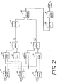
- Figure 2 is a block diagram of a first operate signal generation portion of the preferred embodiment of the present invention, utilizing voltage and current signals generated by that portion depicted in Figure 1.
- Figure 3 is a block diagram of a distance measurement portion of the preferred embodiment of the present invention, utilizing voltage and current signals generated by the portion depicted in Figure 1.
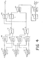
- Figure 4 is a block diagram of a second operate signal generation portion of the preferred embodiment of the present invention, utilizing voltage and current signals generated by that portion depicted in Figure 1.
- Figure 5 is a block diagram of a trip signal generation portion of the preferred embodiment of the present invention, utilizing the first and second operate signals generated by that portion depicted in Figures 2 and 4 respectively.
- Figure 6 depicts the characteristic of the preferred embodiment of the relay of the present invention plotted on an L-R diagram.
- Figure 7 is a block diagram of a third operate signal generation portion of the preferred embodiment of the present invention, utilizing a delta current signal generated by that portion depicted in Figure 1 and signals generated by the second operate signal generation portion depicted in Figure 4.
- Figure 8 is a one line, block diagram of an current and voltage processing portion of an alternate preferred embodiment of the present invention.
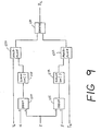
- Figure 9 is a block diagram of a distance impedance measurement portion of the alternate preferred embodiment of the present invention, utilizing voltage and current signals generated by that portion depicted in Figure 8.
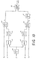
- Figure 10 is a block diagram of a distance protection portion of the alternate preferred embodiment of the present invention, utilizing voltage and current signals generated by that portion depicted in Figure 8.
- Figure 11 is a block diagram of a distance protection, resistance reach and measurement portion of the alternate preferred embodiment of the present invention, utilizing voltage and current signals generated by that portion depicted in Figure 8.
- Figure 12 is a block diagram of a trip signal generation portion of the alternate preferred embodiment of the present invention, utilizing the operate signals generated by that portion depicted in Figures 10 and 11.
- Figure 13 depicts the characteristic of the alternate preferred embodiment of the relay of the present invention plotted on an L-R diagram.
- Figure 14 is a block diagram of a preferred embodiment of a fault resistance measurement portion of the present invention.
- Figure 15 is a block diagram of an alternate preferred embodiment of a resistance measurement portion of the present invention.
- an alternating current electric power transmission line generally designated 10.
- alternating current electrical power transmission lines normally comprise three phases and ground, for purposes of simplicity and clarity, the following detailed description will be described with respect to the A phase (A) and ground (G). It should be understood that the following description also applies with respect to the B and the C phase, as well as relays connected between phases.
- phase Associated with A phase is means 12 for sensing current in that phase as well as means 14 for sensing voltage on that phase.
- current sensing means 12 may be a current transformer and voltage sensing means 14 may be a step down potential transformer.
- a current sensing means may be associated with each phase as well as a separate voltage sensing means associated with each phase.
- FIG. 1 it is to be understood that although a specific type of current and voltage sensing scheme is depicted in Figure 1, other schemes known in the art may be substituted for that depicted; the purpose being to obtain signals which are related to each phase voltage and each phase current.
- the first 16 and second 18 low pass filters each preferably have a frequency cut off of approximately 500Hz in order to filter out transients and other spurious signals having frequencies which exceed 1KHz, while passing, substantially unchanged, signals at the system frequency which is typically 50Hz or 60Hz. Consequently, the output signal i A (t) from the first filter 16 is the filtered input signal i A (t), and the output signal v A (t) from the second filter 18 is the filtered input signal v A (t).
- the output v A (t) of the second low pass filter 18 is coupled to the input of a first analog to digital (A/D) converter 20.
- the first A/D converter 20 samples the magnitude of the input signal at a predetermined rate which in the preferred embodiment, is twenty samples per cycle in 50Hz systems and sixteen samples per cycle in 60 Hz systems. The magnitude of each sample is converted into a digital signal having a value corresponding to such magnitude. Consequently, the output v A (t) of the first A/D converter 20 is a digitized version of the analog input signal.
- the output of the first low pass filter 16 is coupembodiment, the second A/D converter 22 is of the same type and performs the same function as that previously described with respect to the first A/D converter 20.
- the output i A (t) of the second A/D converter 22, which is a digitized version of the input signal, is coupled to the input of a buffer 24, a positive input of a first digital subtraction circuit 26, the input of a first differentiator 28, and the input of a first scaler 30.
- the buffer 24 comprises a memory for storing the digitized input signal i A (t) for a time k/f where k is a predetermined constant and f is the system frequency, typically 50 Hz or 60 Hz.
- the output of the buffer 24 is the signal i A (t-k/f) .
- the output of the buffer 24 is equal to the magnitude of i A at a point one cycle prior to the input i A (t).
- the output i A (t-k/f) of buffer 24 is the input signal i A (t) which has been delayed five cycles at the fundamental system frequency; that is, 100 milliseconds in a 50Hz system and 83.333 milliseconds in a 60Hz system.
- the output i A (t-k/f) of the buffer 24 is coupled to a negative input of the first digital subtraction circuit 26.
- the first digital subtraction circuit 26 is a circuit whose output is a digital signal ⁇ i A (t) having a digital value equal to the magnitude of the digital value of the input signal applied to the positive input minus the value of the signal applied to the negative input. Since the signal i A (t) is applied to the positive input and the signal i A (t-k/f) is applied to the negative input, the output signal, ⁇ i A (t) is equal to i A (t)-i A (t-k/f) .
- the output ⁇ i A (t) of the digital subtraction circuit 26 is coupled to the input of a second differentiator 32 and one input of a first two-input adder 34.
- the first 28 and second 32 differentiators each measures and stores the magnitude of the input signal at a first time t1 and again at a second time t3, then subtracts the magnitude measured at t1 from the magnitude measured at t3 and divides the result by the magnitude of time t3 minus time t1. Consequently, the output of the second digital differentiator 32 is a signal at a time t2, having a value substantially equal to the differential, with respect to time, of the input signal ⁇ i A (t).
- the output of the second digital differentiator 32 is coupled to the input of a second scaler 36.
- the second scaler 36 is a circuit whose output is a digital signal having a magnitude equal to the input signal multiplied by a predetermined scaler function which, in the preferred embodiment is where f is the fundamental system frequency, typically 50Hz or 60Hz, and tan ⁇ is a quantity which is a function of the particular power system in which the distance relay of the present invention is used. Consequently the output of the second scaler 36 is
- the output of the second scaler 36 is coupled to the second input of the first two-input adder 34.
- the first two-input adder 34 is a circuit whose output is a digital signal i f (t) having a magnitude which is equal to the digital sum of the input signals which are ⁇ i A (t) and Consequently, the output i f (f) of the first two-input adder 34 is equal to
- the output of the first differentiator 28 is a digital signal whose magnitude is the differential respect to time of the input signal i A (t).
- the output of the first differentiator 28 is coupled to the input of a third scaler 38.
- the third scaler 38 is of the same type as that previously described with respect to the first 30 and second 36 scalers, having a digital output signal whose magnitude is equal to the input multiplied by a predetermined scaling function which, in the preferred embodiment, is L. Consequently, the output of the third scaler 38 is The magnitude of L is selected to be substantially equal to the line inductance per mile of the particular power system in which the relay of the present invention is used.
- the output of the third scaler 38 is coupled to one input of a second two input adder 40.
- the output of the first scaler 30 is a digital signal whose magnitude is equal to the input signal i A (t) multiplied by a predetermined scaling function which, in the preferred embodiment, is R. Consequently, the output of the first scaler 30 is Ri A (t).
- the magnitude of R is selected to be substantially equal to the line resistance per mile of the particular power system in which the relay of the present invention is used.
- the output Ri A (t) of the first scaler 30 is coupled to the second input of the second two input adder 40.
- the second two input adder 40 is the same type as that previously described with respect to the first two input adder 34, having an output signal whose magnitude is equal to the sum of the inputs Ri A (t) and Accordingly, v r (t) is equal to
- the output signal i f (t) from the first two-input adder 34 is coupled to the input of the first sampler/buffer circuit 42.
- the output v r (t) from the second two-input adder 40 is coupled to the input of a second sampler/buffer circuit 44.
- the output v A (t) of the first A/D converter 20 is coupled to the input of a third sampler/buffer circuit 46.
- the first 42, second 44 and third 46 sampler/buffer circuits each have two outputs, the first of which is equal to the magnitude of the input signal sampled at a first time t1, and the second of which is equal to the magnitude of the input signal sampled at a second time t2. Consequently, the outputs of the first sampler/buffer circuit 42 is a first signal i f (t1) which is the input signal i f (t) sampled at time t1; and the second output is a signal i f (t2) which is equal to the input signal i f (t) sampled at time t2.
- the outputs of the second sampler/buffer circuit 44 comprise a first signal v r (t1) which is equal to the input signal v r (t) sampled at the first time t1; and a second signal v r (t2) which is equal to the input signal v r (t) sampled at the second time t2.
- the outputs of the third sampler/buffer circuit 46 comprise a first signal v A (t1) which is equal to the input signal v A (t) sampled at the first time t1; and a second signal v A (t2) which is equal to the input signal v A (t) sampled at the second time t2.
- the output signal i f (t1) from the first sampler/buffer circuit 42 is coupled to one input of a first two-input multiplier 48 and one input of a second two-input multiplier 50.
- the output signal i f (t2) from the first sampler/buffer circuit 42 is coupled to one input of a third two-input multiplier 52 and one input of a fourth two-input multiplier 54.
- the output signal v r (t1) from the second sampler/buffer circuit 44 is coupled to the second input of the third two-input multiplier 52.
- the output signal v r (t2) from the second sampler/buffer circuit 44 is coupled to the second input of the first two-input multiplier 48.
- the output signal v A (t1) from the third sampler/buffer circuit 46 is coupled to the second input of the fourth two-input multiplier 54.
- the output signal v A (t2) from the third sampler/buffer circuit 46 is coupled to the second input of the second two-input multiplier 50.
- the first 48, second 50, third 52 and fourth 54 two-input multipliers are each digital multipliers producing a digital output signal having a magnitude which is equal to the magnitude of the first input signal multiplied by the magnitude of the second input signal. Consequently, the output of the first multiplier 48 is the signal v r (t2)i f (t1); the output of the second multiplier circuit 50 is the signal v A (t2)i f (t1); the output of the third multiplier 52 is the signal v r (t1)i f (t2); and the output of the fourth multiplier 54 is the signal v A (t1)i f (t2).
- the output of the first multiplier circuit 48 is coupled to a negative input of a second digital subtraction circuit 60.
- the output of the second multiplier circuit 50 is coupled to a negative input of a third digital subtraction circuit 62.
- the output of the third multiplier circuit 52 is coupled to a positive input of the second digital subtraction circuit 60.
- the output of the fourth multiplier circuit 54 is coupled to a positive input of the third digital subtraction circuit 62.
- the second 60 and third 62 digital subtraction circuits are of the same type as the previously described first digital subtraction circuit 26, each producing a digital output signal whose magnitude is equal to the magnitude of the signal applied to the positive input minus the magnitude of the signal applied to the negative input.
- the output of the second digital subtraction circuit 60 is the signal S1 which is is equal to v r (t1)i f (t2)-v r (t2)i f (t1); and the output of the third digital subtraction circuit 62 is the signal S2 which is equal to v A (t1)i f (t2)-v A (t2)i f (t1).
- the output signal S1 from the second digital subtraction circuit 60 is coupled to the input of a fourth scaler circuit 64.
- the fourth scaler circuit 64 is preferably of the same type as that previously described with respect to the first 30, second 36 and third 38 scaler circuits, having an output which is equal to the input multiplied by a predetermined scaling function.
- the scaling function of the fourth scaler circuit 64 is the quantity n set which is a constant determined by the desired relay reach. Consequently, the output of the fourth scaler circuit 64 is the signal n set ⁇ v r (t1)i f (t2)-v r (t2)i f (t1) ⁇ or n set S1.
- the output of the fourth scaler circuit 64 is coupled to a first input of a first two-input comparator circuit 66.
- the output of the third digital subtraction circuit 62 is coupled to a second input of the first two-input comparator circuit 66.
- the first two-input comparator circuit 66 is a digital comparator which generates an output signal when the magnitude of the signal applied to the first input exceeds the magnitude of the signal applied to the second input.
- the first two-input comparator circuit 66 generates an output signal when the magnitude of the signal n set ⁇ v r (t1)i f (t2)-v r (t2)i f (t1) ⁇ exceeds the magnitude of the signal ⁇ v A (t1)i f (t2)-v A (t2)i f (t1) ⁇ or n set S1>S2.
- the output of the first two-input comparator circuit 66 is coupled to the input of a first counter 68.
- the first counter 68 provides a count signal upon receipt of a signal from the first two-input comparator circuit 66.
- the count signal is incremented by one count if the signal from the circuit 66 is present during the next succeeding sampling interval; otherwise, the count signal is reset to zero.
- the count signal is incremented by one count upon receipt of a signal from circuit 66 during each succeeding sampling interval.
- the count signal is reset to zero following any sampling interval during which a signal is not received from circuit 66.
- the count signal from the first counter 68 is coupled to the input of a first comparator circuit 70.
- the first comparator circuit 70 generates an output signal O1, which is a first operate signal in the preferred embodiment described herein, when the magnitude of the input signal exceeds a predetermined value. Consequently, the first comparator circuit 70 will generate the first operate signal O1 when the magnitude of the count signal from the counter 68 exceeds a predetermined value, for example three in the preferred embodiment. This means that in the preferred embodiment, the first operate signal O1 will be generated upon detection of a signal from the first two-input comparator circuit 66 during at least three consecutive sampling intervals.
- the output signal ⁇ i A (t) from the first digital subtraction circuit 26 is coupled to the input of a fourth sampler/buffer circuit 202.
- the output V r (t) from the second two input adder 40 is coupled to the input of a fifth sampler/buffer circuit 204.
- the output v A (t) of the first A/D converter 20 is coupled to the input of a sixth sampler/buffer circuit 206.
- the fourth 202, fifth 204 and sixth 206 sampler/buffer circuits are of the same type as the first 42, second 44 and third 46 sampler/buffer circuits previously described.
- the outputs of the fourth sampler/buffer circuit 202 is a first signal ⁇ i A (t1) which is the input signal ⁇ i A (t) sampled at the first time t1; and the second output is a signal ⁇ i A (t2) which is equal to the input signal ⁇ i A (t) sampled at the second time t2.
- the outputs of the fifth sampler/buffer circuit 204 comprise a first signal V r (t1) which is equal to the input signal V r (t) sampled at the first time t1; and a second signal V r (t2) which is equal to the input signal V r (t) sampled at the second time t2.
- the outputs of the sixth sampler/buffer circuit 206 comprise a first signal v A (t1) which is equal to the input signal v A (t) sampled at the first time t1; and a second signal v A (t2) which is equal to the input signal v A (t) sampled at the second time t2.
- the signal ⁇ i A (t1) output from the fourth sampler/buffer circuit 202 is coupled to one input of a fifth two-input multiplier 208 and one input of a sixth two-input multiplier 210.
- the signal ⁇ i A (t2) output from the fourth sampler/buffer circuit 202 is coupled to one input of a seventh two-input multiplier 212 and one input of an eighth two-input multiplier 214.
- the V r (t1) signal output from the fifth sampler/buffer circuit 204 is coupled to the second input of the seventh two-input multiplier 212.
- the signal V r (t2) output from the fifth sampler/buffer circuit 204 is coupled to the second input of the fifth two-input multiplier 208.
- the signal v A (t1) output from the sixth sampler/buffer circuit 206 is coupled to the second input of the eighth two-input multiplier 214.
- the signal v A (t2) output from the sixth sampler/buffer circuit 206 is coupled to the second input of the sixth two-input multiplier 210.
- the fifth 208, sixth 210, seventh 212 and eighth 214 two-input multipliers are the same type as the first 48, second 50, third 52 and fourth 54 two-input multipliers previously described.
- Each two-input multiplier produces a digital output signal having a magnitude which is equal to the magnitude of the first input signal multiplied by the magnitude of the second input signal.
- the output of the fifth multiplier 208 is the signal V r (t2) ⁇ i A (t1); the output of the sixth multiplier circuit 210 is the signal v A (t2) ⁇ i A (t1); the output of the seventh multiplier 212 is the signal V r (t1) ⁇ i A (t2); and the output of the eighth multiplier 214 is the signal v A (t1) ⁇ i A (t2).
- the output of the fifth multiplier circuit 208 is connected to a negative input of a fourth digital subtraction circuit 216.
- the output of the sixth multiplier circuit 210 is coupled to a negative input of a fifth digital subtraction circuit 218.
- the output of the seventh multiplier circuit 212 is coupled to a positive input of the fourth digital subtraction circuit 216.
- the output of the eighth multiplier circuit 214 is coupled to a positive input of the fifth digital subtraction circuit 218.
- the fourth 216 and fifth 218 digital subtraction circuits are of the same type as the previously described first 26, second 60 and third 62 digital subtraction circuits, with each producing a digital output signal whose magnitude is equal to the magnitude of the signal applied to the positive input minus the magnitude of the signal applied to the negative input.
- the output signal S3 of the fourth digital subtraction circuit 216 is equal to V r (t1) ⁇ i A (t2)-V r (t2) ⁇ i A (t1); and the output signal S4 of the fifth digital subtraction circuit 218 is equal to V A (t1) ⁇ i A (t2)-V A (t2) ⁇ i A (t1).
- the output signal S3 of the fourth digital subtraction circuit 216 is coupled to the divisor input of a digital divider circuit 220.
- the output signal S4 of the fifth digital subtraction circuit 218 is coupled to a dividend input of the digital divider 220.
- the output n from the divider circuit 220 is a digital signal whose magnitude is equal to the quotion of the digital signal S4 applied to the dividend input divided by the digital signal S3 applied to the divisor input.
- the magnitude of the signal n is a function of the distance from the relay to the fault and is equal to
- the output signal ⁇ i A (t) from the first digital subtraction circuit 26 is coupled to the input of a seventh sampler/buffer circuit 402.
- the output V r (t) from the second two-input adder 40 is coupled to the input of an eighth sampler/buffer circuit 404.
- the output v A (t) of the first A/D converter 20 is coupled to the input of a ninth sampler/buffer circuit 406.
- the seventh 402, eighth 404 and ninth 406 sampler/buffer circuits are of the same type as the first 42, second 44, third 46, fourth 202, fifth 204 and sixth 206 sampler/buffer circuits previously described.
- the outputs of the seventh sampler/buffer circuit 402 is a first signal ⁇ i A (t1) which is the input signal ⁇ i A (t) sampled at the first time t1; and the second output is a signal ⁇ i A (t2) which is equal to the input signal ⁇ i A (t) sampled at the second time t2.
- the outputs of the eighth sampler/buffer circuit 404 comprises a first signal V r (t1) which is equal to the input signal V r (t) sampled at the first time t1; and a second signal V r (t2) which is equal to the input signal V r (t) sampled at the second time t2.
- the outputs of the ninth sampler/buffer circuit 406 comprises a first signal v A (t1) which is equal to the input signal v A (t) sampled at the first time t1; and a second signal v A (t2) which is equal to the input signal v A (t) sampled at the second time t2.
- the signal ⁇ i A (t1) output from the seventh sampler/buffer circuit 402 is coupled to one input of a two-input multiplier 408.
- the signal ⁇ i A (t2) output from the seventh sampler/buffer circuit 402 is coupled to one input of a tenth two-input multiplier 410.
- the V r (t1) signal output from the eighth sampler/buffer circuit 404 is coupled to the second input of the tenth two-input multiplier 410 and to one input of an eleventh two-input multiplier 412.
- the V r (t2) signal output from the eighth sampler/buffer circuit 404 is coupled to a second input of the ninth two-input multiplier 408 and one input of a twelfth two-input multiplier 414.
- the v A (t1) signal output from the ninth sampler/buffer circuit 406 is coupled to a second input of the twelfth two-input multiplier 414.
- the v A (t2) signal output from the ninth sampler/buffer circuit 406 is coupled to a second input of the eleventh two-input multiplier 412.
- the ninth 408, tenth 410, eleventh 412 and twelfth 414 two-input multipliers are the same type as the first 48 through eighth 214 two-input multipliers previously described.
- Each two-input multiplier produces a digital output signal having a magnitude which is equal to the magnitude of the first input signal multiplied by the magnitude of the second input signal.
- the output of the ninth multiplier 408 is the signal v r (t2) ⁇ i A (t1); the output of the tenth multiplier 410 is the signal v r (t1) ⁇ i A (t2); the output of the eleventh multiplier 412 is the signal v A (t2)v r (t1); and the output of the twelfth multiplier 414 is the signal v A (t1)v r (t2).
- the output of the ninth multiplier circuit 408 is connected to a positive input of a sixth digital subtraction circuit 416.
- the output of the tenth multiplier circuit 410 is coupled to a negative input of the sixth digital subtraction circuit 416.
- the output of the eleventh multiplier circuit 412 is coupled to a negative input of a seventh digital subtraction circuit 418.
- the output of the twelfth multiplier circuit 414 is coupled to the positive input the seventh digital subtraction circuit 418.
- the sixth 416 and seventh 418 digital subtraction circuits are of the same type as the previously described first 26, second 60, third 62, fourth 216 and fifth 218 digital subtraction circuits, with each providing a digital output signal whose magnitude is equal to the magnitude of the signal applied to the positive input minus the magnitude of the signal applied to the negative input. Consequently, the output signal S5 of the sixth digital subtraction circuit 416 is equal to v r (t2) ⁇ i A (t1)-v r (t1) ⁇ i A (t2); and the output signal S6 of the seventh digital subtraction circuit 418 is equal to v A (t1)V r (t2)-v A (t2)V r (t1).
- the output signal S5 of the sixth digital subtraction circuit 416 is coupled to the divisor input of a second digital divider circuit 420.
- the output signal S6 of the seventh digital subtraction circuit 418 is coupled to a dividend input of the second digital divider 420.
- the second digital divider 420 is the same type as the previously described first digital divider circuit 220; having an output signal which is a digital signal whose magnitude is equal to the quotion of the digital signal S6 applied to the dividend input divided by the digital signal S5 applied to the divisor input.
- the output R fA from the second divider circuit 420 is equal to
- the signal R fA is a function of the fault resistance; that is, the magnitude of R fA is proportional to the magnitude of the fault resistance measured at the relay location and the angle of the signal R fA is substantially equal to the fault resistance angle.
- the output signal S5 of the sixth digital subtraction circuit 416 is also coupled to the input of a fifth scaler circuit 422.
- the fifth scaler circuit 422 is preferably of the same type as that previously described with respect to the first 30, second 36, third 38 and fourth 64 scaler circuits, having an output which is equal to the input multiplied by a predetermined scaling function.
- the scaling function of the fifth scaler circuit 422 is the quantity R SET which is a constant determined by the desired relay reach. Consequently, the output of the fifth scaler circuit 222 is the signal R SET [ ⁇ i A (t1)V r (t2)- ⁇ i A (t2)V r (t1)] or R SET S5.
- the output of the fifth scaler circuit 422 is coupled to a first input of a second two-input comparator circuit 424.
- the output signal S4 of the seventh digital subtraction circuit 418 is coupled to a second input of the second two-input comparator circuit 424.
- the second two-input comparator circuit 424 is preferably of the same type as that previously described with respect to the first two-input comparator circuit 66 which generates an output signal when the magnitude of the signal applied to the first input exceeds the magnitude of the signal applied to the second input.
- the second two-input comparator circuit 424 generates an output signal when the magnitude of the signal R SET [ ⁇ i A (t1)V r (t2)- ⁇ i A (t2)V r (t1)] exceeds the magnitude of the signal [v A (t1)V r (t2)-v A (t2)V r (t1)] or R SET S5>S6.
- the output of the second two-input comparator circuit 424 is coupled to the input of a second counter 426.
- the second counter 426 is of the same type as that previously described with respect to the first counter 68 which provides a count signal upon receipt of a signal from the second two-input comparator circuit 424.
- the count signal is incremented by one count if the signal from the second two-input comparator circuit 424 is present during the next succeeding sampling interval; otherwise, the count signal is reset to zero.
- the count signal is incremented by one count upon receipt of a signal from the second two-input comparator circuit 424 during each succeeding sampling interval.
- the count signal is reset to zero following any sampling interval during which a signal is not received from the circuit 424.
- the count signal from the second counter 426 is coupled to the input of a second comparator circuit 428.
- the second comparator circuit 428 is preferably of the same type as that previously described with respect to the first comparator circuit 70 which generates an output signal O2, which is a second operate signal in the preferred embodiment, when the magnitude of the input signal exceeds a predetermined value. Consequently, the second comparator circuit 428 will generate the second operate signal O2 when the magnitude of the count signal exceeds a predetermined value, for example 3 in the preferred embodiment. This means that in the preferred embodiment, the second operate signal O2 will be generated upon detection of a signal from the second two-input comparator circuit 424 during at least three consecutive sampling intervals.
- the first operate signal O1 is coupled to the first input of a two-input AND gate 250 and the second operate signal O2 is coupled to the second input of the two-input AND gate 250.
- the output of the two-input AND gate 250 is a trip signal which is generated upon coincidence of the first operate signal O1 and the second operate signal O2.
- the trip signal is preferably utilized to enable the operation of a circuit breaker or other transmission line interruption means.
- the preferred embodiment of the apparatus for providing distance protection and distance measurement for a high voltage transmission line operates as follows.
- the signal i A (t- k f ) is equal to the signal i A (t). Consequently, the output ⁇ i A (t) from the first subtract circuit 26 is equal to 0.
- the signal i f (t) output from the first two-input adder 34 is also equal to 0. Accordingly, the output signal i f (t1) and i f (t2) from the first sampler/buffer circuit 42 are also 0.
- the output signals from the first 48, second 50, third 52 and fourth 54 multipliers are 0 which means that the input signals to the first comparator 66 are 0 as well. Since both input signals are 0, the first comparator 66 will not produce an output signal which thus precludes the generation of the first operate signal O1 from the output of the first comparator 70.
- the output signals from the ninth 408 and tenth 410 multipliers are 0 which means that the output signal S3 from the sixth subtract circuit 416 is 0 as well. Since S3 is 0, the output R SET from the fifth scaler circuit 422 is also 0. As indicated previously, the second two-input comparator circuit 424 will generate an output when R SET S3>S4. Since R SET S3 is 0, the second comparator 224 will not produce an output signal which thus precludes the generation of the second operate signal 02 from the output of the second comparator 228. Since the generation of the first output signal 01 and the second output signal 02 is precluded, the AND gate 250 will not produce a trip signal.
- the output ⁇ i A (t) from the first subtract circuit 26 will now be equal to the fault current since the output of subtract circuit 26 is the total postfault current (i.e. load current plus fault current) minus the prefault current (load current) occurring at h/f second prior to the occurrence of the fault. Since ⁇ i A (t) is no longer zero, the comparator 66 will generate an output signal when n set [V r (t1)i f (t2)-V r (t2)i f (t1)]> [V A (t1)i f (t2)-V A (t2)i f (t1)] or n set S1>S2. This means that the A phase fault of this example has occurred within the relay reach as set by the value of the constant n SET as previously described.
- the second two-input comparator 424 will generate an output signal when R SET S3>S4. This means that the A phase fault of this example has occurred within the resistance reach of the relay as set by the value of the constant R SET as previously described. Since a A phase fault has been assumed, the output signal from the first two-input comparator 66 and the output signal from the second two-input comparator 424 will each remain during the three consecutive sampling intervals; consequently, the first 70 and second 428 comparators will generate operate signals O1 and O2 respectively. The requirement that the two-input comparator output signals remain during consecutive sampling intervals is to ensure that an operate signal is generated only for actual faults and is not based on transient or spurious signals.
- the second divider circuit 420 (see Figure 4) will generate a signal R fA which is a function of the fault resistance and which is equal to
- n SET line can be tilted (see dotted line) in order to provide a slope to the relay reach.
- This tilt angle ⁇ is adjustable as provided by the differentiator 32 and scaler 36 of Figure 1 where is scale function of the scaler 36 is
- the output signal ⁇ i A (t) from the first digital subtraction circuit 26 is coupled to the input of a tenth sampler/buffer circuit 302.
- the tenth sampler/buffer circuit 302 is of the same type as the previously described first 42 through ninth 406 sampler/buffer circuits. Accordingly, the tenth sampler/buffer circuit 302 has two outputs, the first of which is equal to the magnitude of the input signal sampled at the first time t1, and the second of which is equal to the magnitude of the input signal sampled at the second time t2.
- the outputs of the tenth sampler/buffer circuit 302 is a first signal ⁇ i A (t1) which is the input signal ⁇ i A (t) sampled at the first time t1; and the second output is a signal ⁇ i A (t2) which is equal to the input signal ⁇ i A (t) sampled at the second time t2.
- the output signal ⁇ i A (t1) from the tenth sampler/buffer circuit 302 is coupled to one input of a maximum computation circuit 304 and one input of a minimum computation circuit 306.
- the output signal ⁇ i A (t2) from the tenth sampler/buffer circuit 302 is coupled to a second input of the maximum computation circuit 304 and a second input of the minimum computation circuit 306.
- the maximum computation circuit 304 is a circuit which compares the magnitude of the two-input signals and provides an output signal which is equal to the maximum value of the two compared input signals. Consequently, the output signal from the maximum computation circuit 304 is the signal ⁇ i A (t)MAX.
- the minimum computation circuit 306 is a circuit which compares the magnitudes of the two-input signals and provides an output which is equal to the minimum of the input signals. Consequently, the output of the minimum computation circuit 306 is the signal ⁇ i A (t)MIN.
- the output signal ⁇ i A (t)MAX from the maximum computation circuit 304 is coupled to one input of a third two-input adder 308.
- the output signal ⁇ i A (t)MIN is coupled to the second input of the third two-input adder 308.
- the third two-input adder 308 is preferably the same type as the previously described first 34 and second 42 two-input adders. Accordingly, the output of the third two-input adder 308 is a signal having a magnitude which is substantially equal to the sum of the magnitudes of the two input signals. Consequently, the output of the third two-input adder 308 is the signal 2 ⁇ I A pk.
- the output signal 2 ⁇ I A pk from the third two-input adder 308 is coupled to the input of a sixth scaler circuit 310.
- the sixth scaler circuit 310 is the same type as the previously described first 30, second 36, third 38, fourth 64 and fifth 422 scaler circuits. Accordingly, the sixth scaler circuit 310 has an output which is equal to the input multiplied by a predetermined scaling function.
- the scaling function of the sixth scaler circuit 310 is the quantity 0.5; consequently, the output of the sixth scaler circuit 310 is the signal ⁇ I A pk, which is coupled to one input of a thirteenth two-input multiplier 312.
- the thirteenth two-input multiplier 312 is preferably the same type as the first 48 through twelfth 414 two-input multipliers previously described. Accordingly, the thirteenth two-input multiplier 312 produces a digital output signal having a magnitude which is equal to the magnitude of the first input signal multiplied by the magnitude of the second input signal.
- the output signal S4 from the fifth digital subtraction circuit 218 (see Figure 3) is coupled to the second input of the thirteenth two-input multiplier 312. Consequently, the output signal from the thirteenth two-input multiplier 312 is the signal ⁇ I A pkS4.
- the output signal ⁇ I A pkS2 from the thirteenth multiplier 312 is coupled to one input of a third two-input comparator circuit 314.
- the output signal S3 from the fourth digital subtraction circuit 216 is coupled to the input of a seventh scaler circuit 316.
- the seventh scaler circuit 316 is preferably the same type as that previously described with respect to the first 30, second 36, third 38, fourth 64, fifth 222 and sixth 310 scaler circuits, having an output which is equal to the input multiplied by a predetermined scaling function.
- the scaling function of the seventh scaler circuit 316 is the quantity V SET which is a constant determined by the desired relay reach. Consequently, the output of the seventh scaler circuit 316 is the signal V SET S3, which is coupled to the second input of the third two-input comparator circuit 314.
- the third two-input comparator circuit 314 is preferably the same type as that previousiy described with respect to the first 66 and second 424 two-input comparator circuits, each of which generates an output signal when the magnitude of the signal applied to the first input exceeds the magnitude of the signal applied to the second input. Consequently, the third two-input comparator circuit 314 generates an output signal when the magnitude of the signal V SET S3 > ⁇ I A pkS4.
- signal S3 is equal to [v r (t1) ⁇ i A (t2)-v r (t2) ⁇ i A (t1)] and signal S4 is equal to [v A (t1) ⁇ i A (t2)-v A (t2) ⁇ i A (t1)]
- the third comparator 314 will generate an output signal when V SET [v r (t1) ⁇ i A (t2)-v r (t2) ⁇ i A (t1)] > ⁇ I A pk[v A (t1) ⁇ i A (t2)-v A (t2) ⁇ i A (t1)].
- the output signal from the third two-input comparator circuit 314 is coupled to the input of a third counter 318.
- the third counter 318 is the same type as that previously described with respect to the first 68 and second 426 counters each of which provides a count signal upon receipt of a signal from their respect two-input comparator circuits. Accordingly, the output count signal is incremented by one count if the signal from the third two-input comparator circuit 314 is present during the next succeeding sampling interval; otherwise, the output count signal is reset to 0.
- the output count signal is incremented by one count upon receipt of a signal from the third two-input comparator circuit 314 during each succeeding sampling interval. The count signal is reset to 0 following any sampling interval during which the signal is not received from the comparator circuit 314.
- the output count signal from the third counter 318 is coupled to the input of third comparator circuit 320.
- the third comparator circuit 320 is preferably the same type as that previously described with respect to the first 70 and second 428 comparator circuits each of which generates an output signal when the magnitude of the input signal exceeds a predetermined value. Accordingly, the third comparator 320 will generate an output signal 03, which is a third operate signal in the preferred embodiment, when the magnitude of the input signal exceeds a predetermined value, for example 3, in the preferred embodiment. This means that in the preferred embodiment, the third operate signal 03 will be generated upon detection of a signal from the third two-input comparator circuit 314 during at least three consecutive sampling intervals.
- the third operate signal 03 since it is generated when ⁇ I A pkR FA ⁇ V SET (relay setting), where ⁇ I A pk is the peak value of ⁇ I A , gives the relay a variable reach characteristic along the resistive axis similar to that obtained with a variable MHO. characteristic. Consequently, the optimum relay tripping characteristic is preferably a combination of the following criteria: This is implemented by coupling the third operate signal 03 to one input of an AND gate and coupling 02 MAX (the second operate signal 02 adjusted for maximum R F reach) to the other input of the two-input AND gate. The output of the two-input AND gate is coupled to one input of a two-input OR gate.
- the signal 02 MIN (R SET set for minimum R F reach) is coupled to the other input of the two-onput OR gate.
- Theoutput of the two-input OR gate is coupled to the second input of the two-input AND gate 250 depicted in Figure 5 with the first operate signal 01 being coupled to the first input of AND gate 250 as shown in Figure 5.
- FIG 14 there is shown a block diagram of a preferred embodiment of a fault resistance R f measurement portion generally designated 700, of the present invention.
- the resistance measurement portion 700 comprises an adder 702 having a first input and a second input.
- the signal ⁇ i A which is generated as shown in Figure 1, is coupled to the first input of the adder 702.
- a signal ⁇ i B which is generated by a relay in accordance with the present invention, and particulary is described in Figure 1, which relay is located in second position B remote from the position A of a first relay as described herein, is coupled to the second input of the adder 702.
- a first distance realy in accordance with the present invention is located a first position A and a second distance relay, in accordance with the present invention is located a second position B with the protected zone being defined by the transmission line located between positions A and B.
- the adder 702 is preferably of the same type as that previously described with respect to the first two input adder 34, and having an output Signal whose magnitude is equal to the sum of the input ⁇ i A and ⁇ i B . Accordingly, the output of the adder 702 is equal to ⁇ i A + ⁇ i B .
- the output from the adder 702 is coupled to a divisor input of a divider 704.
- the ⁇ i A signal is coupled to the dividend input of the divider 704.
- the divider 704 is the same type as the previously described first digital divider circuit 20; having an output signal whose magnitude is equal to the quotient of the signal ⁇ i B applied to the divisor input ⁇ i A + ⁇ i B applied to the divisor input. Consequently, the output signal from the divider circuit 704 is substantially equal to
- the output of the divider circuit 704 is coupled to one input of a two input multiplier circuit 706.
- the signal R fA which is generated as previously described in connection with Figure 4, is coupled to the second input of the two input multiplier 706.
- the two input multiplier 706 is the same type as the first two input multiplier 48 previously described; having an output signal whose magnitude is equal to the magnitude of the first input signal multiplied by the magnitude of the second input signal R fA . Consequently, the output R f of the two input multiplier circuit 706 is equal to
- the signal R F is a function of the fault resistance recurring at the fault location; that is, the magnitude of R f is proportional to the magnitude of the fault resistance measured at the fault location and the angle of the signal R F is substantially equal to the fault resistance angle.
- the magnitude of the signal R fA is proportional to the magnitude of the fault resistance measured at the relay location and the angle of the signal R fA is substantially equal to the fault resistance angle.
- the fault resistance measurement portion 800 comprises a two input multiplier 802 and a two input adder 804.
- the signal R fA generated as previously described with respect to Figure 4 is coupled to one input of the two input multiplier 802 and one input of the two input adder 804.
- a signal R fB generated by the relay located at position B, is coupled to the second input of the two input multiplier 802 and the second input multiplier adder 804.
- the signal R fB is generated in the same manner as previously described with respect to Figure 4 for the signal R fA .
- the two input multiplier 802 is the same type as the previously described two input multiplier 48, which produces an output signal having a magnitude which is equal to the magnitude of the signal R fA applied to the first input multiplied by the signal R fB applied to the second input. Consequently, the output of the two input multiplier 802 is the signal R fA x R fB .
- the second adder 804 is preferably the same type as the previously described two input adder 34, having an output signal whose magnitude is equal to the sum of the signal R fA applied to the first input plus the signal R fB applied to the second input.
- the output of the two input adder 804 is the signal R fA + R fB , which signal is coupled to the divisor input of a divider 806.
- the output of the multiplier, R fA x R fB is coupled to the dividend input of the divider 806.
- the divider 806 is preferably the same type as the previously described divisor 220 having an output R F , which is equal to the signal R fA x R fB applied to the dividend input divided by the signal R fA + R fB applied to the divisor input.
- the output R F of the divider 806 is equal to the signal R F is a function of the actual fault resistance; as previously described; that is, the magnitude of R F is proportional to the magnitude of the fault resistance measured at the fault location, and the angle of the signal R F is substantially equal to the fault resistance angle.
- FIG 8 there is shown a current and voltage processing portion of an alternate preferred embodiment of the apparatus for providing distance protection and distance measurement for a high voltage transmission line in accordance with the present invention.
- the alternating current electric power transmission line is generally designated 500.
- a phase A
- G ground
- alternating current electrical power transmission lines normally comprise three phases and ground. Consequently, it should be understood that the following description also applies with respect to the B phase and the C phase, as well as relays connected between phases.
- means 502 for sensing current in that phase as well as means 504 for sensing voltage on that phase.
- means 504 for sensing voltage on that phase.
- Such means are of the same type as those previously described and referred to as means 12 and means 14 respectively.
- the first 506 and second 508 low pass filters are preferably of the same type as the first 16 and second 18 low pass filters previously described.
- the output of the first low pass filter 506 is coupled to the input of a first sample and hold circuit 510.
- the output of the second low pass filter 508 is coupled to the input of a second sample and hold circuit 512.
- the first 510 and second 512 sample and hold circuits each sample the voltage at its input and holds the sample for a predetermined time at its output as is known in the art of analog circuit design.
- the output of the first sample and hold circuit 510 is coupled to one input of a analog multiplexer 514.
- the output of the second sample and hold circuit 512 is coupled to a second input of the analog multiplexer 514.
- the analog multiplexer 514 samples the inputs and presents them to the output one at a time as is known in the art of analog circuit design.
- the analog multiplexer 514 is a type HI-508/HI-509 Single 8/Differential 4 Channel CMOS Analog Multiplexer manufactured by the Harris Semiconductor Company and described in pages 4-25 through 4-29 of the Harris Semiconductor Bulletin, which pages are incorporated by reference into the specification as fully set forth herein.
- the output of the analog multiplexer 514 is coupled to the input of an analog to digital converter 516.
- the analog to digital converter 516 is preferably of the same type as the previously described analog to digital converter 20 and the output of the analog to digital converter 516 is a digitized version of the analog input signal.
- the output of the analog to digital circuit 516 is coupled to the input of a digital signal processor 518.
- the digital signal processor 518 is preferably a digital computer which is programmed to compute the discreet Fourier transform of the input signal.
- a preferred embodiment of such a digital signal processor is set forth in the book entitled “Digital Signal Processing", A.V. Oppenheim and R.W. Shafer, published in 1975 by Prentise-Hall, Englewood Cliffs, New Jersey and in particular chapter 6 of that book entitled “Computation of the Discreet Forney Transform".
- V A which is a signal proportional to the phase A to ground voltage.
- I A which is a signal proportional to the phase A current.
- ⁇ which is a signal proportional to the phase angle between V A and I A .
- ⁇ which is a signal proportional to the angle between ⁇ I A and I A where ⁇ I A is equal to the magnitude of the phase A current I A occurring at a second time period minus the magnitude of the phase A current I A occurring at a first time period, the second time period occurring later than the first time period.
- ⁇ which is a signal which is proportional to the phase angle of the line impedance.
- the signal ⁇ I A can also be generated by the digital signal processor 518 as shown in Figure 8.
- the signal ⁇ I A can be generated using a buffer circuit and a subtraction circuit such as buffer circuit 24 and subtraction circuit 26 previously described with respect to Figure 1.
- the output signal V A from the digital signal processor 518 is coupled to one input of a first multiplier 520.
- the output signal I A of the digital signal processor 518 is coupled to one input of a second multiplier 522.
- the signal ⁇ , from the digital signal processor 518 is coupled to the positive input of a first two-input adder 524.
- the signal ⁇ , from the digital signal processor 518 is coupled to the positive input of a second two-input adder 526.
- the signal ⁇ , from the digital signal processor 518 is coupled to the negative input of the first two-input adder 524 and the negative input of the second two-input adder 526.
- the first 524 and second 526 two-input adders are of the same type as the previously described two-input adder 26.
- the output of the first two-input adder 524 is a signal ⁇ - ⁇ which is proporation to the difference between the phase angle ⁇ and the phase angle ⁇ .
- the signal is coupled to the input of a first scaler circuit 528.
- the first scaler circuit 528 is of the same type as the previously described first 30, second 36 and third 38 scaler circuits having an output which is equal to the magnitude of the input signal multiplied by the scaling function which, in the preferred embodiment, is equal to the sine function of the input quantity. Consequently, the output of the first scaler 528 is a signal which is proportional to sin( ⁇ - ⁇ ) which is coupled to a second input of the first multiplier 520.
- the output of the first multiplier 520 is a signal proportional to V A sin( ⁇ - ⁇ ) and is coupled to a dividend input of a divider circuit 530.
- the divider circuit 530 provides an output signal which is proportional to the magnitude of the dividend input signal divided by the magnitude of the divisor input signal.
- the output of the second adder circuit 526 which is a signal proportional to ⁇ - ⁇ is coupled to the input of a second scaler circuit 532.
- the second scaler circuit 532 is of the same type as the previously described first 30, second 36 and third 38 scaler circuits having an output which is equal to the magnitude of the input signal multiplied by the scaling function. Since the scale function for the second scaler circuit 532 is the sine function of the input quantity, the output signal from the second scaler circuit 532 is sin( ⁇ - ⁇ ). This signal is coupled to a second input of the second multiplier circuit 522. Consequently, the output of the second multiplier circuit 522 is a signal proportional to I A sin( ⁇ - ⁇ ) and is coupled to the divisor input of the divider circuit 128. Consequently, the output of the divider circuit 128 is a signal Z L which is equal to The signal Z L is representative of the magnitude of the impedance of the transmission line within the reach of the relay.
- the output signal V A from the digital signal processor 518 (see Figure 8) is coupled to one input of a third multiplier 534.
- the output signal I A from the digital signal processor 518 is coupled to one input of a fourth multiplier 536.
- the third 534 and fourth 536 multipliers are of the same type as the previously described multipliers for example first multiplier 48.
- the signal ⁇ is coupled to the input of a third scaler circuit 538.
- the third scaler circuit 538 is of the same type as the previously described first and second scaler circuits 528 and 532.
- the output signal ⁇ ' of the third scaler circuit 538 is equal to the input signal multiplied by a scale function which, for the third scaler 538, is the quantity ⁇ which is proportional to a predetermined "tilt" angle as previously described.
- the output of the third scaler 538 is coupled to the negative inputs of a third adder 138 and a fourth adder 140.
- the third adder 540 and fourth adder 542 are each of the same type as the previously described first 524 and second 526 adders (see Figure 9).
- the signal ⁇ from the digital signal processor 518 is coupled to the positive input of the third adder 540.
- the signal ⁇ from the digital signal processor 518 is coupled to the positive input of the fourth adder 542.
- the output of the third adder 540 is the signal ⁇ - ⁇ ' and is coupled to the input of a fourth scaler circuit 544.
- the output of the fourth adder 542 is the signal ⁇ - ⁇ ' and is coupled to the input of a fifth scaler 546.
- the fourth 544 and fifth 546 scaler circuits are each of the same type as the previously described first 528 and second 532 scaler circuits (see Figure 9), with each scaler having a scale factor which is proportional to the sine function of the input.
- the output of the fourth scaler 544 is the signal sin( ⁇ - ⁇ ') which is coupled to a second input of the third multiplier circuit 534.
- the output of the third multiplier circuit 534 is the signal S1 which is equal to V A sin( ⁇ - ⁇ ') and is coupled to one input of a first two-input comparator 548.
- the output signal from the fifth scaler 546 is the signal sin( ⁇ - ⁇ ') which is coupled to a second input of the fourth multiplier 536.
- the output of the fourth multiplier 536 is the signal S2 which is equal to I A sin( ⁇ - ⁇ ') and which is coupled to the input of a sixth scaler circuit 550.
- the sixth scaler circuit 550 is of the same type as the previously described scaler circuits but having a scale function Z r which is proportional to the impedance of the reach of the relay. Consequently, the output of the sixth scaler circuit 550 is a signal Z r I A sin( ⁇ - ⁇ ') or Z r S2 which is coupled to the second input of the two-input comparator 548.
- the two-input comparator 548 compares the magnitude of the input signals S1 and Z r S2 and generates an operate signal O1 when the magnitude of Z r S2 is equal to or greater than the magnitude of the input signal S1.
- the operate signal O1 from the first two-input comparator 548 is coupled to an AND gate as subsequently described with respect to Figure 12.
- FIG 11 there is shown a block diagram of a distance protection, resistance reach and measurement portion of the alternate preferred embodiment of the apparatus of the present invention.
- the signal V A from the digital signal processor 518 is coupled to one input of a fifth multiplier circuit 552.
- the signal ⁇ I A which, as previously described, is equal to the magnitude of the I A signal sampled at a second time minus the magnitude of the I A signal sampled at a first, earlier time, is coupled to one input of a sixth multiplier circuit 554.
- the fifth and sixth multiplier circuits, 552 and 554 are of the same type as the previously described multiplier circuits for example the first multiplier circuit 520.
- the signal ⁇ from the digital signal processor 518 is coupled to the negative input of a fifth adder circuit 556.
- the signal ⁇ from the digital signal processor 518 is coupled to the negative input of a sixth adder circuit 558.
- the fifth 556 and sixth 558 adder circuits are the same type as the previously described adder circuits 524 and 526 (see Figure 9).
- the signal ⁇ from the digital signal processor 518 is coupled to the positive inputs of the fifth adder circuit 556 and the sixth adder circuit 558.
- the output of the fifth adder circuit 556 which is the signal ⁇ - ⁇ , is coupled to the input of a seventh scaler circuit 560.
- the output of the sixth adder circuit 558 which is the signal ⁇ - ⁇ , is coupled to the input of an eighth scaler circuit 562.
- the seventh 560 and eighth 562 scaler circuits are of the same type as the previously described scaler circuits, for example the first scaler circuit 528, in that the scale factor is a sine function of the input quantity. Consequently, the output of the seventh scaler circuit 560 is the signal sin( ⁇ - ⁇ ) which is coupled to a second input of the fifth multiplier 552.
- the output of the eighth scaler circuit 562 is a signal sin( ⁇ - ⁇ ) which is coupled to a second input of the sixth multiplier circuit 554.
- the second divider circuit 566 is of the same type as the previously described first divider circuit 530 (see Figure 9) having an output signal which is equal to the magnitude of the dividend input divided by the divisor input.
- the second two-input comparator circuit 568 is of the same type as the previously described first two-input comparator circuit 548 (see Figure 10).
- the output signal R fA from the second divider 566 is therefore a signal which is equal to and is proportional to the magnitude of the resistance of that portion of the transmission line within the relay reach.
- the ninth scaler circuit 564 is of the same type as the previously described fifth scaler circuit 422 (see Figure 4) in that the scale function is the quantity R set which is proportional to the desired resistance reach setting.
- the output signal from the ninth scaler circuit 564 which is equal to R set ⁇ I A sin( ⁇ - ⁇ ), or R set S4 is coupled to a second input of the second two-input comparator circuit 568.
- the second comparator circuit 568 generates an operate signal O2, which is coupled to an AND gate as subsequently described with respect to Figure 12, when the magnitude of the signal R set S4 is equal to or greater than the magnitude of the signal S3.
- the first operate signal O1 is coupled to the first input of a two-input.
- AND gate 580 and the second operate signal O2 is coupled to the second input of the two-input AND gate 580.
- the output of the two-input AND gate 580 is a trip signal which is generated upon coincidence of the first operate signal O1 and the second operate signal O2.
- the trip signal is preferably utilized for enabling the operation of a circuit breaker or other transmission line interruption means.
- the signal S1 in Figure 10 is equal to V A sin( ⁇ ) and the signal S2 is equal to Z r I A sin( ⁇ ). Under these no fault, no load change conditions, the quantity will be greater than the quantity Z r and therefore this portion of the system will not generate an operate signal.
- S3 in this example, will be equal to V A sin( ⁇ ); and S4 will be equal to 0 since ⁇ I A is 0. Consequently, the magnitude of the signal S3 will be greater than the magnitude of the signal S4 and the comparator 568 will therefore not generate an operate signal. Also, since the magnitude of the signal S4 is 0, the magnitude of the signal R fA will be much larger than the signal R set ; therefore, this portion of the system will also not generate an operate signal.
- the signal ⁇ I A will be equal to the fault current and the signal ⁇ will be proportional to the phase angle between the fault current and the prefault current. Since ⁇ I A and ⁇ are no longer 0, the apparatus will generate an operate signal when the magnitude of Z L (see Figure 9) is less than or equal to the magnitude of the signal Z set . Similarly, the comparator 548 (see Figure 10) will generate an operate signal when V A sin( ⁇ - ⁇ ') is less than or equal to the signal Z r I A sin( ⁇ - ⁇ '), or when the magnitude of the equal S1 is less than or equal to the magnitude of the signal S2 as shown in Figure 10.
- the comparator 568 will generate an operate signal when the signal V A sin( ⁇ - ⁇ ) is less than or equal to the signal R set ⁇ I A sin( ⁇ - ⁇ ) or the magnitude of the signal S3 is less than or equal to the magnitude of the signal S4 shown in Figure 11. Also, the system will generate an operate signal when the magnitude of the signal R fA is less than or equal to the magnitude of the signal R set . This latter means that the A phase fault of this example has occurred within the resistance reach of the relay as set by the value of the constant R set as previously described.
- the signal ⁇ I A When there is no fault on the line, but the load current changes, the signal ⁇ I A will be equal to the magnitude of the change in load current. Likewise, the signal ⁇ will be proportional to the phase angle between the current after the load change and the current before the load change.
- the Z set and R set constants have been selected to ensure that there will be no outputs from the first 548 and second 568 comparators respectively for changes in load currents which are not due to faults within the reach of the relay. This can best be explained by reference to Figure 13 which depicts the relay characteristic plotted on an L-R diagram.
- the Z r line can be tilted (see dotted line) in order to provide a slope to the relay reach.
- This tilt angle ⁇ is adjustable as provide by the scaler 538 (see Figure 10).
- the apparatus of the present invention has improved discrimination between internal/external faults thereby increasing the reliability of operation and the security of the protection system. Also, it can be seen that the system provides an accurate determination of the distance to the fault.
Priority Applications (1)
| Application Number | Priority Date | Filing Date | Title |
|---|---|---|---|
| EP93202763A EP0579340A1 (de) | 1988-11-14 | 1989-08-15 | Distanzschuts- und Fernmessungsvorrichtung für eine Hochspannungsübertragungsleitung |
Applications Claiming Priority (3)
| Application Number | Priority Date | Filing Date | Title |
|---|---|---|---|
| US270835 | 1988-11-14 | ||
| US07/270,835 US4868704A (en) | 1988-11-14 | 1988-11-14 | Apparatus for providing distance protection and distance measurement for a high voltage transmission line |
| EP93202763A EP0579340A1 (de) | 1988-11-14 | 1989-08-15 | Distanzschuts- und Fernmessungsvorrichtung für eine Hochspannungsübertragungsleitung |
Related Parent Applications (2)
| Application Number | Title | Priority Date | Filing Date |
|---|---|---|---|
| EP89308249A Division EP0369577B1 (de) | 1988-11-14 | 1989-08-15 | Distanzschutz- und Fernmessungsvorrichtung für eine Hochspannungsübertragungsleitung |
| EP89308249.5 Division | 1989-08-15 |
Publications (1)
| Publication Number | Publication Date |
|---|---|
| EP0579340A1 true EP0579340A1 (de) | 1994-01-19 |
Family
ID=26134017
Family Applications (1)
| Application Number | Title | Priority Date | Filing Date |
|---|---|---|---|
| EP93202763A Withdrawn EP0579340A1 (de) | 1988-11-14 | 1989-08-15 | Distanzschuts- und Fernmessungsvorrichtung für eine Hochspannungsübertragungsleitung |
Country Status (1)
| Country | Link |
|---|---|
| EP (1) | EP0579340A1 (de) |
Citations (2)
| Publication number | Priority date | Publication date | Assignee | Title |
|---|---|---|---|---|
| FR2201472A1 (de) * | 1972-09-29 | 1974-04-26 | Siemens Ag | |
| FR2538122A1 (fr) * | 1982-12-16 | 1984-06-22 | Enertec | Perfectionnement aux procedes et dispositifs de determination d'un parametre associe a une ligne electrique en defaut |
-
1989
- 1989-08-15 EP EP93202763A patent/EP0579340A1/de not_active Withdrawn
Patent Citations (2)
| Publication number | Priority date | Publication date | Assignee | Title |
|---|---|---|---|---|
| FR2201472A1 (de) * | 1972-09-29 | 1974-04-26 | Siemens Ag | |
| FR2538122A1 (fr) * | 1982-12-16 | 1984-06-22 | Enertec | Perfectionnement aux procedes et dispositifs de determination d'un parametre associe a une ligne electrique en defaut |
Similar Documents
| Publication | Publication Date | Title |
|---|---|---|
| EP0369577A2 (de) | Distanzschutz- und Fernmessungsvorrichtung für eine Hochspannungsübertragungsleitung | |
| US5805395A (en) | Half-cycle summation V/Hz relay for generator and transformer over-excitation protection | |
| US7180300B2 (en) | System and method of locating ground fault in electrical power distribution system | |
| EP0453057B1 (de) | Abstandsschutz von Dreiphasenverteiltransformatoren | |
| US7196884B2 (en) | Apparatus and method for detecting the loss of a current transformer connection coupling a current differential relay to an element of a power system | |
| US4321681A (en) | Protective relay apparatus | |
| US5485093A (en) | Randomness fault detection system | |
| US4996624A (en) | Fault location method for radial transmission and distribution systems | |
| CA1312653C (en) | Apparatus and method for reducing transient exponential noise in a sinusoidal signal | |
| EP0316204B1 (de) | Schutzrelais | |
| US5783946A (en) | Fault type classification algorithm | |
| US4686601A (en) | Ground distance relay for AC power transmission line protection | |
| US5475556A (en) | Apparatus for detecting high impedance fault | |
| RU2172011C2 (ru) | Цифровой компаратор | |
| EP0026620A1 (de) | Verfahren und Gerät zum Identifizieren von Fehlern in elektrischen Leistungsübertragungssystemen | |
| US5627712A (en) | Transformer differential relay | |
| JPH0812222B2 (ja) | ディジタル故障点標定装置 | |
| EP0581015B1 (de) | Verfahren zur Bestimmung von Fehlerströmen in Übertragungsleitungen und Fehlerstromfilter zur Durchführung des Verfahrens | |
| CA2104195C (en) | Computationally-efficient distance relay for power transmission lines | |
| EP0577228A1 (de) | Distanzschutz- und Fernmessungsvorrichtung für eine Hochspannungsübertragungsleitung | |
| EP0577229A1 (de) | Distanzschutz- und Fernmessungsvorrichtung für eine Hochspannungsübertragungsleitung | |
| EP0579340A1 (de) | Distanzschuts- und Fernmessungsvorrichtung für eine Hochspannungsübertragungsleitung | |
| JPH0312261B2 (de) | ||
| US6392858B1 (en) | Electronic trip device with phase reconstitution and a circuit breaker comprising such a trip device | |
| US6137666A (en) | High speed, selective protective relays |
Legal Events
| Date | Code | Title | Description |
|---|---|---|---|
| PUAI | Public reference made under article 153(3) epc to a published international application that has entered the european phase |
Free format text: ORIGINAL CODE: 0009012 |
|
| AC | Divisional application: reference to earlier application |
Ref document number: 369577 Country of ref document: EP |
|
| AK | Designated contracting states |
Kind code of ref document: A1 Designated state(s): CH DE ES FR GB IT LI SE |
|
| 17P | Request for examination filed |
Effective date: 19940630 |
|
| 17Q | First examination report despatched |
Effective date: 19950616 |
|
| STAA | Information on the status of an ep patent application or granted ep patent |
Free format text: STATUS: THE APPLICATION IS DEEMED TO BE WITHDRAWN |
|
| 18D | Application deemed to be withdrawn |
Effective date: 19960305 |