EP0573134B1 - Polyimide process for protecting integrated circuits - Google Patents
Polyimide process for protecting integrated circuits Download PDFInfo
- Publication number
- EP0573134B1 EP0573134B1 EP93300153A EP93300153A EP0573134B1 EP 0573134 B1 EP0573134 B1 EP 0573134B1 EP 93300153 A EP93300153 A EP 93300153A EP 93300153 A EP93300153 A EP 93300153A EP 0573134 B1 EP0573134 B1 EP 0573134B1
- Authority
- EP
- European Patent Office
- Prior art keywords
- layer
- polyimide
- substrate
- photoresist
- temperature
- Prior art date
- Legal status (The legal status is an assumption and is not a legal conclusion. Google has not performed a legal analysis and makes no representation as to the accuracy of the status listed.)
- Expired - Lifetime
Links
Images


Classifications
-
- H—ELECTRICITY
- H10—SEMICONDUCTOR DEVICES; ELECTRIC SOLID-STATE DEVICES NOT OTHERWISE PROVIDED FOR
- H10W—GENERIC PACKAGES, INTERCONNECTIONS, CONNECTORS OR OTHER CONSTRUCTIONAL DETAILS OF DEVICES COVERED BY CLASS H10
- H10W42/00—Arrangements for protection of devices
- H10W42/121—Arrangements for protection of devices protecting against mechanical damage
-
- H—ELECTRICITY
- H10—SEMICONDUCTOR DEVICES; ELECTRIC SOLID-STATE DEVICES NOT OTHERWISE PROVIDED FOR
- H10W—GENERIC PACKAGES, INTERCONNECTIONS, CONNECTORS OR OTHER CONSTRUCTIONAL DETAILS OF DEVICES COVERED BY CLASS H10
- H10W72/00—Interconnections or connectors in packages
- H10W72/01—Manufacture or treatment
- H10W72/019—Manufacture or treatment of bond pads
-
- H—ELECTRICITY
- H10—SEMICONDUCTOR DEVICES; ELECTRIC SOLID-STATE DEVICES NOT OTHERWISE PROVIDED FOR
- H10P—GENERIC PROCESSES OR APPARATUS FOR THE MANUFACTURE OR TREATMENT OF DEVICES COVERED BY CLASS H10
- H10P50/00—Etching of wafers, substrates or parts of devices
- H10P50/73—Etching of wafers, substrates or parts of devices using masks for insulating materials
-
- H—ELECTRICITY
- H10—SEMICONDUCTOR DEVICES; ELECTRIC SOLID-STATE DEVICES NOT OTHERWISE PROVIDED FOR
- H10W—GENERIC PACKAGES, INTERCONNECTIONS, CONNECTORS OR OTHER CONSTRUCTIONAL DETAILS OF DEVICES COVERED BY CLASS H10
- H10W20/00—Interconnections in chips, wafers or substrates
- H10W20/01—Manufacture or treatment
- H10W20/071—Manufacture or treatment of dielectric parts thereof
- H10W20/081—Manufacture or treatment of dielectric parts thereof by forming openings in the dielectric parts
-
- H—ELECTRICITY
- H10—SEMICONDUCTOR DEVICES; ELECTRIC SOLID-STATE DEVICES NOT OTHERWISE PROVIDED FOR
- H10W—GENERIC PACKAGES, INTERCONNECTIONS, CONNECTORS OR OTHER CONSTRUCTIONAL DETAILS OF DEVICES COVERED BY CLASS H10
- H10W20/00—Interconnections in chips, wafers or substrates
- H10W20/01—Manufacture or treatment
- H10W20/071—Manufacture or treatment of dielectric parts thereof
- H10W20/081—Manufacture or treatment of dielectric parts thereof by forming openings in the dielectric parts
- H10W20/082—Manufacture or treatment of dielectric parts thereof by forming openings in the dielectric parts the openings being tapered via holes
-
- H—ELECTRICITY
- H10—SEMICONDUCTOR DEVICES; ELECTRIC SOLID-STATE DEVICES NOT OTHERWISE PROVIDED FOR
- H10W—GENERIC PACKAGES, INTERCONNECTIONS, CONNECTORS OR OTHER CONSTRUCTIONAL DETAILS OF DEVICES COVERED BY CLASS H10
- H10W74/00—Encapsulations, e.g. protective coatings
- H10W74/40—Encapsulations, e.g. protective coatings characterised by their materials
- H10W74/47—Encapsulations, e.g. protective coatings characterised by their materials comprising organic materials, e.g. plastics or resins
-
- H—ELECTRICITY
- H10—SEMICONDUCTOR DEVICES; ELECTRIC SOLID-STATE DEVICES NOT OTHERWISE PROVIDED FOR
- H10P—GENERIC PROCESSES OR APPARATUS FOR THE MANUFACTURE OR TREATMENT OF DEVICES COVERED BY CLASS H10
- H10P14/00—Formation of materials, e.g. in the shape of layers or pillars
- H10P14/60—Formation of materials, e.g. in the shape of layers or pillars of insulating materials
- H10P14/68—Organic materials, e.g. photoresists
- H10P14/683—Organic materials, e.g. photoresists carbon-based polymeric organic materials, e.g. polyimides, poly cyclobutene or PVC
-
- H—ELECTRICITY
- H10—SEMICONDUCTOR DEVICES; ELECTRIC SOLID-STATE DEVICES NOT OTHERWISE PROVIDED FOR
- H10W—GENERIC PACKAGES, INTERCONNECTIONS, CONNECTORS OR OTHER CONSTRUCTIONAL DETAILS OF DEVICES COVERED BY CLASS H10
- H10W72/00—Interconnections or connectors in packages
- H10W72/50—Bond wires
- H10W72/59—Bond pads specially adapted therefor
-
- H—ELECTRICITY
- H10—SEMICONDUCTOR DEVICES; ELECTRIC SOLID-STATE DEVICES NOT OTHERWISE PROVIDED FOR
- H10W—GENERIC PACKAGES, INTERCONNECTIONS, CONNECTORS OR OTHER CONSTRUCTIONAL DETAILS OF DEVICES COVERED BY CLASS H10
- H10W72/00—Interconnections or connectors in packages
- H10W72/90—Bond pads, in general
- H10W72/981—Auxiliary members, e.g. spacers
- H10W72/983—Reinforcing structures, e.g. collars
-
- Y—GENERAL TAGGING OF NEW TECHNOLOGICAL DEVELOPMENTS; GENERAL TAGGING OF CROSS-SECTIONAL TECHNOLOGIES SPANNING OVER SEVERAL SECTIONS OF THE IPC; TECHNICAL SUBJECTS COVERED BY FORMER USPC CROSS-REFERENCE ART COLLECTIONS [XRACs] AND DIGESTS
- Y10—TECHNICAL SUBJECTS COVERED BY FORMER USPC
- Y10S—TECHNICAL SUBJECTS COVERED BY FORMER USPC CROSS-REFERENCE ART COLLECTIONS [XRACs] AND DIGESTS
- Y10S148/00—Metal treatment
- Y10S148/075—Imide resists
Definitions
- the present invention relates generally to the field of semiconductor processing. More specifically, the invention relates to methods for protecting the surface of the semiconductor substrate against mechanical damage.
- Polyimide processing is a well understood semiconductor art designed to give extra protection to the surface of the silicon chip against scratching, cracking and other types of mechanical damage. Most often, mechanical damage occurs assembly, packaging, or any subsequent handling of the die. As a passivation layer, polyimide also guards against thin film cracking which frequently results from the packaging of very large dies into plastic packages.
- one of the main difficulties with prior art polyimide processes is that the profiles (i.e., slopes) of the polyimide at the bonding pad edges are not consistent. Rough edges or films having numerous flakes and other defects are pervasive throughout the prior art. In other cases, pieces of photoresist can sometimes become deposited on the surface of the bonding pads causing spikes of unetched passivation layer to be left behind on the bonding pad itself.
- these problems have not prohibited the use of conventional polyimide processes in conjunction with standard wire bonding techniques, these shortcomings are unacceptable in the newer, more advanced bonding. For instance, TAB compatible gold bump bonding generally requires consistent polyimide edge profiles which are relatively defect-free.
- the slopes of the polyimide openings at the edges of the bonding pads must be formed at such an angle so as to allow good step metal coverage.
- titanium tungsten (TiW) is sputtered as a barrier metal layer. If the walls of the polyimide layer are too steep, as in some prior art processes, the barrier metal layer will not adhere properly to the polyimide surface.
- US-A-4 606 998 discloses a barrierless high-temperature lift-off process which involves applying a high-temperature polyimide layer to a first polyimide layer, heating the upper polyimide layer to a temperature below its final cure temperature, then anisotropically etching the two layers through a photoresist mask to form vias in the first polyimide layer.
- the polyimide process of the present invention includes the steps of depositing a layer of polyamic acid over an insulative layer.
- the insulative layer covers the bonding pads on the die.
- the polyamic acid layer is cured at a temperature which is sufficient to reduce the etch rate of the acid layer when subsequently exposed to a developer.
- a layer of photoresist is then deposited over the polyamic acid layer.
- a developer solution is then applied to the photoresist layer to define a plurality of openings therein. Because of the previous curing step the etch rate of the underlying acid layer is lowered so that the developer removes only a negligible amount of the acid layer. Instead of removing the underlying acid layer, the developer permeates into the regions beneath the openings and transforms the polyamic acid layer therein to a salt.
- the substrate is baked in order to imidize the polyamic acid layer. Imidization occurs everywhere except in those regions where salt had been formed.
- the next step in the process is to remove the photoresist layer.
- the salt regions are removed, leaving only the polyimide layer behind.
- Etching the insulative layer in alignment with the openings exposes the bonding pads and produces a smooth, defect-free polyimide edge profile.
- Figure 1 is a cross-sectional elevation view of a substrate processed in accordance with the teachings of the present invention.
- the view of Figure 1 shows the substrate following deposition of insulative and polyamic acid layers overlying a metal bonding pad.
- Figure 2 is a cross-sectional view of the substrate of Figure 1 after an opening has been defined in a photoresist layer.
- Figure 3 is a cross-sectional view of the substrate of Figure 2 after selected imidization and removal of the photoresist layer.
- Figure 4 is a cross-sectional view of the substrate of Figure 3 following etching of the insulative layer to expose the underlying bonding pad.
- Figure 5 is a graph showing the etch rate of polyimide as a function of cure temperature.
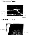
- Figures 6A and 6B are SEM photographs of a semiconductor substrate processed in accordance with the present invention.
- Figure 6A illustrates a cross-sectional side view of a polyimide edge region.
- Figure 6B is a top perspective view of same region.
- Figure 1 illustrates a cross-sectional view of a substrate 20 on which is formed a metal bonding pad 22.
- Bonding pads are commonly used in semiconductor processes to provide a terminal connecting the integrated circuit formed within the silicon substrate, to the external pins of the package.
- Covering bonding pad 22 is a layer of silicon nitride 21.
- Nitride layer 21 encapsulates bonding pad 22 in an insulative layer which prevents electrical shorts from occurring.
- Deposited above nitride layer 21 is a layer of polyamic acid 25. The thickness of layer 25 is typically in the range of 5-6 ⁇ m (50,000-60,000 ⁇ ) thick. Practitioners in the art will appreciate that the processing steps needed to form the substrate of Figure 1 are well understood in the art.
- the substrate is subjected to a curing process.
- the curing process comprises a two-step bake. The first step is performed at approximately 90°C and is for the purpose of removing any solvent which may be present on the substrate surface from previous processing steps. The next step in the curing process is performed at approximately 145°C, a temperature used which is significantly higher than the curing temperature in many prior art processes.
- Figure 5 illustrates a graph showing the etch rate of polyimide in a developer solution versus the cure temperature.
- T C characteristic temperature
- the present invention employs a cure temperature which is significantly higher than the temperature T C .
- point B the etch rate of the polyimide in the developer solution is significantly lower than at point A.
- the etch rate of the polyamic acid layer in the developer solution is approximately 0.1 ⁇ m/second (1000 ⁇ /second). The reason for reducing the etch rate of the polyimide layer will become apparent shortly.
- a layer of photoresist 27 is deposited over the surface of the substrate.
- the photoresist layer is then patterned and exposed to a developer solution which forms opening 29 in the photoresist layer.
- this developing step normally etches the underlying polyamic acid layer all the way down to the nitride layer.
- the etch rate is lowered sufficiently such that the underlying polyamic layer beneath opening 29 is not removed during the developing step. Instead, the developer permeates into the underlying layer to form a salt.
- the developer currently being used comprises a solution of tetramethyl ammonium hydroxide (TMAH) known as NSDTD-2X, which is commercially available through TOK Corporation.
- TMAH tetramethyl ammonium hydroxide
- this developer solution includes a surfactant (the notation "2X" refers to the level of surfactant).
- 2X the level of surfactant
- a number of other commercially available developers may also be used with satisfactory results.
- the net outcome of the developing step is that a salt is formed in region 30 directly beneath opening 29. The remaining regions underneath photoresist masking layer 27 are unchanged during the developing step.
- a hard bake is performed at a sufficiently high temperature so as to imidize the acid regions beneath the photoresist layer 27.
- imidization transforms the polyamic acid into a hard, rigid substance.
- the imidization step is selective; that is, salt region 30 is unchanged while regions 31 are hardened or imidized.
- the hard bake step is performed at approximately 190°C. The temperature of the hard bake controls the etch rate of the polyimide in the subsequent processing step.
- the photoresist layer 27 Is stripped using a solvent.
- the photoresist stripper in current use is known by the name PRS3000, and is commercially available through J.T. Baker Corporation. Resist stripping also develops the exposed polyimide.
- the resulting cross-sectional profile after stripping and developing is shown in Figure 3.
- opening 29 is defined by the edges of polyimide regions 31.
- the edge profile of the polyimide layer exhibits a smooth surface 33 which gradually slopes from the surface of nitride layer 21 to the full thickness of polyimide layer 31.
- Such a graded edge profile is commonly referred to as a "wet etch" profile. This type of profile is extremely desirable when performing sputtering steps.
- sputtering TiW onto the substrate Is a necessary step in the well-known tape automated bonding (i.e., gold bumping) process.
- Figure 4 is a cross-sectional view of the substrate following a vertical etch of nitride layer 21 that exposes the underlying bonding pad 22.
- polyimide layer 31 functions as a masking layer for maintaining the size of opening 29.
- other well-known processing steps may be performed, depending upon the particular semiconductor process utilized. These steps, however, are not essential to the present invention.
- Figures 6A and 6B show photographs taken by a scanning electron microscope (SEM) of an integrated circuit which has been processed in accordance with the present invention.
- Figure 6A is a cross-sectional view showing the wet etch profile produced by the process of the present invention.
- Figure 6B shows a perspective view of the same bonding pad region.
- the polyimide surface is characterized by defect-free, smoothly graded slopes that provide good step coverage for subsequent sputtering steps.
Landscapes
- Internal Circuitry In Semiconductor Integrated Circuit Devices (AREA)
- Formation Of Insulating Films (AREA)
- Wire Bonding (AREA)
Description
Claims (8)
- In a process for fabricating an integrated circuit on a semiconductor substrate, wherein electrical connection to said circuit is made through a plurality of bonding pads disposed on said substrate, a method of protecting said Circuit from mechanical damage comprising the steps of:depositing a layer of polyamic acid over said substrate;baking said substrate at a temperature of approximately 145°C to cure said polyamic acid layer;depositing a layer of photoresist over said acid layer;patterning said photoresist layer;exposing said photoresist layer to said developer to define a plurality of openings therein, said developer permeating into said acid layer in the regions beneath said openings to form a salt therein;imidizing said polyamic acid layer by baking, thereby converting said acid layer to a polyimide layer;removing said photoresist layer and said salt from within said regions, said removing step forming smooth and graded edges on said polyimide layer around said regions.
- The process as defined in claim 1, further comprising the initial step of forming an insulative layer over said bonding pads.
- The process as defined in claim 2 further comprising the final step of etching said insulative layer exposed in said openings.
- The process as defined in claim 3, wherein said insulative layer comprises silicon nitride.
- The process as defined in claim 1, further comprising the additional step, prior to said baking step, of:
a) baking said substrate at a temperature, of approximately 90°C. - The process as defined in claim 5, wherein said developer comprises a base solution.
- The process as defined in claim 6, wherein said developer comprises a solution of tetramethyl ammonium hydroxide which includes a surfactant.
- The process as defined in claim 5, wherein said imidizing step is performed at a temperature of approximately 190°C.
Applications Claiming Priority (2)
| Application Number | Priority Date | Filing Date | Title |
|---|---|---|---|
| US07/893,765 US5242864A (en) | 1992-06-05 | 1992-06-05 | Polyimide process for protecting integrated circuits |
| US893765 | 1992-06-05 |
Publications (2)
| Publication Number | Publication Date |
|---|---|
| EP0573134A1 EP0573134A1 (en) | 1993-12-08 |
| EP0573134B1 true EP0573134B1 (en) | 1998-04-01 |
Family
ID=25402054
Family Applications (1)
| Application Number | Title | Priority Date | Filing Date |
|---|---|---|---|
| EP93300153A Expired - Lifetime EP0573134B1 (en) | 1992-06-05 | 1993-01-11 | Polyimide process for protecting integrated circuits |
Country Status (6)
| Country | Link |
|---|---|
| US (1) | US5242864A (en) |
| EP (1) | EP0573134B1 (en) |
| JP (1) | JP3270909B2 (en) |
| KR (1) | KR100275249B1 (en) |
| DE (1) | DE69317696T2 (en) |
| SG (1) | SG50455A1 (en) |
Families Citing this family (26)
| Publication number | Priority date | Publication date | Assignee | Title |
|---|---|---|---|---|
| US5507903A (en) * | 1991-03-12 | 1996-04-16 | Sumitomo Bakelite Company Limited | Process for producing two-layered tape for tab |
| JP3152796B2 (en) * | 1993-05-28 | 2001-04-03 | 株式会社東芝 | Semiconductor device and method of manufacturing the same |
| US5366589A (en) * | 1993-11-16 | 1994-11-22 | Motorola, Inc. | Bonding pad with circular exposed area and method thereof |
| KR100296174B1 (en) * | 1994-10-14 | 2001-10-24 | 윤종용 | Method of damping vibration and noise of hard disk drive and damping device thereof |
| US6484585B1 (en) | 1995-02-28 | 2002-11-26 | Rosemount Inc. | Pressure sensor for a pressure transmitter |
| US5474956A (en) * | 1995-03-14 | 1995-12-12 | Hughes Aircraft Company | Method of fabricating metallized substrates using an organic etch block layer |
| US6803327B1 (en) | 1999-04-05 | 2004-10-12 | Taiwan Semiconductor Manufacturing Company | Cost effective polymide process to solve passivation extrusion or damage and SOG delminates |
| US6534422B1 (en) * | 1999-06-10 | 2003-03-18 | National Semiconductor Corporation | Integrated ESD protection method and system |
| US6505516B1 (en) | 2000-01-06 | 2003-01-14 | Rosemount Inc. | Capacitive pressure sensing with moving dielectric |
| US6508129B1 (en) | 2000-01-06 | 2003-01-21 | Rosemount Inc. | Pressure sensor capsule with improved isolation |
| US6520020B1 (en) | 2000-01-06 | 2003-02-18 | Rosemount Inc. | Method and apparatus for a direct bonded isolated pressure sensor |
| DE60108217T2 (en) | 2000-01-06 | 2005-12-29 | Rosemount Inc., Eden Prairie | CORN GROWTH METHOD FOR THE PRODUCTION OF AN ELECTRICAL CONNECTION FOR MICROELECTROMECHANICAL SYSTEMS (MEMS) |
| US6561038B2 (en) | 2000-01-06 | 2003-05-13 | Rosemount Inc. | Sensor with fluid isolation barrier |
| US6635585B1 (en) | 2000-10-20 | 2003-10-21 | Aptos Corporation | Method for forming patterned polyimide layer |
| US6774365B2 (en) * | 2001-03-28 | 2004-08-10 | Advanced Micro Devices, Inc. | SEM inspection and analysis of patterned photoresist features |
| US6716571B2 (en) * | 2001-03-28 | 2004-04-06 | Advanced Micro Devices, Inc. | Selective photoresist hardening to facilitate lateral trimming |
| US6815359B2 (en) * | 2001-03-28 | 2004-11-09 | Advanced Micro Devices, Inc. | Process for improving the etch stability of ultra-thin photoresist |
| JP3825314B2 (en) * | 2001-12-17 | 2006-09-27 | 株式会社ルネサステクノロジ | Manufacturing method of semiconductor device |
| US6848316B2 (en) | 2002-05-08 | 2005-02-01 | Rosemount Inc. | Pressure sensor assembly |
| US7030004B2 (en) * | 2003-11-10 | 2006-04-18 | 1St Silicon (Malaysia) Sdn Bhd | Method for forming bond pad openings |
| JP2005235860A (en) * | 2004-02-17 | 2005-09-02 | Sanyo Electric Co Ltd | Semiconductor device and manufacturing method thereof |
| DE102004018468A1 (en) | 2004-04-16 | 2006-02-16 | eupec Europäische Gesellschaft für Leistungshalbleiter mbH | Process for the structured application of a laminatable film to a substrate for a semiconductor module |
| TWI283443B (en) * | 2004-07-16 | 2007-07-01 | Megica Corp | Post-passivation process and process of forming a polymer layer on the chip |
| JP5318055B2 (en) | 2010-09-22 | 2013-10-16 | 株式会社東芝 | Semiconductor device and manufacturing method of semiconductor device |
| US9472515B2 (en) * | 2014-03-11 | 2016-10-18 | Intel Corporation | Integrated circuit package |
| US10636696B1 (en) * | 2019-01-18 | 2020-04-28 | Applied Materials, Inc. | Methods for forming vias in polymer layers |
Family Cites Families (11)
| Publication number | Priority date | Publication date | Assignee | Title |
|---|---|---|---|---|
| US4369090A (en) * | 1980-11-06 | 1983-01-18 | Texas Instruments Incorporated | Process for etching sloped vias in polyimide insulators |
| US4411735A (en) * | 1982-05-06 | 1983-10-25 | National Semiconductor Corporation | Polymeric insulation layer etching process and composition |
| JPS601846A (en) * | 1983-06-18 | 1985-01-08 | Toshiba Corp | Multilayer interconnection structure semiconductor device and manufacture thereof |
| US4606998A (en) * | 1985-04-30 | 1986-08-19 | International Business Machines Corporation | Barrierless high-temperature lift-off process |
| EP0224680B1 (en) * | 1985-12-05 | 1992-01-15 | International Business Machines Corporation | Diazoquinone sensitized polyamic acid based photoresist compositions having reduced dissolution rates in alkaline developers |
| US4830706A (en) * | 1986-10-06 | 1989-05-16 | International Business Machines Corporation | Method of making sloped vias |
| US4827326A (en) * | 1987-11-02 | 1989-05-02 | Motorola, Inc. | Integrated circuit having polyimide/metal passivation layer and method of manufacture using metal lift-off |
| US4846929A (en) * | 1988-07-13 | 1989-07-11 | Ibm Corporation | Wet etching of thermally or chemically cured polyimide |
| US4857143A (en) * | 1988-12-16 | 1989-08-15 | International Business Machines Corp. | Wet etching of cured polyimide |
| US5019535A (en) * | 1989-03-28 | 1991-05-28 | General Electric Company | Die attachment method using nonconductive adhesive for use in high density interconnected assemblies |
| US5133840A (en) * | 1990-05-15 | 1992-07-28 | International Business Machines Corporation | Surface midification of a polyimide |
-
1992
- 1992-06-05 US US07/893,765 patent/US5242864A/en not_active Expired - Lifetime
-
1993
- 1993-01-11 SG SG1996001823A patent/SG50455A1/en unknown
- 1993-01-11 DE DE69317696T patent/DE69317696T2/en not_active Expired - Lifetime
- 1993-01-11 EP EP93300153A patent/EP0573134B1/en not_active Expired - Lifetime
- 1993-01-12 KR KR1019930000298A patent/KR100275249B1/en not_active Expired - Fee Related
- 1993-06-07 JP JP16004193A patent/JP3270909B2/en not_active Expired - Fee Related
Also Published As
| Publication number | Publication date |
|---|---|
| DE69317696D1 (en) | 1998-05-07 |
| US5242864A (en) | 1993-09-07 |
| KR100275249B1 (en) | 2001-01-15 |
| JPH06204280A (en) | 1994-07-22 |
| JP3270909B2 (en) | 2002-04-02 |
| DE69317696T2 (en) | 1998-11-05 |
| KR940001382A (en) | 1994-01-11 |
| SG50455A1 (en) | 1998-07-20 |
| EP0573134A1 (en) | 1993-12-08 |
Similar Documents
| Publication | Publication Date | Title |
|---|---|---|
| US5242864A (en) | Polyimide process for protecting integrated circuits | |
| EP0100735B1 (en) | Lift-off process for fabricating self-aligned contacts | |
| US4076575A (en) | Integrated fabrication method of forming connectors through insulative layers | |
| US5162257A (en) | Solder bump fabrication method | |
| CA1223089A (en) | Barrierless high-temperature lift-off process | |
| JPH06196399A (en) | Method for formation of patterned film on substrate | |
| CN100492625C (en) | Electronic component and method for manufacturing the same | |
| US5705432A (en) | Process for providing clean lift-off of sputtered thin film layers | |
| JPH01315163A (en) | Manufacture of semiconductor integrated circuit device | |
| US6878642B1 (en) | Method to improve passivation openings by reflow of photoresist to eliminate tape residue | |
| JP2842405B2 (en) | Method for manufacturing semiconductor device | |
| US6320269B1 (en) | Method for preparing a semiconductor wafer to receive a protective tape | |
| JP2808674B2 (en) | Method for manufacturing semiconductor device | |
| US6071824A (en) | Method and system for patterning to enhance performance of a metal layer of a semiconductor device | |
| KR100220796B1 (en) | Method for making bump area | |
| JPH06177136A (en) | Circuit device with bump electrodes | |
| JP2991388B2 (en) | Method for manufacturing semiconductor device | |
| JPH10189583A (en) | Semiconductor device | |
| US7071101B1 (en) | Sacrificial TiN arc layer for increased pad etch throughput | |
| JP3109506B2 (en) | Pattern formation method | |
| KR0161871B1 (en) | Metal wire manufacturing method of semiconductor device | |
| JPH08107112A (en) | Wiring forming method for semiconductor device | |
| JP2000269326A (en) | Method for manufacturing semiconductor device | |
| JP2570709B2 (en) | Etching method | |
| KR0169761B1 (en) | Metal wiring forming method of semiconductor device |
Legal Events
| Date | Code | Title | Description |
|---|---|---|---|
| PUAI | Public reference made under article 153(3) epc to a published international application that has entered the european phase |
Free format text: ORIGINAL CODE: 0009012 |
|
| AK | Designated contracting states |
Kind code of ref document: A1 Designated state(s): CH DE FR GB LI |
|
| 17P | Request for examination filed |
Effective date: 19940527 |
|
| 17Q | First examination report despatched |
Effective date: 19950809 |
|
| GRAG | Despatch of communication of intention to grant |
Free format text: ORIGINAL CODE: EPIDOS AGRA |
|
| GRAG | Despatch of communication of intention to grant |
Free format text: ORIGINAL CODE: EPIDOS AGRA |
|
| GRAH | Despatch of communication of intention to grant a patent |
Free format text: ORIGINAL CODE: EPIDOS IGRA |
|
| GRAH | Despatch of communication of intention to grant a patent |
Free format text: ORIGINAL CODE: EPIDOS IGRA |
|
| GRAA | (expected) grant |
Free format text: ORIGINAL CODE: 0009210 |
|
| AK | Designated contracting states |
Kind code of ref document: B1 Designated state(s): CH DE FR GB LI |
|
| REG | Reference to a national code |
Ref country code: CH Ref legal event code: EP |
|
| REG | Reference to a national code |
Ref country code: CH Ref legal event code: NV Representative=s name: AMMANN PATENTANWAELTE AG BERN |
|
| REF | Corresponds to: |
Ref document number: 69317696 Country of ref document: DE Date of ref document: 19980507 |
|
| ET | Fr: translation filed | ||
| PLBE | No opposition filed within time limit |
Free format text: ORIGINAL CODE: 0009261 |
|
| 26N | No opposition filed | ||
| REG | Reference to a national code |
Ref country code: GB Ref legal event code: IF02 |
|
| PGFP | Annual fee paid to national office [announced via postgrant information from national office to epo] |
Ref country code: CH Payment date: 20100125 Year of fee payment: 18 |
|
| PGFP | Annual fee paid to national office [announced via postgrant information from national office to epo] |
Ref country code: FR Payment date: 20100205 Year of fee payment: 18 |
|
| PGFP | Annual fee paid to national office [announced via postgrant information from national office to epo] |
Ref country code: GB Payment date: 20100125 Year of fee payment: 18 Ref country code: DE Payment date: 20100127 Year of fee payment: 18 |
|
| REG | Reference to a national code |
Ref country code: CH Ref legal event code: PL |
|
| GBPC | Gb: european patent ceased through non-payment of renewal fee |
Effective date: 20110111 |
|
| REG | Reference to a national code |
Ref country code: FR Ref legal event code: ST Effective date: 20110930 |
|
| PG25 | Lapsed in a contracting state [announced via postgrant information from national office to epo] |
Ref country code: CH Free format text: LAPSE BECAUSE OF NON-PAYMENT OF DUE FEES Effective date: 20110131 Ref country code: LI Free format text: LAPSE BECAUSE OF NON-PAYMENT OF DUE FEES Effective date: 20110131 Ref country code: FR Free format text: LAPSE BECAUSE OF NON-PAYMENT OF DUE FEES Effective date: 20110131 |
|
| PG25 | Lapsed in a contracting state [announced via postgrant information from national office to epo] |
Ref country code: GB Free format text: LAPSE BECAUSE OF NON-PAYMENT OF DUE FEES Effective date: 20110111 |
|
| REG | Reference to a national code |
Ref country code: DE Ref legal event code: R119 Ref document number: 69317696 Country of ref document: DE Effective date: 20110802 |
|
| PG25 | Lapsed in a contracting state [announced via postgrant information from national office to epo] |
Ref country code: DE Free format text: LAPSE BECAUSE OF NON-PAYMENT OF DUE FEES Effective date: 20110802 |