EP0570158B1 - Frequency multiplication circuit and method for generating a stable clock signal - Google Patents
Frequency multiplication circuit and method for generating a stable clock signal Download PDFInfo
- Publication number
- EP0570158B1 EP0570158B1 EP19930303528 EP93303528A EP0570158B1 EP 0570158 B1 EP0570158 B1 EP 0570158B1 EP 19930303528 EP19930303528 EP 19930303528 EP 93303528 A EP93303528 A EP 93303528A EP 0570158 B1 EP0570158 B1 EP 0570158B1
- Authority
- EP
- European Patent Office
- Prior art keywords
- input
- output
- clock signal
- delay
- clock
- Prior art date
- Legal status (The legal status is an assumption and is not a legal conclusion. Google has not performed a legal analysis and makes no representation as to the accuracy of the status listed.)
- Expired - Lifetime
Links
Images


Classifications
-
- G—PHYSICS
- G06—COMPUTING OR CALCULATING; COUNTING
- G06F—ELECTRIC DIGITAL DATA PROCESSING
- G06F1/00—Details not covered by groups G06F3/00 - G06F13/00 and G06F21/00
- G06F1/04—Generating or distributing clock signals or signals derived directly therefrom
- G06F1/10—Distribution of clock signals, e.g. skew
-
- H—ELECTRICITY
- H03—ELECTRONIC CIRCUITRY
- H03K—PULSE TECHNIQUE
- H03K5/00—Manipulating of pulses not covered by one of the other main groups of this subclass
- H03K5/00006—Changing the frequency
-
- H—ELECTRICITY
- H03—ELECTRONIC CIRCUITRY
- H03K—PULSE TECHNIQUE
- H03K5/00—Manipulating of pulses not covered by one of the other main groups of this subclass
- H03K5/15—Arrangements in which pulses are delivered at different times at several outputs, i.e. pulse distributors
- H03K5/15013—Arrangements in which pulses are delivered at different times at several outputs, i.e. pulse distributors with more than two outputs
- H03K5/15026—Arrangements in which pulses are delivered at different times at several outputs, i.e. pulse distributors with more than two outputs with asynchronously driven series connected output stages
Definitions
- This invention relates to the generation of clock signals, and more particularly is directed to internal clock generation and distribution schemes in integrated circuits.
- Clock signals may be generated in systems using these circuits by way of a stand-alone crystal oscillator circuit, or by connection of a crystal to terminals of the clocked logic device itself in the case where the oscillator is integrated onto the same integrated circuit chip with the logic function.
- the rate at which a clocked integrated circuit performs its function is generally highly dependent upon the frequency of the clock signal. Especially in digital circuits, this is because the internal chip functions are either directly or indirectly (via frequency dividers, phase-locked loops and the like) controlled by the received clock signal. As such, for the example of a microprocessor, the number of instructions performable by the circuit in a given period of time will vary with the frequency of the clock signal.
- the performance of certain circuit functions may depend on the clock frequency while the rate at which other functions are performed may be limited by other factors.
- certain input-output functions may be limited by bus interface specifications rather than the clock frequency, while the speed of core or CPU functions will likely depend directly on the clock frequency.
- clock doubling particularly in the case where the core clock is operating at twice the rate of the bus interface clocks.
- a conventional circuit for deriving clock signals at various frequencies from an input clock signal is the combination of a phase-locked loop (PLL) and one or more frequency dividers.
- the PLL provides stability in the generated output clock signals relative to the input clock, while the ratio of the frequency dividers in the output and feedback loops determines the relative frequency between the output clock signals and the input clock.
- a PLL circuit cannot instantaneously respond to a change in the input clock frequency, as several transition cycles may be necessary to lock onto a new input clock signal frequency.
- PLL-based circuits are generally limited in operating power supply voltage range (primarily due to the operation of the voltage controlled oscillator), and as such are not well-suited for use in circuits that are to operate over a wide power supply voltage range.
- lower power supply voltages e.g., 3.3 volts
- Another known technique for providing different clock frequencies to different circuit portions is to have two terminals for receiving input clocks at different frequencies.
- the state of another terminal (either hardwired externally or connected in the wiring of an on-chip bond pad) selects whether the clock signal received at the alternate clock terminal is to be ignored or used.
- Certain other clock doubling schemes have considered the use of internal frequency dividers to divide down the input clock frequency prior to application to slower circuit functions. For example, it is known to use a half-frequency clock (relative to the input clock frequency) to control the bus interface of a microprocessor circuit. In such arrangements, the frequency divider not only reduces the clock frequency, but also corrects for variations in duty cycle and ringing conditions on the input clock signal. While such correction for input clock instabilities may be performed prior to use in slower circuit functions, these instabilities preclude the direct use of the input clock signal for the high speed circuit functions in the CPU or core. In particular, certain phases of the input clock signal may be too short (especially when unstable) to allow for completion of certain internal core functions.
- integrated circuits are conventionally manufactured, beginning with wafer fabrication, to be of the clock doubled type or of the non-clock doubled type, with the quantity manufactured of each type determined according to customer demand.
- the cost of maintaining manufacturing inventory is made more difficult, however, as the number of circuit types increases, especially if circuit demand or manufacturing yield is subject to fluctuation. Accordingly, it is desirable to provide an integrated circuit having both clock doubling and non-clock doubling capability.
- a control signal selects which of multiple clock signals is to control the operation of certain integrated circuit functions (such as the core unit and the bus interface unit).
- the selection of which of a plurality of clocks that a particular circuit is to respond required relatively complex circuitry to implement this ability to respond to a selected clock signal. Since such circuitry loads and otherwise affects the path of the clock used to control the speed of the circuit function, such selection circuitry necessarily affects the most critical timing path of the circuits.
- US-A-4217639 discloses a logic circuit that generates two clock pulses at the output of an exclusive-OR gate during a single clock cycle initiated by the presence of a binary 1 level at an input of a NAND gate having an output feeding a delay.
- the exclusive-OR gate receives inputs from a tap on and the output from the delay which also provides a feedback input to the NAND gate.
- a binary 0 level is established at a third input of the NAND gate by a flip-flop to inhibit operation after the second clock pulse has been output from the exclusive-OR gate.
- clock generating circuitry for generating output clock signals (CORECLK) responsive to an input clock signal (CLKIN), comprising: a resettable latch circuit for generating a sequence of output clock signal edges in response to the occurrence of a single active edge of said input clock signal; said latch circuit including a first input (S) coupled to receive a signal input from detection circuitry in response to detection of said active edge of the input clock signal thereby causing a first output transition in a first direction of said latch circuit; said latch output being coupled by a delay means and a first active edge detector to another input (R) of the latch circuit to apply a signal input to said another input causing a latch output transition in an opposite direction from said first direction in response to detection of an output transition in the first direction after a predetermined delay provided by said delay means; circuitry including a delay means coupled to a second active edge detector to detect delayed output transitions of said latch circuit in a predetermined direction and in response to each detected transition to apply a further input to said first input
- a method of generating output clock signals (CORECLK) responsive to an input clock signal (CLKIN) by initiating a sequence comprising: operating a resettable latch circuit to generate a series of output clock signal edges in response to the occurrence of a single active edge of said input clock signal; applying a signal input to a first input (S) of said latch circuit in response to detection of said active edge of the input clock signal thereby causing a first output transition of said latch circuit in a first direction; after a predetermined delay causing a latch circuit output transition in an opposite direction from said first direction in response to detection by a first active edge detector of an output transition in the first direction, by applying a signal input to another input (R) of said latch circuit; and then in response to detection by a second active edge detector of an output transition of said latch circuit in a predetermined direction, applying a further input to said first input of the latch circuit after a predetermined delay to cause another output transition of said latch circuit in the first direction, to initiate repetition of said
- the clock generator circuitry includes a delay which may be selected according to the worst case delay path for one of the clock phases; this delay period determines the duty cycle of the generated output clock signal independent of the input clock signal duty cycle.
- the delay period is generated by a delay stage having a fixed portion and a variable portion; the fixed portion includes gate delays of various types so that process, voltage and temperature variations in an integrated circuit and its operation are matched by changes in the delay stages.
- the variable portion of the delay stage facilitates characterization and adjustment of the delay period.
- integrated circuit 2 such as a microprocessor, math co-processor or the like having at least two different functions which can operate at different clock frequencies, and thus in which the preferred embodiment of the invention is implemented will be described.
- integrated circuit 2 includes a core unit 4 which performs a sequence of instructions or some other complex logic operation, preferably at the fastest possible clock frequency to optimize circuit performance.
- Integrated circuit 2 further includes bus interface unit 6 which is in communication with input and output terminals (not shown) of integrated circuit 2, and is also in communication with core unit 4 by way of internal bus IBUS.
- Bus interface unit 6 is intended to receive input signals presented at address and data input terminals, to control the operation of core unit 4 and other functions in integrated circuit 2, and also to control the presentation of output data at output terminals; since the timing requirements of bus interface unit 6 are governed by the input/output specifications of other integrated circuits in the system, it may require a slower clock frequency than that usable by core unit 4.
- FIG. 1 For reference hereinbelow, certain of the input terminals to integrated circuit 2 are illustrated in Figure 1 as being connected to circuitry via a bond wire W and a bond pad BP. Other inputs and outputs are, of course, similarly connected but are not shown in Figure 1 for purposes of clarity.
- the illustration of the bond pads BP in Figure 1 will become apparent relative to the optional wire bonding of one of the bond pads BP discussed hereinbelow.
- conventional input buffer circuits may also be provided within integrated circuit 2 in the conventional manner; such buffers are also not illustrated in Figure 1 for purposes of clarity.
- integrated circuit 2 is operable to receive an input clock signal at terminal CLKIN.
- the input clock signal may be an externally generated periodic clock, such as from an external oscillator, or alternatively the input clock signal may be generated on-chip based on a crystal connected to terminal CLKIN that determines the clock frequency.
- Clock control circuit 8 presents to core unit 4 (on line CORECLK) an internal clock signal at the same frequency as the input clock signal at terminal CLKIN, and presents to bus interface unit 6 (on line BUSCLK) an internal clock signal at one-half the frequency of the input clock signal received at terminal CLKIN.
- the half-frequency clock signal is generated and applied to line BUSCLK by frequency divider 10, which in this case divides the input clock signal frequency by two prior to its presentation on line BUSCLK.
- clock control circuit 8 further includes clock generator 12 which receives the input clock signal from terminal CLKIN at a "set” input, and which receives the input clock signal from terminal CLKIN, delayed by programmable delay stage 14, at a "reset” input.
- Programmable delay stage 14 in this arrangement includes a default delay value that is enabled for normal (non-test mode) operation, implemented within programmable delay stage 14 by the metallization pattern or by way of fusible links or other programmable elements (FAMOS transistors, etc.).
- programmable delay stage 14 also receives a test input from terminal TEST and j select lines 15 j from selected input terminals IN 0 through IN n so that, in a special test mode selected by the logic state applied to terminal TEST, the j select lines 15 j can select a portion of the delay period through delay stage 14.
- Programmable delay stage 14 and clock generator 12 each also receive an input on line 2XEN indicating if the clock doubling mode is to be enabled; when enabled, the clock doubling mode causes the core unit clock frequency on line CORECLK to be twice that of the bus clock frequency on line BUSCLK.
- selection of the clock doubling feature is made at the wire bonding step of the manufacturing process, by connecting the bond pad BP associated with line 2XEN to be connected to the V cc power supply terminal (which, in this example, enables clock doubling) or to the V ss or ground terminal (disabling clock doubling).
- clock control circuit 8 is controlled by the state of line 2XEN, so that the clock signal on line CORECLK may be generated either in a clock doubling mode or in a non-clock doubling mode.
- interface circuitry controlling the communication of data on internal bus IBUS is also preferably controlled according to the state of line 2XEN, so that communication between core unit 4 and bus interface unit 6 can be performed according to the selected internal clock relationship. It is contemplated that the construction of such interface circuitry will be apparent to one of ordinary skill in the art having reference to this specification.
- clock generator 12 operates in the clock doubling mode to respond to one of the input clock signal edges; for purposes of this description, the term “rising edge” will refer to a low-to-high transition for a signal, and the term “falling edge” will refer to a high-to-low transition.
- the rising edge of the input clock signal sets the output of clock generator 12 (on line CORECLK) to a high level.
- Clock generator 12 resets low its output on line CORECLK responsive to receiving the rising edge of the input clock signal, delayed by the time delay set within programmable delay stage 14.
- the delay period of programmable delay stage 14 is preferably selected to slightly exceed the time required for the worst case clock phase in the instruction set or possible operations of core unit 4.
- clock generator 12 uses edge triggered set and reset functions based on the input clock signal, and provides an internal clock signal on line CORECLK that is at the same frequency as the input clock signal at terminal CLKIN, at a fixed phase duration so that variations in the duty cycle of the input clock signal thus do not affect the duty cycle of the internal clock signal on line CORECLK.
- the delay period is preferably selected according to the propagation delay of the worst case logic path, thus ensuring proper operation of integrated circuit 2 regardless of the duty cycle of the input clock signal, and thus over a wide range of duty cycle timing specifications.
- frequency divider 10 is generating a clock signal on line BUSCLK that is at half the frequency of the input clock signal at terminal CLKIN. Accordingly, the operation of bus interface unit 6 can be controlled in a manner consistent with externally connected integrated circuits, while still allowing the operation of core unit 4 to perform at the highest practicable clock rate.
- Frequency divider 10 in this example is of substantially conventional design, and includes a reset function by which its output may be suspended.
- Line CLKIN communicates the input clock signal (after buffering if desired) to inverters 13 and 17, which generate complement and true clock signals on lines CLKc and CLKt, respectively.
- Each of pass gates 24, 26 consist of complementary MOS transistors having their source/drain paths connected in parallel with one another, and having their gates connected to complementary lines CLKt, CLKc so as to be simultaneously on or off.
- Line RST communicates a reset signal from elsewhere in integrated circuit 2 to an input of NAND gate 22 in frequency divider 10 and to start/stop logic 30 in clock generator 12.
- Line RST is preferably buffered within integrated circuit 2, in the conventional manner, to eliminate false resets due to noise, and to ensure proper phase synchronisation after reset.
- the second input of NAND gate 22 is connected to the output of frequency divider 10 on line BUSCLK.
- the low logic level on line RST presents a high logic level (via inverter 21) to one input of NAND gate 22, allowing the state of line BUSCLK to control the output of NAND gate 22.
- the output of NAND gate 22 is connected to one side of pass gate 24.
- the other side of pass gate 24 is received by latch 28 and communicated to one side of pass gate 26 (after inversion by inverter 27 to account for the inversion by latch 28).
- Latch 28, in this example and elsewhere, consists of a pair of cross-coupled inverters where the feedback inverter has significantly weaker drive than the feed-forward inverter so that it can be rapidly overwritten as a new logic level is received at its input; this weaker drive is illustrated in Figure 2 by an asterisk in the feedback inverter of latch 28 (and in other latches in Figures 2 and 3).
- pass gate 24 is operable to pass the state of the output of NAND 22 to latch 28 during the low level phase of the input clock signal on line CLKIN. Accordingly, if line RST is low during this phase, the logical complement of the state of line BUSCLK is communicated to latch 28 during low phases of the input clock signal. After inversion by inverter 27, the state of latch 28 is communicated to pass gate 26.
- Pass gate 26 has its other side connected to latch 20 which, via inverter 19, drives line BUSCLK.
- pass gate 26 has its gates controlled by lines CLKt, CLKc in a complementary manner relative to pass gate 24, such that pass gate 26 is conductive during high level phases of the input clock signal at line CLKIN. Accordingly, the complement of the state of line BUSCLK thus requires both a low level phase and a high level phase to be communicated back to latch 20, for presentation (after inversion by inverter 19) on line BUSCLK as a logic level transition of this output clock. As such, the frequency at which line BUSCLK toggles will be exactly one-half that of the input clock signal at line CLKIN.
- NAND gate 22 is operable to respond to the state of line BUSCLK; conversely, in a reset or suspend operation, where line RST is at a high logic level, the output of NAND gate 22 is forced high regardless of the state of line BUSCLK. Accordingly, the state of line BUSCLK is held high during the reset condition.
- Start/stop logic receives line RST (via inverter 21), line BUSCLK, and start and stop signals on lines STRT and STP, respectively.
- Start/stop logic 30 includes such combinational logic as required to enable and disable clock generator 12 according to the reset condition on line RST, and according to the start and stop signals.
- the start and stop signals allow for suspension of the output clock signal on line CORECLK, as will be described hereinbelow.
- the input clock signal at line CLKIN is communicated to an inverting input of NAND gate 34 and to a non-inverting input of NAND gate 36.
- the second input of NAND gate 34 receives line 2XEN which enables clock doubling with a high logic level.
- the output of NAND gate 34 is communicated, via inverting delay stage 35, to the second input of NAND gate 36.
- Delay stage 35 may consist of several inverters in series, of a conventional single delay stage, or other conventional delay circuits for delaying the propagation of the signal from the output of NAND gate 34 to the input of NAND gate 36 for a selected time.
- NAND gate 36 will present a low logic level pulse responsive to the rising edge of the input clock signal at line CLKIN, and having a pulse width corresponding to the propagation delay of NAND gate 34 and delay stage 35.
- the output of NAND gate 36 is connected to the gate of a p-channel transistor 38 having its source-drain path connected between V cc and the input of latch 40; the output of latch 40 drives line CORECLK via inverter 41.
- variable delay stage 14v receives inputs on line TEST and on j select lines 15j, as shown in Figure 1.
- the output of variable delay stage 14v on line CLKDELAY is connected to a non-inverting input of NAND gate 46 and to an inverting input of NAND gate 44.
- the second input of NAND gate 44 receives line 2XEN.
- the output of NAND gate 44 is connected to a second input of NAND gate 46 via inverting delay stage 45.
- NAND gate 46 will present a low logic level pulse responsive to the rising edge of the signal on line CLKDELAY from variable delay stage 14v, having a pulse width defined by the delay through NAND gate 44 and delay stage 45.
- the output of NAND gate 46 is connected, after inversion by inverter 47, to the gate of an n-channel transistor 42 having its source/drain path connected between the input of latch 40 and ground.
- NAND gate 46 also receives an input from the output of start/stop logic 30, thus allowing the reset signal on line RST, and the start and stop signals on lines STRT and STP, to control the operation of clock generator 12 in the clock doubling mode. For example, if start/stop logic 30 drives a low logic level at its output, the output of NAND gate 46 will be forced high, ensuring that n-channel transistor 42 does not turn on. In such an event, latch 40 cannot be overwritten with a low level, thus disabling transitions of the clock signal on line CORECLK.
- Line 2XEN is also connected to an inverting input of NAND gate 50, which receives the input clock signal on line CLKIN at its other input.
- the output of NAND gate 50 is connected to pass gate 48 in complementary fashion (via inverter 49); as such, pass gate 48 is made non-conductive when line 2XEN is high, during the clock doubling mode.
- Clock generator 12 also can provide a half-frequency clock signal on line CORECLK during the non-clock doubling mode indicated by line 2XEN being at a low logic level.
- NAND gate 32 receives the output of latch 28 in frequency divider 10 at one input, and receives the output of start/stop logic 30 at the other input.
- Start/stop logic 30 is therefore able to gate the application of the output of latch 28 to the frequency divider portion of clock generator 12, such as is useful in suspending its operation (as in the case of line RST being high for frequency divider 10) and restarting it in a synchronous manner.
- NAND gate 32 The output of NAND gate 32 is presented to one side of pass gate 48.
- the opposite side of pass gate 48 is coupled to the input of latch 40.
- the n-channel transistor in pass gate 48 receives a signal corresponding to the input clock signal on line CLKIN
- the p-channel transistor in pass gate 48 receives a signal corresponding to the logical complement of the input clock signal on line CLKIN; as such, pass gate 48 is gated similarly as pass gate 26 in frequency divider 10.
- clock generator 12 is configured similarly as frequency divider 10 (with the two circuits sharing the first portion thereof of NAND gate 22, pass gate 24 and latch 28), for generating a half-frequency clock on line CORECLK. In this mode, therefore, the frequency of the clock signal on lines CORECLK and BUSCLK are identical.
- Figure 4a illustrates the operation of clock generator 12 in clock doubling mode, selected by line 2XEN being at a high logic level. For purposes of clarity of description, small propagation delays and charging transients are not shown in Figure 4a.
- a rising edge on line CLKIN first causes the output of NAND gate 36 (node S in Figure 4a) to go to a low logic level.
- This low logic level at the output of NAND gate 36 continues until the rising edge propagates through NAND gate 34 and delay stage 35; this propagation delay is shown in Figure 4a as ⁇ 35 , and defines the pulse width of the low logic level at node S.
- transistor 38 turns on, charging the input of latch 40 high which, via inverter 41, drives line CORECLK high. Accordingly, in clock doubling mode the rising edge of the input clock signal operates to set the output of clock generator circuit 12 on line CORECLK.
- the rising edge of the input clock signal at line CLKIN also propagates through delay stages 14f, 14v, appearing at line CLKDELAY after the delay period ⁇ 14 (i.e., the propagation delay through delay stages 14f, 14v).
- the output of NAND gate 46 goes to a low logic level (the other inputs to NAND gate 46 being high).
- the low logic level at the output of NAND gate 46 via inverter 47, drives the gate of n-channel transistor 42 (node R of Figures 2 and 4a) high, turning on transistor 42 and discharging the input of latch 40 to ground.
- Latch 40 and inverter 41 drive line CORECLK low in response to transistor 42 being turned on. Accordingly, the rising edge of the signal on line CLKDELAY operates to reset the output of clock generator 12 on line CORECLK to a low level, delayed from the high level transition by the delay time ⁇ 14 of programmable delay stage 14.
- the duration of the pulse width of the low logic level pulse at node S i.e,. the time delay ⁇ 35
- the duration of the high logic level pulse at node R i.e., the time delay ⁇ 45
- these delays should also be selected to prevent the set and reset pulses from overlapping, as such would cause a crowbar condition (i.e., direct short from V cc to ground) through transistors 38 and 42.
- a clock signal is generated on line CORECLK which is at the same frequency as the input clock signal, but which has a duty cycle independent from that of the input clock signal.
- the duration of one of the phases of the clock on line CORECLK is dependent upon the time between the set and reset pulses (at low and high levels, respectively, in this example).
- the time between the set and reset pulses depends solely upon the delay period ⁇ 14 through programmable delay 14 (i.e., through delay stages 14f, 14v), and does not depend upon the duty cycle of the input clock signal on line CLKIN.
- the duration of the high level phase on line CORECLK is greater than that of the input clock signal on line CLKIN. As will be discussed in further detail hereinbelow, this allows the duty cycle of the internal high frequency clock on line CORECLK to be optimized for the worst case phase, rather than for an average which is dependent upon the input clock signal.
- clock generator 12 thus provides a high degree of stability in the generation of a high frequency internal clock based on a received high frequency input clock signal. Particularly as microprocessor clock frequencies increase to 25 MHz and beyond, the generation and presentation of external clock signals of high quality and stability becomes more difficult, especially considering ringing and other noise effects which become more pronounced with higher switching speeds. Since clock generator 12 generates its clock signals based on edges of the input clock signal, and on internal delays, the clock signal on line CORECLK is not strongly affected by noise and other instabilities in the input clock signal.
- This low logic level is also communicated via NAND gate 32 (the output of start/stop logic 30 being high to enable operation) as a low level (inverted twice by latch 28 and NAND gate 32) to node IN48 at the input to pass gate 48.
- Pass gates 26 and 48 are non-conductive during this phase of the input clock signal, as they are gated in a complementary fashion relative to pass gate 24.
- pass gates 26 and 48 Upon the rising edge of the input clock signal, pass gates 26 and 48 become conductive and pass gate 24 turns off. Latch 28 retains its low logic level input at this time due to the operation of its feedback inverter. With pass gate 26 conductive, the state of node IN28 is communicated (after inversion by latch 28 and by inverter 27) to node IN20 at the input of latch 20, thus presenting a low logic level on line BUSCLK. Similarly, with pass gate 48 conductive, the low logic level at node IN48 is communicated to the input of latch 40 (node IN40), and presented on line CORECLK.
- inverter 27 may be replaced by a series of inverters, with propagation delay there through as desired.
- clock generator 12 may be readily configured to provide a complementary clock signal to the signal on line CORECLK, for example by providing a similar circuit to that of latch 40 and transistors 38, 42, 48, but which operates in complementary fashion. It is contemplated that other clock signals may be generated from those signals shown in Figure 2 by the addition of such elementary logic as would be known by one of ordinary skill in the art having reference to this description.
- clock control circuit 8 provides significant advantages in the design and operation of integrated circuit 2 over prior techniques.
- clock control circuit 8 to generate output clock signals in a selected mode allows the functional circuitry, such as core unit 4, to be designed so that it need only respond to a single internal clock signal, as the determination of the core clock frequency is made by clock control circuit 8.
- the selection of which clock mode is made in this example, by the bonding of pad 2XEN to a power supply or ground pad.
- This method of selecting the clock mode is especially beneficial to the manufacturer, as only a single type of integrated circuit 2 need be fabricated in order to provide inventory for both types of products (clock doubled or not), as the selection of the operation mode need not be made at the initial wafer fabrication stage, but instead is determined in the packaging operation.
- the user of integrated circuit 2 is not required to make any provision, such as externally connecting a terminal high or low, in order to maintain the proper desired operating mode.
- clock generator 12 thus generates an internal clock signal having a duty cycle which depends upon a delay time ⁇ 14 through programmable delay stage 14.
- one of the two clock phases will control the worst case logic propagation path, such that the duration of the worst case phase will be critical in the operation of the circuit (i.e., if the duration of this worst case clock phase is too short, the circuit will malfunction).
- programmable delay stage 14 preferably includes a fixed delay stage 14f and a variable delay stage 14v, such that the delay time ⁇ 14 , and thus the duration of the worst case clock phase, may be set or altered either during characterization, production test or in operation.
- the ratio t d /t h remain substantially constant over voltage, temperature, and processing conditions.
- V cc power supply voltage i.e., nominally 5 volts
- V cc levels i.e., nominally 3.3 volts
- This construction of programmable delay stage 14 includes such features as to provide a delay time ⁇ 14 that matches variations in voltage, temperature and processing which affect the minimum clock phase duration time t h , and to provide the ability to readily change the delay time ⁇ 14 as necessary.
- Fixed delay stage 14f receives the input clock signal on line CLKIN via pass gate 59, controlled in complementary fashion by the signal on line 2XEN. In non-clock doubling mode (since the clock signal on line CLKDELAY is not used; see Figures 3 and 4b) with line 2XEN low, pass gate 59 is non-conductive; during clock doubling mode, pass gate 59 remains conductive.
- Fixed delay stage 14f includes multiple delay elements of various logic types, selected according to the worst case propagation delay in core unit 4 or elsewhere in circuit 2.
- fixed delay stage 14f includes latch 52, inverter 53, NOR gate 54 (with another input tied to ground), three-input NAND gate 55 (with its two other inputs tied high), two-input NAND gate 56 (with its other input tied high), pass gate 57 (biased on), and capacitors 58a, 58b biased to V cc and ground, respectively.
- Capacitors 58a, 58b represent parasitic capacitances in core unit 4, and may be implemented as separate capacitors in fixed delay stage 14f, or by way of parasitic capacitances therein. While one of each type of delay element is illustrated in Figure 3, fixed delay stage 14f may include multiple ones of these elements, multiple chains of elements, or such other elements and combinations as useful to mimic the worst case core unit 4 delay path.
- Variable delay stage 14v receives the output of fixed delay stage 14f, and adds a selectable amount of delay thereto, prior to presenting the result at its output on line CLKDELAY.
- Variable delay stage 14v in this preferred construction can select various delays in a special test mode, with a default delay set by way of metal mask options.
- the selection of the delay through variable delay stage 14v may be made in substantially equal increments by a binary code, thus allowing great flexibility in the selection of the overall delay time ⁇ 14 .
- variable delay stage 14v includes four individually selectable delay paths.
- the most significant delay path is a set of four inverter pairs 60 selectable by multiplexer 64 3 .
- the next most significant delay path has two inverter pairs 60 selectable by multiplexer 64 2 ; with the next most significant delay path having one inverter pair 60 selectable by multiplexer 64 1 .
- Each of the inverter pairs 60 preferably has the same propagation delay there through (i.e., delay ⁇ ').
- the least significant delay path is implemented by the connection of capacitor 61 by pass gate 62, adding a capacitive load which preferably matches one-half the delay ⁇ ' of an inverter pair 60, or the propagation delay of a single inverter. Accordingly, the delay time through variable delay stage 14v may be selected in a binary fashion, as the four selectable paths are weighted in a binary fashion (2 3 , 2 2 , 2 1 , and 2 0 inverters, respectively).
- Multiplexers 64 cause the series path of the clock signal from fixed delay stage 14f to either pass through associated delay elements, or pass directly to the next stage without being delayed, responsive to the control input applied thereto from multiplexers 70 3 through 70 0 , respectively.
- Each of multiplexers 64 3 , 64 2 , 64 1 may be constructed as shown in Figure 3 for multiplexer 64 3 .
- the source/drain path of pass gate 66 is connected between the incoming clock signal and the input to the next stage, while pass gate 68 has its source/drain path connected between the output of the final delay element 60 and the input to the next stage.
- Pass gates 66, 68 in each multiplexer 64 are gated in complementary fashion by the control signal from its associated multiplexer 70, via inverters 65, 67, so that one is on while the other is off. As such, the output of multiplexer 70 will control whether the delayed version or the non-delayed version of the incoming clock signal from fixed delay stage 14f (or from the prior multiplexer 64) is applied to the input of the next stage in variable delay stage 14v.
- the least significant delay stage of capacitor 61 is selected by the combination of a pass gate 62 having its source/drain path connected between capacitor 61 and line CLKDELAY, and having its gates controlled in complementary fashion by the output of multiplexer 70 0 .
- Multiplexers 70 select between the value of a test signal input on an associated select line 15 or a default value, in communicating to multiplexer 64 (or pass gate 62) whether or not its associated delay value is to be included; multiplexers 70 are controlled by a signal indicating whether or not test mode is enabled.
- a default value is presented to each of multiplexers 70 by way of an associated weak inverter 77 having both its input and its output tied to a fixed voltage.
- Figure 3 shows the inputs and outputs of each inverter 77 tied to V cc , in which case inverters 77 will each drive a high voltage at their output.
- each inverter 77 can be altered by opening the connection between its output and the fixed voltage by way of a metal mask, fuse, laser cut, or the like, allowing inverter 77 to drive its output to the opposite state.
- the default condition may be set by an electrically programmable element, a register bit, by software, or other conventional techniques.
- Each multiplexer 70 receives a select line 15 at one input, the output of inverter 77 at another input, and the output of NAND gate 72 as the control input.
- NAND gate 72 receives line 2XEN at one input and line TEST at its other input.
- the output of NAND gate 72 is connected to the gates of a first pass gate 74 in complementary fashion (via inverter 73), and to the gates of a second pass gate 76 in a manner complementary to its connection to pass gate 74; as such, either pass gate 74 or pass gate 76 will be made conductive, depending upon the state of the output of NAND gate 72.
- the output of NAND gate 22 is also fed directly to the control input of the next multiplexer 70 in line.
- pass gate 74 With the output of NAND gate 72 low, pass gate 74 will be conductive and connects select line 15 to the control input of multiplexer 64 (or to pass gate 62 in the case of multiplexer 70 0 ); a high output from NAND gate 72 will make pass gate 76 conductive, connecting the output of inverter 77 to the control input of multiplexer 64 (or pass gate 62 in the case of multiplexer 70 0 ).
- inverters 77 In operation, in a non-clock doubling mode (line 2XEN low), the outputs of inverters 77 are selected by all multiplexers 70, presenting the default delay value, preventing metastable or indeterminate conditions in variable delay stage 14v. In clock doubling mode, the state of line TEST (at the other input of NAND gate 72) will control multiplexers 70. In a non-test mode, or normal operating mode, the output of the array of inverters 77 will determine the delay presented by variable delay stage 14v, ranging from no delay up to the propagation delay of fifteen inverters, selectable in single inverter (i.e., capacitor 61) increments in binary fashion by the four inverters 77.
- test mode the state of select lines 15 will determine the delay through variable delay stage 14v, in a binary fashion by the state of the four select lines 15j.
- Test mode may be enabled by any one of the known techniques in the integrated circuit art, including the provision of a dedicated test mode terminal or pad, an overvoltage condition on one of the normal input terminals to the circuit, a special code executed by circuit 2, or other known techniques.
- line TEST high, pass gates 74 in multiplexers 70 will all be on, allowing the state of select lines 15 to determine the variable delay length. Accordingly, in this mode, one may operate circuit 2 with varying delay times ⁇ 14 to determine the shortest delay time ⁇ 14 , and thus the minimum clock phase duration (t h ) for which circuit 2 can still successfully operate under a given voltage or temperature condition.
- variable delay stage 14v and its use during a test mode, will be of benefit primarily to the production and design engineers of a particular integrated circuit 2. This is because initial prototype samples may be characterized in test mode to determine a minimum, yet safe, delay time ⁇ 14 for varying operating conditions and functions, thus allowing selection of the proper default value by opening the appropriate lines at the output of inverters 77 in variable delay stage 14v. Furthermore, the use of the test mode can allow for periodic measurement of the minimum delay time ⁇ 14 as the circuit 2 is being produced, and accordingly for modification of the metallization mask setting the states of inverters 77 over time.
- variable delay stage 14v may also be used, if desired, to individually set the state of inverter 77 for each functional circuit, for example by opening a polysilicon fuse at the output of each inverter 77 by way of a laser or an avalanche condition. Further in the alternative, the manufacturer of the circuit may be able to select the proper metal mask in process, based upon threshold voltages, channel lengths and other measurable parameters during the fabrication of circuit 2. Of course, multiplexers 70 may further alternatively be responsive to a register location, such that the propagation delay through variable delay stage 14v can be set by software.
- the duration of the worst case clock phase depends upon a fixed value, closely matching variations in voltage, temperature and processing, plus a variable amount that can be readily selected. Accordingly, the generation of a high frequency (twice the bus clock frequency) internal clock generated from an external input clock signal which may have unstable duty cycle, and also the ability to tune and select the duty cycle of the internal clock so as to match variations in temperature and processing conditions, may be achieved.
- the internal clock so generated can be sufficiently stable relative to changes in the power supply voltages so as to enable the design and manufacture of high speed, high complexity logic circuits such as microprocessors, math co-processors and the like that can operate both at conventional (5 volt) power supply voltages a well as at low (3.3 volt) power supply voltages.
- the above-described arrangement is directed to the internal clock distribution system which generates a half-frequency clock for bus interface operations (line BUSCLK) and a high speed clock for core unit operations (line CORECLK) that is at the same frequency as the input clock signal.
- line BUSCLK half-frequency clock for bus interface operations
- line CORECLK high speed clock for core unit operations
- FIG. 5 another clock generator circuit is illustrated in block form in which an internal clock signal is generated on line CORECLK at twice the frequency of the input clock signal.
- the input clock signal on line CLKIN is communicated to edge detector circuit 80, which generates a rising edge at its output to the set input of clock generator 112 responsive to either a rising or falling edge on line CLKIN.
- Line CLKIN is also connected to programmable delay stage 114, constructed similarly as programmable delay stage 14 described hereinabove.
- the output of programmable delay stage 114 on line CLKDELAY is connected to edge detector 82, which detects either a rising or falling edge at its input and generates a rising edge at its output responsive to either a rising or falling edge on line CLKDELAY.
- the output of edge detector 82 is connected to the reset input of clock generator 112.
- Clock generator 112 is constructed similarly as clock generator circuit 12 described hereinabove.
- each transition of the input clock signal on line CLKIN is detected by edge detector 80, which applies a pulse at the set input of clock generator 112 and, in this case, drives high the Q output of clock generator 112 at line CORECLK.
- edge detector 80 which applies a pulse at the set input of clock generator 112 and, in this case, drives high the Q output of clock generator 112 at line CORECLK.
- the input clock transition will appear on line CLKDELAY and will be detected by edge detector 82 which, in turn, applies a pulse to the reset input of clock generator circuit 112.
- the reset signal will drive line CORECLK at the Q output of clock generator circuit 112 to a low logic level. Accordingly, since each transition (rising or falling) causes both a set pulse and a reset pulse to be applied to clock generator 112, the frequency at the output of clock generator 112 will be at twice the frequency of the input clock signal.
- Line CLKIN is also connected to a series of delay stages 214, 216, 218, each of which has a separate delay period (although one or more may have the same delay period, if desired).
- Delay stages 214, 216, 218 preferably include fixed and variable portions, as described hereinabove relative to programmable delay stage 14.
- the output of delay stage 214 is connected to rising edge detector 86, which in turn has its output connected to one input of OR gate 94.
- the output of delay stage 216 is connected to rising edge detector 88, which has its output connected to a second input of OR gate 92.
- the output of delay stage 218 is connected to the input of rising edge detector 90, which has its output connected to a second input of OR gate 94.
- OR gate 92 drives the set input of clock generator 212 with its output, while OR gate 94 drives the reset input of clock generator 212 with its output.
- Clock generator 212 may be constructed similarly as clock generators 12 and 112 described hereinabove. Accordingly, clock generator 12 presents a high logic level at its Q output, on line CORECLK, responsive to a pulse at its set input, and resets its Q output to a low logic level responsive to a pulse at its reset input.
- the clock signal on line CORECLK is at twice the frequency of the input clock signal on line CLKIN, with the delay periods ⁇ 214 , ⁇ 216 , ⁇ 218 determining the duration of three successive phases in two cycles; the fourth phase in the second cycle is determined by the difference between the period of the input clock signal on line CLKIN and the sum of the delay periods ⁇ 214 , ⁇ 216 , ⁇ 218 .
- Figure 7 the operation of the arrangement of Figure 6 will now be described. As in the above cases, small propagation delays are not shown, for purposes of clarity.
- the rising edge of line CLKIN is detected by rising edge detector 84, which presents a high level pulse (OUT 84 in Figure 7) to an input of OR gate 92 and thus to the set input of clock generator 212. Accordingly, this rising edge of line CLKIN initiates a rising edge of the clock signal on line CORECLK.
- rising edge detector 86 which issues a high level (OUT 86 ) to OR gate 94 and thus to the reset input of clock generator 212.
- This pulse from OR gate 94 causes clock generator 212 to reset its Q output.
- the high level phase of the first cycle of the clock signal on line CORECLK is determined by the delay period ⁇ 214 .
- delay stage 216 which, after delay time ⁇ 216 , presents a rising edge to rising edge detector 88.
- a pulse (see OUT 88 ) is then presented to OR gate 92, to again cause clock generator 212 to present a high level at its Q output on line CORECLK.
- the delay time ⁇ 216 defines the duration of the low level phase of the first cycle of the clock signal on line CORECLK.
- the rising edge next ripples through delay stage 218, causing a rising edge to be presented, after an additional delay time ⁇ 218 , to rising edge detector 90.
- Rising edge detector 90 then presents a pulse (see OUT 90 ) to OR gate 94, sending a pulse to the reset input of clock generator 212, resetting line CORECLK to a low logic level. Accordingly, the duration of the high level phase of the second cycle of the clock signal on line CORECLK is defined by the delay time ⁇ 218 .
- the Q output of clock generator 212 on line CORECLK remains at a low logic level until the next rising edge of the input clock signal on line CLKIN is received.
- the delay times ⁇ 214 , ⁇ 216 , ⁇ 218 must, of course, be selected so that their sum does not exceed the period of the input clock signal, as such a situation would result in an unstable clock on line CORECLK.
- the duration of the second low phase of the output clock signal on line CORECLK is thus defined by the difference in period in the input clock signal less the sum of the delay times ⁇ 214 , ⁇ 216 , ⁇ 218 ; this duration is shown in Figure 7 as time t LO .
- the arrangement of Figure 6 thus provides for stable frequency multiplication, independent of the phase duration or duty cycle of the input clock signal, as the phase durations are defined by the delay times in the clock control circuit.
- the duty cycle of the input clock may vary without affecting the duty cycle of the output clock signal, particularly since the falling edge of the input clock signal is not used in, and does not affect, the generation of the output clock signal.
- the delay times may be selected so that alternating output clock periods can have different phase durations.
- multiplication of the input clock frequency to other integral multiples (three and up) may be readily implemented, merely by stacking additional delay stages in a similar manner, so long as the sum of the delay times is less than the period of the input clock signal.
- FIGs 8 and 9 illustrate a clock multiplier circuit according to an embodiment of the invention.
- the frequency of the clock signal on line CORECLK is again multiplied from that on line CLKIN.
- the frequency of CLKIN is doubled using only two delay stages 314a-b and three active edge detectors 96a-c.
- active edge detectors 96a-c will be assumed to be rising edge detectors.
- CLKIN is received by rising edge detector 96a, whose output is connected to OR gate 98.
- a clock generator, shown in Figure 8 as an SR (Set-Reset) flip-flop 312a has its set input coupled to the output of OR gate 98.
- the SR flip-flop shown in Figure 8 will output a high logic level after its set input (S) is set high and will maintain the high logic level until the reset input (R) is set high. After the reset input is set high, the SR flip-flop will output a low logic level until the set input is set high.
- the Q output of flip-flop 312a is the CORECLK signal. This signal is connected to delay stage 314a, constructed similarly to programmable delay stage 14 described hereinabove. The output of delay stage 314a is connected to rising edge detector 96b. The output of rising edge detector 96b is connected to the reset input of flip flop 312a and to one input of AND gate 100. The output of rising edge detector 96a is also connected to the set input of SR flip-flop 312b.
- the Q output of SR flip-flop 312b (the "FIRST_CYCLE” signal) is coupled to the other input of AND gate 100.
- the output of AND gate 100 is connected to the set input of SR flip-flop 312c.
- the Q output of SR flip-flop 312c comprises the "FIRST_PH2" signal which is input to delay stage 314b.
- the output of delay stage 314b is input to rising edge detector 96c.
- the output of rising edge detector 96c is connected to the reset inputs of SR flip-flops 312b and 312c and to the second input of OR gate 98.
- edge detector 96a Upon receiving an active (in this case, rising) edge of signal CLKIN, edge detector 96a outputs a pulse to one input of OR gate 98, thereby driving its output high. This causes the Q output of SR flip-flop 312a to transition high, hence driving signal CORECLK high. The pulse generated by rising edge detector 96a also drives the set input of SR flip-flop 312b, causing the FIRST_CYCLE signal to transition high. The transition from low to high of CORECLK is delayed through delay stage 314a (by a time period of ⁇ 314a ) and then detected by rising edge detector 96b.
- rising edge detector 96b In response to receiving the delayed rising edge of CORECLK, rising edge detector 96b outputs a pulse to the reset input of SR flip-flop 312a and to AND gate 100. In response to this pulse, SR flip-flop drives CORECLK low.
- AND gate 100 Upon receiving the pulse from edge detector 96b, AND gate 100 outputs a high pulse to the set input of SR flip-flop 312c, thereby driving the FIRST_PH2 signal high.
- Signal FIRST_PH2 is delayed by delay stage 314b. Thereafter, the low-to-high transition of FIRST_PH2 is detected by rising edge detector 96c.
- edge detector 96c outputs a pulse to the reset inputs of SR flip-flops 312b and 312c and to OR gate 98.
- signal CORECLK is driven high, signal FIRST_CYCLE is driven low and signal FIRST_PH2 is driven low.
- the low-to-high transition of CORECLK is delayed through delay stage 314a and detected by edge detector 96b.
- edge detector 96b causes the SR flip-flop 312a to drive CORECLK low. Since signal FIRST_CYCLE is low, the pulse received by AND gate 100 from rising edge detector 96b does not affect SR flip-flop 312c. The circuit remains in this state, with CORECLK in a low logic state, FIRST_CYCLE in an low logic state and FIRST_PH2 in a low logic state, until the next active edge is received from the CLKIN signal.
- This embodiment of the present invention provides essentially the same output signal as the circuit of Figure 6 with significantly less circuitry.
- SR flip-flop 312b counts to "1” and then disables SR flip-flop 312c from generating additional clocks.
- the circuit shown in Figure 8 could be expanded to generate additional clocks responsive to an active CLKIN edge by setting the FIRST_CYCLE signal to "0" after counting a predetermined number of clock transitions.
- Figures 10 and 11 illustrate another embodiment of the present invention, wherein the input clock signal CLKIN may be multiplied by a factor n , which may be stored in a register or hard-wired into the circuit.
- n which may be stored in a register or hard-wired into the circuit.
- Signal CLKIN is input to edge detector 102a, whose output is received by one input of OR gate 104.
- the output of edge detector 102a is also connected to the reset input of counter 106.
- the output of OR gate 104 is coupled to set input of SR flip-flop 412, whose Q output comprises the CORECLK signal.
- the CORECLK signal is input to delay stage 414a whose output is connected to the input of edge detector 102b.
- the output of edge detector 102b is coupled to the reset input of SR flip-flop 412 and to the increment input of counter 106.
- the Q output of SR flip-flop 412 is received by delay circuit 414b, whose output is coupled to edge detector 102c.
- the output of edge detector 102c is coupled to one input of AND gate 105.
- the output of AND gate 105 is coupled to the other input of OR gate 104.
- the output of counter 106 is coupled to one input of comparator 107.
- the value n which may be hard-wired or stored in a register, is present on the other input of comparator 107. If the value of the output of counter 106 is equal to the value of n , the output of comparator 107, the "match" signal, transitions high.
- the match signal is coupled to an inverted input of AND gate 105.
- n 3.
- An active edge of the CLKIN signal causes the edge detector 102a to generate a pulse which resets counter 106 and drives the set input of SR flip-flop 412 high, thereby causing a low-to-high transition of the CORECLK signal.
- the low-to-high transition of CORECLK is input to edge detector 102b after the delay through delay circuit 414a. When detected by edge detector 102b, a pulse is output to the reset input of SR flip-flop 412 and to the increment input of counter 106.
- this pulse causes CORECLK to driven low, CORECLK to be driven high and the counter 106 to be incremented by "1".
- the low-to-high transition of CORECL K is detected by edge detector 102c after the delay caused by delay stage 414b.
- edge detector 102c outputs a pulse to AND gate 105. Since the match signal is low, this pulse passes through AND gate 105.
- the pulse output by AND gate 105 passes through OR gate 104 to the set input of SR flip-flop 412. Consequently, CORECLK is driven high.
- the low-to-high transition of CORECLK is delayed through delay stage 414a and detected by edge detector 102b which outputs a pulse to drive CORECLK low and to increment the counter 106.
- the match signal Since the output of counter 106 now equals "2", the match signal remains low, and detection by edge detector 102c of the delayed low-to-high transition CORECLK drives the output of AND gate 105 high, thereby causing a low-to-high transition of CORECLK.
- the low-to-high transition of CORECLK is delayed through delay stage 414a and detected by edge detector 102b which drives CORECLK low and increments the counter 106 to a count of "3".
- a count of "3” causes a match in comparator 107, thereby driving the match signal high.
- a high match signal drives the output of AND gate 105 low regardless of the output of edge detector 102c. Therefore, the next pulse from edge detector 102c caused by the low-to-high transition of CORECLK is blocked by AND gate 105. Consequently, the CORECLK signal will remain in a low state until the next active edge of the CLKIN signal.
- the number of clock cycles generated by SR flip-flop 412 in response to each active edge of the CLKIN signal is dependent on the value of n .
- the delay caused by delay stage 414a sets the time of the high logic level phase of that CORECLK.
- the delay generated by delay stage 414b sets the time of the low logic level phase of CORECLK except for the last low logic state which is determined not by the delay stage 414b, but instead by the occurrence of the next active edge of the CLKIN signal.
- Figures 12 and 13 illustrate a clock multiplying circuit using a single delay stage 514 to multiply an input clock by a factor of n .
- This circuit operates similarly to the circuit of Figure 10, except the delay stage 514 sets the times for both the high and low logic levels of output CORECLK.
- edge detector 108a detects the active edge of signal CLKIN.
- 108a outputs a pulse to OR gate 104 which drives the set input of SR flip-flop 512 high, thereby driving the CORECLK signal high.
- the pulse also resets counter 106.
- a low-to-high transition of CORECLK is delayed through delay stage 514 and input to falling edge detector 108b and rising edge detector 108c.
- edge detector 108c In response to the low-to-high transition of CORECLK, edge detector 108c outputs a pulse to increment counter 106 and to drive the reset input of SR flip-flop 512 high, thereby driving CORECLK low.
- the match signal output from comparator 107 remains low until the value output from counter 106 equals the value n at the input of the comparator 107.
- the high-to-low transition of CORECLK is detected by falling edge detector 108b, after the delay caused by delay stage 514.
- edge detector 108b In response to detecting the high-to-low transition of CORECLK, edge detector 108b outputs a pulse to AND gate 105.
- a pulse from edge detector 108b generates a similar pulse on the output of AND gate 105, which drives the set input of SR flip-flop 512 high, thereby causing a low-to-high transition of the CORECLK signal.
- the falling edge detector 108b detects a high-to-low transition of CORECLK after a delay specified by the delay stage 514 and in response to such detection drives CORECLK high.
- the rising edge detector 108c detects a low-to-high transition of CORECLK after the delay specified by delay stage 514 and drives CORECLK low in response thereto.
- the counter increments.
- the match signal is driven high, thereby blocking the next pulse to output from falling edge detector 108b.
- CORECLK will remain in a low state until the next active edge of CLKIN, which resets counter 106.
- this circuit provides 50% duty cycle clocks using a single delay stage 514. Hence, the amount of circuitry needed to implement the clock multiplier circuit can be greatly reduced.
- the present invention can thus be implemented to provide significant advantages over conventional clock doubling schemes.
- the present invention provides for the generation of an internal clock, at the fundamental frequency of the input clock signal or at multiples thereof, having a phase duration which is independent of the duty cycle of the input clock signal.
- instabilities in the duty cycle of the input clock signal, or noise effects such as ringing and the like do not significantly affect the internal clock signals, even at high frequencies such as above 25 MHz.
- the phase duration of the internal clock signal can be optimized according to the worst case logic path within the circuit, so that erroneous operation is avoided even for unstable duty cycle input clocks.
- the generation of the optimized phase duration by way of a delay stage may be done in such a manner as to accurately match variations in temperature, voltage, and manufacturing parameters, and in such a manner as to allow characterization and adjustment thereof. It is therefore contemplated that the present invention will greatly facilitate the generation of internal clock signals in high frequency integrated circuits, particularly those that operate over a wide operating power supply voltage range.
- the clock multiplier factor n may be hard-wired or stored in a memory, such that the number of output clock cycles triggered in response to an active edge of the input clock can be varied without changing the circuit design.
- the clock multiplier can be implemented with as little as one delay circuit.
Landscapes
- Physics & Mathematics (AREA)
- Engineering & Computer Science (AREA)
- Theoretical Computer Science (AREA)
- Nonlinear Science (AREA)
- General Engineering & Computer Science (AREA)
- General Physics & Mathematics (AREA)
- Pulse Circuits (AREA)
- Manipulation Of Pulses (AREA)
- Logic Circuits (AREA)
Description
- This invention relates to the generation of clock signals, and more particularly is directed to internal clock generation and distribution schemes in integrated circuits.
- Many modern integrated circuits are of the synchronous type, such that their internal operation is governed by an external clock signal. Examples of high density, high speed clocked logic circuits include microprocessors, microcomputers, math co-processors and the like; of course, other simpler circuits such as memories and smaller scale logic circuits may also be governed by external clock signals. Clock signals may be generated in systems using these circuits by way of a stand-alone crystal oscillator circuit, or by connection of a crystal to terminals of the clocked logic device itself in the case where the oscillator is integrated onto the same integrated circuit chip with the logic function.
- As is well known in the art, the rate at which a clocked integrated circuit performs its function is generally highly dependent upon the frequency of the clock signal. Especially in digital circuits, this is because the internal chip functions are either directly or indirectly (via frequency dividers, phase-locked loops and the like) controlled by the received clock signal. As such, for the example of a microprocessor, the number of instructions performable by the circuit in a given period of time will vary with the frequency of the clock signal.
- Particularly in complex clocked circuits such as microprocessors and math co-processors, the performance of certain circuit functions may depend on the clock frequency while the rate at which other functions are performed may be limited by other factors. For example, certain input-output functions may be limited by bus interface specifications rather than the clock frequency, while the speed of core or CPU functions will likely depend directly on the clock frequency. It is therefore beneficial in such circuits to provide high frequency clocks to certain portions of the circuit (e.g., the CPU or core of a microprocessor), with lower frequency clocks being provided to other portions (e.g., the bus interface). In the field of microprocessors, this desired result is generally referred to as "clock doubling", particularly in the case where the core clock is operating at twice the rate of the bus interface clocks.
- A conventional circuit for deriving clock signals at various frequencies from an input clock signal is the combination of a phase-locked loop (PLL) and one or more frequency dividers. In this arrangement, the PLL provides stability in the generated output clock signals relative to the input clock, while the ratio of the frequency dividers in the output and feedback loops determines the relative frequency between the output clock signals and the input clock. However, a PLL circuit cannot instantaneously respond to a change in the input clock frequency, as several transition cycles may be necessary to lock onto a new input clock signal frequency. The ability to rapidly change the internal operating frequency has become important in recent years with the advent of "turbo" mode personal computers and workstations, in which a faster clock rate (e.g., 20 MHz instead of 8 MHz) is enabled by the user via a hardware switch. The transient cycles required for PLL circuits to lock onto a new frequency thus can cause erroneous system operation when turbo mode is selected or deselected.
- In addition, PLL-based circuits are generally limited in operating power supply voltage range (primarily due to the operation of the voltage controlled oscillator), and as such are not well-suited for use in circuits that are to operate over a wide power supply voltage range. As modern fabrication technology continues to reduce physical feature sizes such as transistor channel lengths to well below one micron, it is contemplated the use of lower power supply voltages (e.g., 3.3 volts) will become more prevalent in order to avoid reliability problems, such as the hot electron effect. It will therefore become increasingly important for large scale integrated circuits to be able to operate at lower power supply voltages, and perhaps over a range including both the conventional 5 volt power supply voltage and the lower 3.3 volt power supply voltage.
- Another known technique for providing different clock frequencies to different circuit portions is to have two terminals for receiving input clocks at different frequencies. In this technique, for example as used in the Intel 80387 math co-processor, the state of another terminal (either hardwired externally or connected in the wiring of an on-chip bond pad) selects whether the clock signal received at the alternate clock terminal is to be ignored or used.
- Certain other clock doubling schemes have considered the use of internal frequency dividers to divide down the input clock frequency prior to application to slower circuit functions. For example, it is known to use a half-frequency clock (relative to the input clock frequency) to control the bus interface of a microprocessor circuit. In such arrangements, the frequency divider not only reduces the clock frequency, but also corrects for variations in duty cycle and ringing conditions on the input clock signal. While such correction for input clock instabilities may be performed prior to use in slower circuit functions, these instabilities preclude the direct use of the input clock signal for the high speed circuit functions in the CPU or core. In particular, certain phases of the input clock signal may be too short (especially when unstable) to allow for completion of certain internal core functions.
- Not all microprocessors, math co-processors, and the like necessarily operate in the clock doubling mode, however. For example, in relatively slow computers and workstations, only a single low frequency clock (e.g., on the order of 8 MHz) may be available, such that bus operations and CPU or core operations may both operate at the slower clock frequency. In such an environment, dividing down the frequency of the relatively low frequency input clock to generate the bus interface clock would result in serious performance degradation. Accordingly, it is desirable in these applications that the integrated circuit not operate in the clock doubling mode.
- Accordingly, integrated circuits are conventionally manufactured, beginning with wafer fabrication, to be of the clock doubled type or of the non-clock doubled type, with the quantity manufactured of each type determined according to customer demand. The cost of maintaining manufacturing inventory is made more difficult, however, as the number of circuit types increases, especially if circuit demand or manufacturing yield is subject to fluctuation. Accordingly, it is desirable to provide an integrated circuit having both clock doubling and non-clock doubling capability.
- According to prior techniques, a control signal selects which of multiple clock signals is to control the operation of certain integrated circuit functions (such as the core unit and the bus interface unit). The selection of which of a plurality of clocks that a particular circuit is to respond required relatively complex circuitry to implement this ability to respond to a selected clock signal. Since such circuitry loads and otherwise affects the path of the clock used to control the speed of the circuit function, such selection circuitry necessarily affects the most critical timing path of the circuits.
- Furthermore, in the art of internal clock distribution for integrated circuits such as microprocessors and the like, the optimization of duty cycle for internal clocks generated from externally received clock signals has heretofore generally been quite difficult. This is due to the constraints presented by the expected variations of the duty cycle of the external clock, as indicated in various timing specifications; furthermore, as microprocessor clock frequencies increase to 25 MHz and beyond, external clock signals are more susceptible to ringing and other noise effects that increase with faster switching times, resulting in less well defined and controlled clock phases. As such, the generation of internal clock signals from an external clock signal, particularly for high frequency operation, has heretofore required the designer to make tradeoffs in selecting the duration of each phase in the internal clock signals.
- IBM Technical Disclosure Bulletin, Vol. 32, No. 12, pages 149-151, May 1990, "Pulse Combining Network" discloses a circuit for generating true and complement phases of a signal using edge-triggered latches. The bulletin proposes the use of phase-displaced pairs of true and complement input pulse trains to produce an output frequency that is twice the frequency of any of the inputs.
- US-A-4217639 discloses a logic circuit that generates two clock pulses at the output of an exclusive-OR gate during a single clock cycle initiated by the presence of a binary 1 level at an input of a NAND gate having an output feeding a delay. The exclusive-OR gate receives inputs from a tap on and the output from the delay which also provides a feedback input to the NAND gate. A binary 0 level is established at a third input of the NAND gate by a flip-flop to inhibit operation after the second clock pulse has been output from the exclusive-OR gate.
- According to a first aspect of the invention there is provided clock generating circuitry for generating output clock signals (CORECLK) responsive to an input clock signal (CLKIN), comprising: a resettable latch circuit for generating a sequence of output clock signal edges in response to the occurrence of a single active edge of said input clock signal; said latch circuit including a first input (S) coupled to receive a signal input from detection circuitry in response to detection of said active edge of the input clock signal thereby causing a first output transition in a first direction of said latch circuit; said latch output being coupled by a delay means and a first active edge detector to another input (R) of the latch circuit to apply a signal input to said another input causing a latch output transition in an opposite direction from said first direction in response to detection of an output transition in the first direction after a predetermined delay provided by said delay means; circuitry including a delay means coupled to a second active edge detector to detect delayed output transitions of said latch circuit in a predetermined direction and in response to each detected transition to apply a further input to said first input of the latch circuit after a respective delay increment, each said further input causing another output transition of the latch circuit in the first direction; and circuitry for inhibiting operation of said latch circuit after generation of a predetermined number of output clock signal edges.
- According to a second aspect of the invention there is provided a method of generating output clock signals (CORECLK) responsive to an input clock signal (CLKIN) by initiating a sequence comprising: operating a resettable latch circuit to generate a series of output clock signal edges in response to the occurrence of a single active edge of said input clock signal; applying a signal input to a first input (S) of said latch circuit in response to detection of said active edge of the input clock signal thereby causing a first output transition of said latch circuit in a first direction; after a predetermined delay causing a latch circuit output transition in an opposite direction from said first direction in response to detection by a first active edge detector of an output transition in the first direction, by applying a signal input to another input (R) of said latch circuit; and then in response to detection by a second active edge detector of an output transition of said latch circuit in a predetermined direction, applying a further input to said first input of the latch circuit after a predetermined delay to cause another output transition of said latch circuit in the first direction, to initiate repetition of said sequence; and inhibiting operation of said latch circuit after a selected number of repetitions of said sequence to generate a predetermined number of output clock signal edges.
- In preferred embodiments of the invention described below, the clock generator circuitry includes a delay which may be selected according to the worst case delay path for one of the clock phases; this delay period determines the duty cycle of the generated output clock signal independent of the input clock signal duty cycle. The delay period is generated by a delay stage having a fixed portion and a variable portion; the fixed portion includes gate delays of various types so that process, voltage and temperature variations in an integrated circuit and its operation are matched by changes in the delay stages. The variable portion of the delay stage facilitates characterization and adjustment of the delay period.
- Embodiments of the invention, as claimed, will be described by way of example with reference to the Figures 8 to 13, with Figure 3, of the accompanying drawings. In the drawings:
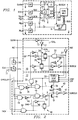
- Figure 1 is an electrical diagram, in block form, of an integrated circuit incorporating the preferred embodiment of the invention;
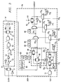
- Figure 2 is an electrical diagram, in schematic form, of a clock generator circuit;
- Figure 3 is an electrical diagram, in schematic form, of a delay stage in the clock generator circuit of Figure 2;
- Figures 4a and 4b are timing diagrams illustrating the operation of the clock generator circuit;
- Figure 5 is an electrical diagram, in block form, of another clock generator circuit;
- Figure 6 is an electrical diagram, in block form, of another clock generator circuit;
- Figure 7 is a timing diagram illustrating the operation of the circuit of Figure 6;
- Figure 8 is an electrical diagram, in block form of a clock generator circuit according to an embodiment of the invention;
- Figure 9 is a timing diagram illustrating the operation of the circuit of Figure 8;
- Figure 10 is an electrical diagram, in block form, of a clock generator circuit according to another embodiment of the invention;
- Figure 11 is a timing diagram illustrating the operation of the circuit of Figure 10;
- Figure 12 is an electrical diagram, in block form, of a clock generator circuit according to a further embodiment of the invention; and
- Figure 13 is a timing figure illustrating the operation of the circuit of Figure 12.
-
- Referring first to Figure 1, the construction of
integrated circuit 2, such as a microprocessor, math co-processor or the like having at least two different functions which can operate at different clock frequencies, and thus in which the preferred embodiment of the invention is implemented will be described. In this example, integratedcircuit 2 includes acore unit 4 which performs a sequence of instructions or some other complex logic operation, preferably at the fastest possible clock frequency to optimize circuit performance.Integrated circuit 2 further includesbus interface unit 6 which is in communication with input and output terminals (not shown) ofintegrated circuit 2, and is also in communication withcore unit 4 by way of internal bus IBUS.Bus interface unit 6 is intended to receive input signals presented at address and data input terminals, to control the operation ofcore unit 4 and other functions inintegrated circuit 2, and also to control the presentation of output data at output terminals; since the timing requirements ofbus interface unit 6 are governed by the input/output specifications of other integrated circuits in the system, it may require a slower clock frequency than that usable bycore unit 4. - For reference hereinbelow, certain of the input terminals to
integrated circuit 2 are illustrated in Figure 1 as being connected to circuitry via a bond wire W and a bond pad BP. Other inputs and outputs are, of course, similarly connected but are not shown in Figure 1 for purposes of clarity. The illustration of the bond pads BP in Figure 1 will become apparent relative to the optional wire bonding of one of the bond pads BP discussed hereinbelow. In addition, conventional input buffer circuits may also be provided withinintegrated circuit 2 in the conventional manner; such buffers are also not illustrated in Figure 1 for purposes of clarity. - In the example of Figure 1, integrated
circuit 2 is operable to receive an input clock signal at terminal CLKIN. The input clock signal may be an externally generated periodic clock, such as from an external oscillator, or alternatively the input clock signal may be generated on-chip based on a crystal connected to terminal CLKIN that determines the clock frequency.Clock control circuit 8 presents to core unit 4 (on line CORECLK) an internal clock signal at the same frequency as the input clock signal at terminal CLKIN, and presents to bus interface unit 6 (on line BUSCLK) an internal clock signal at one-half the frequency of the input clock signal received at terminal CLKIN. The half-frequency clock signal is generated and applied to line BUSCLK byfrequency divider 10, which in this case divides the input clock signal frequency by two prior to its presentation on line BUSCLK. - According to this arrangement,
clock control circuit 8 further includesclock generator 12 which receives the input clock signal from terminal CLKIN at a "set" input, and which receives the input clock signal from terminal CLKIN, delayed byprogrammable delay stage 14, at a "reset" input.Programmable delay stage 14 in this arrangement includes a default delay value that is enabled for normal (non-test mode) operation, implemented withinprogrammable delay stage 14 by the metallization pattern or by way of fusible links or other programmable elements (FAMOS transistors, etc.). In addition,programmable delay stage 14 also receives a test input from terminal TEST and j select lines 15j from selected input terminals IN0 through INn so that, in a special test mode selected by the logic state applied to terminal TEST, the j select lines 15j can select a portion of the delay period throughdelay stage 14. -
Programmable delay stage 14 andclock generator 12 each also receive an input on line 2XEN indicating if the clock doubling mode is to be enabled; when enabled, the clock doubling mode causes the core unit clock frequency on line CORECLK to be twice that of the bus clock frequency on line BUSCLK. In this example, selection of the clock doubling feature is made at the wire bonding step of the manufacturing process, by connecting the bond pad BP associated with line 2XEN to be connected to the Vcc power supply terminal (which, in this example, enables clock doubling) or to the Vss or ground terminal (disabling clock doubling). - As will be described hereinbelow,
clock control circuit 8 according to this arrangement is controlled by the state of line 2XEN, so that the clock signal on line CORECLK may be generated either in a clock doubling mode or in a non-clock doubling mode. In addition, interface circuitry controlling the communication of data on internal bus IBUS is also preferably controlled according to the state of line 2XEN, so that communication betweencore unit 4 andbus interface unit 6 can be performed according to the selected internal clock relationship. It is contemplated that the construction of such interface circuitry will be apparent to one of ordinary skill in the art having reference to this specification. - In the general sense,
clock generator 12 operates in the clock doubling mode to respond to one of the input clock signal edges; for purposes of this description, the term "rising edge" will refer to a low-to-high transition for a signal, and the term "falling edge" will refer to a high-to-low transition. In the example of Figure 1, the rising edge of the input clock signal sets the output of clock generator 12 (on line CORECLK) to a high level.Clock generator 12 resets low its output on line CORECLK responsive to receiving the rising edge of the input clock signal, delayed by the time delay set withinprogrammable delay stage 14. The delay period ofprogrammable delay stage 14 is preferably selected to slightly exceed the time required for the worst case clock phase in the instruction set or possible operations ofcore unit 4. As such,clock generator 12 uses edge triggered set and reset functions based on the input clock signal, and provides an internal clock signal on line CORECLK that is at the same frequency as the input clock signal at terminal CLKIN, at a fixed phase duration so that variations in the duty cycle of the input clock signal thus do not affect the duty cycle of the internal clock signal on line CORECLK. The delay period is preferably selected according to the propagation delay of the worst case logic path, thus ensuring proper operation ofintegrated circuit 2 regardless of the duty cycle of the input clock signal, and thus over a wide range of duty cycle timing specifications. - Meanwhile,
frequency divider 10 is generating a clock signal on line BUSCLK that is at half the frequency of the input clock signal at terminal CLKIN. Accordingly, the operation ofbus interface unit 6 can be controlled in a manner consistent with externally connected integrated circuits, while still allowing the operation ofcore unit 4 to perform at the highest practicable clock rate. - Referring now to Figure 2, the construction of
frequency divider 10 andclock generator 12 will now be described in detail. -
Frequency divider 10 in this example is of substantially conventional design, and includes a reset function by which its output may be suspended. Line CLKIN communicates the input clock signal (after buffering if desired) toinverters pass gates - Line RST communicates a reset signal from elsewhere in
integrated circuit 2 to an input ofNAND gate 22 infrequency divider 10 and to start/stop logic 30 inclock generator 12. Line RST is preferably buffered withinintegrated circuit 2, in the conventional manner, to eliminate false resets due to noise, and to ensure proper phase synchronisation after reset. The second input ofNAND gate 22 is connected to the output offrequency divider 10 on line BUSCLK. During non-reset modes, the low logic level on line RST presents a high logic level (via inverter 21) to one input ofNAND gate 22, allowing the state of line BUSCLK to control the output ofNAND gate 22. - The output of
NAND gate 22 is connected to one side ofpass gate 24. The other side ofpass gate 24 is received by latch 28 and communicated to one side of pass gate 26 (after inversion byinverter 27 to account for the inversion by latch 28). Latch 28, in this example and elsewhere, consists of a pair of cross-coupled inverters where the feedback inverter has significantly weaker drive than the feed-forward inverter so that it can be rapidly overwritten as a new logic level is received at its input; this weaker drive is illustrated in Figure 2 by an asterisk in the feedback inverter of latch 28 (and in other latches in Figures 2 and 3). - In this example, pass
gate 24 is operable to pass the state of the output ofNAND 22 to latch 28 during the low level phase of the input clock signal on line CLKIN. Accordingly, if line RST is low during this phase, the logical complement of the state of line BUSCLK is communicated to latch 28 during low phases of the input clock signal. After inversion byinverter 27, the state of latch 28 is communicated to passgate 26. -
Pass gate 26 has its other side connected to latch 20 which, viainverter 19, drives line BUSCLK. In this example, passgate 26 has its gates controlled by lines CLKt, CLKc in a complementary manner relative to passgate 24, such thatpass gate 26 is conductive during high level phases of the input clock signal at line CLKIN. Accordingly, the complement of the state of line BUSCLK thus requires both a low level phase and a high level phase to be communicated back to latch 20, for presentation (after inversion by inverter 19) on line BUSCLK as a logic level transition of this output clock. As such, the frequency at which line BUSCLK toggles will be exactly one-half that of the input clock signal at line CLKIN. - As noted above, when line RST is at a low logic level,
NAND gate 22 is operable to respond to the state of line BUSCLK; conversely, in a reset or suspend operation, where line RST is at a high logic level, the output ofNAND gate 22 is forced high regardless of the state of line BUSCLK. Accordingly, the state of line BUSCLK is held high during the reset condition. - Start/stop logic receives line RST (via inverter 21), line BUSCLK, and start and stop signals on lines STRT and STP, respectively. Start/
stop logic 30 includes such combinational logic as required to enable and disableclock generator 12 according to the reset condition on line RST, and according to the start and stop signals. The start and stop signals allow for suspension of the output clock signal on line CORECLK, as will be described hereinbelow. - The input clock signal at line CLKIN is communicated to an inverting input of
NAND gate 34 and to a non-inverting input ofNAND gate 36. The second input ofNAND gate 34 receives line 2XEN which enables clock doubling with a high logic level. The output ofNAND gate 34 is communicated, via invertingdelay stage 35, to the second input ofNAND gate 36. Delaystage 35 may consist of several inverters in series, of a conventional single delay stage, or other conventional delay circuits for delaying the propagation of the signal from the output ofNAND gate 34 to the input ofNAND gate 36 for a selected time. As a result,NAND gate 36 will present a low logic level pulse responsive to the rising edge of the input clock signal at line CLKIN, and having a pulse width corresponding to the propagation delay ofNAND gate 34 anddelay stage 35. The output ofNAND gate 36 is connected to the gate of a p-channel transistor 38 having its source-drain path connected between Vcc and the input oflatch 40; the output oflatch 40 drives line CORECLK viainverter 41. - The input clock signal on line CLKIN is also connected to fixed
delay stage 14f and variable delay stage 14v, connected in series. In this example, and as will be described in further detail hereinbelow, variable delay stage 14v receives inputs on line TEST and on jselect lines 15j, as shown in Figure 1. The output of variable delay stage 14v on line CLKDELAY is connected to a non-inverting input ofNAND gate 46 and to an inverting input ofNAND gate 44. The second input ofNAND gate 44 receives line 2XEN. As in the above-described case, the output ofNAND gate 44 is connected to a second input ofNAND gate 46 via invertingdelay stage 45. As a result, the output ofNAND gate 46 will present a low logic level pulse responsive to the rising edge of the signal on line CLKDELAY from variable delay stage 14v, having a pulse width defined by the delay throughNAND gate 44 anddelay stage 45. The output ofNAND gate 46 is connected, after inversion byinverter 47, to the gate of an n-channel transistor 42 having its source/drain path connected between the input oflatch 40 and ground. -
NAND gate 46 also receives an input from the output of start/stop logic 30, thus allowing the reset signal on line RST, and the start and stop signals on lines STRT and STP, to control the operation ofclock generator 12 in the clock doubling mode. For example, if start/stop logic 30 drives a low logic level at its output, the output ofNAND gate 46 will be forced high, ensuring that n-channel transistor 42 does not turn on. In such an event, latch 40 cannot be overwritten with a low level, thus disabling transitions of the clock signal on line CORECLK. - Line 2XEN is also connected to an inverting input of
NAND gate 50, which receives the input clock signal on line CLKIN at its other input. The output ofNAND gate 50 is connected to passgate 48 in complementary fashion (via inverter 49); as such,pass gate 48 is made non-conductive when line 2XEN is high, during the clock doubling mode. -
Clock generator 12 according to this example also can provide a half-frequency clock signal on line CORECLK during the non-clock doubling mode indicated by line 2XEN being at a low logic level.NAND gate 32 receives the output of latch 28 infrequency divider 10 at one input, and receives the output of start/stop logic 30 at the other input. Start/stop logic 30 is therefore able to gate the application of the output of latch 28 to the frequency divider portion ofclock generator 12, such as is useful in suspending its operation (as in the case of line RST being high for frequency divider 10) and restarting it in a synchronous manner. - The output of
NAND gate 32 is presented to one side ofpass gate 48. The opposite side ofpass gate 48 is coupled to the input oflatch 40. Considering the effect ofNAND gate 50 andinverter 49, the n-channel transistor inpass gate 48 receives a signal corresponding to the input clock signal on line CLKIN, and the p-channel transistor inpass gate 48 receives a signal corresponding to the logical complement of the input clock signal on line CLKIN; as such,pass gate 48 is gated similarly aspass gate 26 infrequency divider 10. As a result, in non-clock doubling mode,clock generator 12 is configured similarly as frequency divider 10 (with the two circuits sharing the first portion thereof ofNAND gate 22,pass gate 24 and latch 28), for generating a half-frequency clock on line CORECLK. In this mode, therefore, the frequency of the clock signal on lines CORECLK and BUSCLK are identical. - Figure 4a illustrates the operation of
clock generator 12 in clock doubling mode, selected by line 2XEN being at a high logic level. For purposes of clarity of description, small propagation delays and charging transients are not shown in Figure 4a. In this mode, a rising edge on line CLKIN first causes the output of NAND gate 36 (node S in Figure 4a) to go to a low logic level. This low logic level at the output ofNAND gate 36 continues until the rising edge propagates throughNAND gate 34 anddelay stage 35; this propagation delay is shown in Figure 4a as δ35, and defines the pulse width of the low logic level at node S. Responsive to node S being low,transistor 38 turns on, charging the input oflatch 40 high which, viainverter 41, drives line CORECLK high. Accordingly, in clock doubling mode the rising edge of the input clock signal operates to set the output ofclock generator circuit 12 on line CORECLK. - The rising edge of the input clock signal at line CLKIN also propagates through
delay stages 14f, 14v, appearing at line CLKDELAY after the delay period δ14 (i.e., the propagation delay throughdelay stages 14f, 14v). At such time as the rising edge of the input clock signal appears on line CLKDELAY, the output ofNAND gate 46 goes to a low logic level (the other inputs toNAND gate 46 being high). The low logic level at the output ofNAND gate 46, viainverter 47, drives the gate of n-channel transistor 42 (node R of Figures 2 and 4a) high, turning ontransistor 42 and discharging the input oflatch 40 to ground.Latch 40 andinverter 41, in turn, drive line CORECLK low in response totransistor 42 being turned on. Accordingly, the rising edge of the signal on line CLKDELAY operates to reset the output ofclock generator 12 on line CORECLK to a low level, delayed from the high level transition by the delay time δ14 ofprogrammable delay stage 14. - It should be apparent to one of ordinary skill in the art that the duration of the pulse width of the low logic level pulse at node S (i.e,. the time delay δ35) and the duration of the high logic level pulse at node R (i.e., the time delay δ45) should be selected to ensure that the input to latch 40 is fully charged and discharged, respectively, in each cycle. However, these delays should also be selected to prevent the set and reset pulses from overlapping, as such would cause a crowbar condition (i.e., direct short from Vcc to ground) through
transistors - As a result of the operation of
clock generator 12, a clock signal is generated on line CORECLK which is at the same frequency as the input clock signal, but which has a duty cycle independent from that of the input clock signal. This is because the duration of one of the phases of the clock on line CORECLK is dependent upon the time between the set and reset pulses (at low and high levels, respectively, in this example). According to this arrangement, the time between the set and reset pulses depends solely upon the delay period δ14 through programmable delay 14 (i.e., throughdelay stages 14f, 14v), and does not depend upon the duty cycle of the input clock signal on line CLKIN. Indeed, in the example of Figure 4a, it should be noted that the duration of the high level phase on line CORECLK is greater than that of the input clock signal on line CLKIN. As will be discussed in further detail hereinbelow, this allows the duty cycle of the internal high frequency clock on line CORECLK to be optimized for the worst case phase, rather than for an average which is dependent upon the input clock signal. - This independence of the duty cycle of the clock signal on line CORECLK is further evident from the later cycles (after time t2) shown in Figure 4a. In these cycles, the duty cycle of the input clock signal on line CLKIN after time t2 has become shorter than in the previous cycles illustrated in Figure 4a, to approximately half that of the desired duration on line CORECLK. As in the prior cycles, however, the rising edge of the signal on line CLKIN causes a low logic level pulse at node S which, in turn, drives line CORECLK high. After expiration of the delay period δ14 after this edge, line CLKDELAY presents a rising edge which causes node R to be driven high, driving line CORECLK low. As a result, the duty cycle of the clock signal on line CORECLK remains constant, as determined by the delay time δ14 of
programmable delay stage 14, and is thus independent of the duty cycle of the input clock signal on line CLKIN. - This construction of
clock generator 12 thus provides a high degree of stability in the generation of a high frequency internal clock based on a received high frequency input clock signal. Particularly as microprocessor clock frequencies increase to 25 MHz and beyond, the generation and presentation of external clock signals of high quality and stability becomes more difficult, especially considering ringing and other noise effects which become more pronounced with higher switching speeds. Sinceclock generator 12 generates its clock signals based on edges of the input clock signal, and on internal delays, the clock signal on line CORECLK is not strongly affected by noise and other instabilities in the input clock signal. - Referring next to Figure 4b, the operation of
clock generator 12 in the non-clock doubling mode, indicated by line 2XEN being at a low logic level, will now be described. With line 2XEN at a low logic level, the outputs ofNAND gates transistors HAND gate 50 to respond to the input clock signal on line CLKIN, so thatpass gate 48 receives complementary gating signals corresponding to line CLKIN. - The cycles illustrated in Figure 4b begin with the initial condition of line BUSCLK (and thus node IN20 at the input of latch 20) at a high logic level, and line CORECLK (and thus node IN40 at the input of latch 40) at a high logic level. Upon the falling edge of line CLKIN (corresponding to a rising edge on line CLKc and a falling edge on line CLKt),
pass gate 24 is made conductive, communicating the state of line BUSCLK, inverted byNAND 22, as a low logic level to node IN28 at the input to latch 28. This low logic level is also communicated via NAND gate 32 (the output of start/stop logic 30 being high to enable operation) as a low level (inverted twice by latch 28 and NAND gate 32) to node IN48 at the input to passgate 48. Passgates gate 24. - Upon the rising edge of the input clock signal, pass
gates gate 24 turns off. Latch 28 retains its low logic level input at this time due to the operation of its feedback inverter. Withpass gate 26 conductive, the state of node IN28 is communicated (after inversion by latch 28 and by inverter 27) to node IN20 at the input oflatch 20, thus presenting a low logic level on line BUSCLK. Similarly, withpass gate 48 conductive, the low logic level at node IN48 is communicated to the input of latch 40 (node IN40), and presented on line CORECLK. - This operation of
frequency divider 10 andclock generator 12 in the non-clock doubling mode continues, with the alternating state of line BUSCLK fed back throughNAND gate 22 intofrequency divider 10. As a result, in this mode the frequencies of the signals on lines BUSCLK and CORECLK are equal to each other, at half the frequency of the input clock signal frequency at line CLKIN. - As noted hereinabove relative to Figure 4a, the propagation delays through this circuit are not illustrated in Figure 4b, for clarity of description. However, for purposes of stability, it may be preferable to insert delay stages, such as inverter chains, at certain locations in the circuit, thus ensuring that a logic transition is not occurring at the input to a pass gate at the same time as the pass gate turns off. For example,
inverter 27 may be replaced by a series of inverters, with propagation delay there through as desired. - In addition,
clock generator 12 may be readily configured to provide a complementary clock signal to the signal on line CORECLK, for example by providing a similar circuit to that oflatch 40 andtransistors - According to this arrangement, the ability of
clock control circuit 8 to selectably operate in either the clock doubling mode or non-clock doubling mode, depending upon the state of line 2XEN, provides significant advantages in the design and operation ofintegrated circuit 2 over prior techniques. According to prior techniques, a control signal selected, for certain integrated circuit functions (such as the core unit and the bus interface unit), which of the clock signals was to control their operation; as such, the functional circuitry necessarily required relatively complex circuitry to implement this ability to respond to a selected clock signal, with such circuitry necessarily affecting the most critical timing path of the high frequency internal clocks. In this arrangement, however, the ability ofclock control circuit 8 to generate output clock signals in a selected mode allows the functional circuitry, such ascore unit 4, to be designed so that it need only respond to a single internal clock signal, as the determination of the core clock frequency is made byclock control circuit 8. - As noted above, the selection of which clock mode is made, in this example, by the bonding of pad 2XEN to a power supply or ground pad. This method of selecting the clock mode is especially beneficial to the manufacturer, as only a single type of
integrated circuit 2 need be fabricated in order to provide inventory for both types of products (clock doubled or not), as the selection of the operation mode need not be made at the initial wafer fabrication stage, but instead is determined in the packaging operation. Furthermore, the user ofintegrated circuit 2 is not required to make any provision, such as externally connecting a terminal high or low, in order to maintain the proper desired operating mode. - Referring back to the clock doubling mode of Figure 4a,
clock generator 12 thus generates an internal clock signal having a duty cycle which depends upon a delay time δ14 throughprogrammable delay stage 14. In modern high complexity integrated circuits such as microprocessors and math co-processors, one of the two clock phases will control the worst case logic propagation path, such that the duration of the worst case phase will be critical in the operation of the circuit (i.e., if the duration of this worst case clock phase is too short, the circuit will malfunction). As shown in Figure 2,programmable delay stage 14 preferably includes a fixeddelay stage 14f and a variable delay stage 14v, such that the delay time δ14, and thus the duration of the worst case clock phase, may be set or altered either during characterization, production test or in operation. - In setting delay time δ14, the circuit designer should consider, by way of modeling or other characterization, the worst case high speed logic path in
core unit 4 for a possible instruction or logic operation, and add to the time required for this worst case path (td) a certain safety margin time (tm) to arrive at a minimum clock phase duration ( - Referring now to Figure 3, a preferred construction of
programmable delay stage 14 will now be described. This construction ofprogrammable delay stage 14 includes such features as to provide a delay time δ14 that matches variations in voltage, temperature and processing which affect the minimum clock phase duration time th, and to provide the ability to readily change the delay time δ14 as necessary. -
Fixed delay stage 14f receives the input clock signal on line CLKIN viapass gate 59, controlled in complementary fashion by the signal on line 2XEN. In non-clock doubling mode (since the clock signal on line CLKDELAY is not used; see Figures 3 and 4b) with line 2XEN low,pass gate 59 is non-conductive; during clock doubling mode, passgate 59 remains conductive.Fixed delay stage 14f, according to the preferred construction, includes multiple delay elements of various logic types, selected according to the worst case propagation delay incore unit 4 or elsewhere incircuit 2. The use of multiple types of delay elements, rather than many delay elements of the same type (e.g., a string of inverters), provides a high degree of matching of the delay through fixeddelay stage 14f to variations of the worst case logic path resulting from changes in temperature, processing, and bias voltage, thus accounting for variations in the propagation delay among various types of circuit elements as a function of voltage, temperature, and process parameters. In this preferred construction, fixeddelay stage 14f includeslatch 52,inverter 53, NOR gate 54 (with another input tied to ground), three-input NAND gate 55 (with its two other inputs tied high), two-input NAND gate 56 (with its other input tied high), pass gate 57 (biased on), andcapacitors Capacitors core unit 4, and may be implemented as separate capacitors in fixeddelay stage 14f, or by way of parasitic capacitances therein. While one of each type of delay element is illustrated in Figure 3, fixeddelay stage 14f may include multiple ones of these elements, multiple chains of elements, or such other elements and combinations as useful to mimic the worstcase core unit 4 delay path. - Variable delay stage 14v, according to this preferred construction, receives the output of fixed
delay stage 14f, and adds a selectable amount of delay thereto, prior to presenting the result at its output on line CLKDELAY. Variable delay stage 14v in this preferred construction can select various delays in a special test mode, with a default delay set by way of metal mask options. In addition, as will be evident from the following description, the selection of the delay through variable delay stage 14v may be made in substantially equal increments by a binary code, thus allowing great flexibility in the selection of the overall delay time δ14. - In this example, variable delay stage 14v includes four individually selectable delay paths. The most significant delay path is a set of four inverter pairs 60 selectable by multiplexer 643. similarly, the next most significant delay path has two inverter pairs 60 selectable by multiplexer 642; with the next most significant delay path having one
inverter pair 60 selectable by multiplexer 641. Each of the inverter pairs 60 preferably has the same propagation delay there through (i.e., delay δ'). The least significant delay path is implemented by the connection ofcapacitor 61 bypass gate 62, adding a capacitive load which preferably matches one-half the delay δ' of aninverter pair 60, or the propagation delay of a single inverter. Accordingly, the delay time through variable delay stage 14v may be selected in a binary fashion, as the four selectable paths are weighted in a binary fashion (23, 22, 21, and 20 inverters, respectively). - Multiplexers 64 (and pass gate 62) cause the series path of the clock signal from fixed
delay stage 14f to either pass through associated delay elements, or pass directly to the next stage without being delayed, responsive to the control input applied thereto from multiplexers 703 through 700, respectively. Each of multiplexers 643, 642, 641, may be constructed as shown in Figure 3 for multiplexer 643. In this example, the source/drain path ofpass gate 66 is connected between the incoming clock signal and the input to the next stage, whilepass gate 68 has its source/drain path connected between the output of thefinal delay element 60 and the input to the next stage. Passgates inverters delay stage 14f (or from the prior multiplexer 64) is applied to the input of the next stage in variable delay stage 14v. The least significant delay stage ofcapacitor 61 is selected by the combination of apass gate 62 having its source/drain path connected betweencapacitor 61 and line CLKDELAY, and having its gates controlled in complementary fashion by the output of multiplexer 700. - Multiplexers 70 select between the value of a test signal input on an associated select line 15 or a default value, in communicating to multiplexer 64 (or pass gate 62) whether or not its associated delay value is to be included; multiplexers 70 are controlled by a signal indicating whether or not test mode is enabled. A default value is presented to each of multiplexers 70 by way of an associated weak inverter 77 having both its input and its output tied to a fixed voltage. For example, Figure 3 shows the inputs and outputs of each inverter 77 tied to Vcc, in which case inverters 77 will each drive a high voltage at their output. This state of each inverter 77 can be altered by opening the connection between its output and the fixed voltage by way of a metal mask, fuse, laser cut, or the like, allowing inverter 77 to drive its output to the opposite state. In the alternative, the default condition may be set by an electrically programmable element, a register bit, by software, or other conventional techniques.
- Each multiplexer 70, in this example, receives a select line 15 at one input, the output of inverter 77 at another input, and the output of
NAND gate 72 as the control input.NAND gate 72 receives line 2XEN at one input and line TEST at its other input. The output ofNAND gate 72 is connected to the gates of afirst pass gate 74 in complementary fashion (via inverter 73), and to the gates of asecond pass gate 76 in a manner complementary to its connection to passgate 74; as such, either passgate 74 or passgate 76 will be made conductive, depending upon the state of the output ofNAND gate 72. The output ofNAND gate 22 is also fed directly to the control input of the next multiplexer 70 in line. With the output ofNAND gate 72 low,pass gate 74 will be conductive and connects select line 15 to the control input of multiplexer 64 (or to passgate 62 in the case of multiplexer 700); a high output fromNAND gate 72 will makepass gate 76 conductive, connecting the output of inverter 77 to the control input of multiplexer 64 (or passgate 62 in the case of multiplexer 700). - In operation, in a non-clock doubling mode (line 2XEN low), the outputs of inverters 77 are selected by all multiplexers 70, presenting the default delay value, preventing metastable or indeterminate conditions in variable delay stage 14v. In clock doubling mode, the state of line TEST (at the other input of NAND gate 72) will control multiplexers 70. In a non-test mode, or normal operating mode, the output of the array of inverters 77 will determine the delay presented by variable delay stage 14v, ranging from no delay up to the propagation delay of fifteen inverters, selectable in single inverter (i.e., capacitor 61) increments in binary fashion by the four inverters 77.
- In test mode, the state of select lines 15 will determine the delay through variable delay stage 14v, in a binary fashion by the state of the four
select lines 15j. Test mode may be enabled by any one of the known techniques in the integrated circuit art, including the provision of a dedicated test mode terminal or pad, an overvoltage condition on one of the normal input terminals to the circuit, a special code executed bycircuit 2, or other known techniques. With line TEST high,pass gates 74 in multiplexers 70 will all be on, allowing the state of select lines 15 to determine the variable delay length. Accordingly, in this mode, one may operatecircuit 2 with varying delay times δ14 to determine the shortest delay time δ14, and thus the minimum clock phase duration (th) for whichcircuit 2 can still successfully operate under a given voltage or temperature condition. - It is contemplated that the provision of variable delay stage 14v, and its use during a test mode, will be of benefit primarily to the production and design engineers of a particular
integrated circuit 2. This is because initial prototype samples may be characterized in test mode to determine a minimum, yet safe, delay time δ14 for varying operating conditions and functions, thus allowing selection of the proper default value by opening the appropriate lines at the output of inverters 77 in variable delay stage 14v. Furthermore, the use of the test mode can allow for periodic measurement of the minimum delay time δ14 as thecircuit 2 is being produced, and accordingly for modification of the metallization mask setting the states of inverters 77 over time. - This construction of variable delay stage 14v may also be used, if desired, to individually set the state of inverter 77 for each functional circuit, for example by opening a polysilicon fuse at the output of each inverter 77 by way of a laser or an avalanche condition. Further in the alternative, the manufacturer of the circuit may be able to select the proper metal mask in process, based upon threshold voltages, channel lengths and other measurable parameters during the fabrication of
circuit 2. Of course, multiplexers 70 may further alternatively be responsive to a register location, such that the propagation delay through variable delay stage 14v can be set by software. - As a result of the foregoing teaching, therefore, the duration of the worst case clock phase depends upon a fixed value, closely matching variations in voltage, temperature and processing, plus a variable amount that can be readily selected. Accordingly, the generation of a high frequency (twice the bus clock frequency) internal clock generated from an external input clock signal which may have unstable duty cycle, and also the ability to tune and select the duty cycle of the internal clock so as to match variations in temperature and processing conditions, may be achieved. In particular, the internal clock so generated can be sufficiently stable relative to changes in the power supply voltages so as to enable the design and manufacture of high speed, high complexity logic circuits such as microprocessors, math co-processors and the like that can operate both at conventional (5 volt) power supply voltages a well as at low (3.3 volt) power supply voltages.
- The above-described arrangement is directed to the internal clock distribution system which generates a half-frequency clock for bus interface operations (line BUSCLK) and a high speed clock for core unit operations (line CORECLK) that is at the same frequency as the input clock signal. Of course, by including conventional frequency multipliers and other frequency synthesizer circuits, one may generate internal clock signals of higher or lower frequencies than that of the input clock signal. It is contemplated that one of ordinary skill in the art, having reference to this specification and the drawings, will be readily able to utilize the benefits of the foregoing teaching in such applications.
- Referring now to Figure 5, another clock generator circuit is illustrated in block form in which an internal clock signal is generated on line CORECLK at twice the frequency of the input clock signal. In this embodiment, the input clock signal on line CLKIN is communicated to edge
detector circuit 80, which generates a rising edge at its output to the set input ofclock generator 112 responsive to either a rising or falling edge on line CLKIN. Line CLKIN is also connected toprogrammable delay stage 114, constructed similarly asprogrammable delay stage 14 described hereinabove. The output ofprogrammable delay stage 114 on line CLKDELAY is connected to edgedetector 82, which detects either a rising or falling edge at its input and generates a rising edge at its output responsive to either a rising or falling edge on line CLKDELAY. The output ofedge detector 82 is connected to the reset input ofclock generator 112.Clock generator 112 is constructed similarly asclock generator circuit 12 described hereinabove. - In operation, each transition of the input clock signal on line CLKIN is detected by
edge detector 80, which applies a pulse at the set input ofclock generator 112 and, in this case, drives high the Q output ofclock generator 112 at line CORECLK. After elapse of the delay period δ114, the input clock transition will appear on line CLKDELAY and will be detected byedge detector 82 which, in turn, applies a pulse to the reset input ofclock generator circuit 112. The reset signal will drive line CORECLK at the Q output ofclock generator circuit 112 to a low logic level. Accordingly, since each transition (rising or falling) causes both a set pulse and a reset pulse to be applied toclock generator 112, the frequency at the output ofclock generator 112 will be at twice the frequency of the input clock signal. - Referring now to Figure 6, the construction of a clock multiplier arrangement will now be described. In the arrangement of Figure 6, the frequency of the clock signal on line CORECLK is again multiplied from that on line CLKIN; in this example, the frequency is doubled. Line CLKIN is received by rising
edge detector 84, constructed similarly asNAND gates delay stage 35 inclock generator 12 shown in Figure 2, to provide a pulse responsive to a rising edge of the signal on line CLKIN; in contrast to the arrangement of Figure 5, no pulse is generated by risingedge detector 84 responsive to a falling edge on line CLKIN. The output of risingedge detector 84 is connected to a first input ofOR gate 92. - Line CLKIN is also connected to a series of delay stages 214, 216, 218, each of which has a separate delay period (although one or more may have the same delay period, if desired). Delay stages 214, 216, 218 preferably include fixed and variable portions, as described hereinabove relative to
programmable delay stage 14. The output ofdelay stage 214 is connected to risingedge detector 86, which in turn has its output connected to one input ofOR gate 94. The output of delay stage 216 is connected to risingedge detector 88, which has its output connected to a second input ofOR gate 92. Similarly, the output ofdelay stage 218 is connected to the input of risingedge detector 90, which has its output connected to a second input ofOR gate 94. - OR
gate 92 drives the set input ofclock generator 212 with its output, whileOR gate 94 drives the reset input ofclock generator 212 with its output.Clock generator 212 may be constructed similarly asclock generators clock generator 12 presents a high logic level at its Q output, on line CORECLK, responsive to a pulse at its set input, and resets its Q output to a low logic level responsive to a pulse at its reset input. - According to the arrangement of Figure 6, therefore, the clock signal on line CORECLK is at twice the frequency of the input clock signal on line CLKIN, with the delay periods δ214, δ216, δ218 determining the duration of three successive phases in two cycles; the fourth phase in the second cycle is determined by the difference between the period of the input clock signal on line CLKIN and the sum of the delay periods δ214, δ216, δ218. Referring now to Figure 7, the operation of the arrangement of Figure 6 will now be described. As in the above cases, small propagation delays are not shown, for purposes of clarity.
- In Figure 7, the rising edge of line CLKIN is detected by rising
edge detector 84, which presents a high level pulse (OUT84 in Figure 7) to an input ofOR gate 92 and thus to the set input ofclock generator 212. Accordingly, this rising edge of line CLKIN initiates a rising edge of the clock signal on line CORECLK. After delay period δ214 has elapsed from the rising edge on line CLKIN, a rising edge is presented to risingedge detector 86, which issues a high level (OUT86) to ORgate 94 and thus to the reset input ofclock generator 212. This pulse fromOR gate 94 causesclock generator 212 to reset its Q output. As a result, the high level phase of the first cycle of the clock signal on line CORECLK is determined by the delay period δ214. - The rising edge of line CLKIN ripples next through delay stage 216 which, after delay time δ216, presents a rising edge to rising
edge detector 88. A pulse (see OUT88) is then presented to ORgate 92, to again causeclock generator 212 to present a high level at its Q output on line CORECLK. Accordingly, the delay time δ216 defines the duration of the low level phase of the first cycle of the clock signal on line CORECLK. - The rising edge next ripples through
delay stage 218, causing a rising edge to be presented, after an additional delay time δ218, to risingedge detector 90. Risingedge detector 90 then presents a pulse (see OUT90) to ORgate 94, sending a pulse to the reset input ofclock generator 212, resetting line CORECLK to a low logic level. Accordingly, the duration of the high level phase of the second cycle of the clock signal on line CORECLK is defined by the delay time δ218. - The Q output of
clock generator 212 on line CORECLK remains at a low logic level until the next rising edge of the input clock signal on line CLKIN is received. As such, the delay times δ214, δ216, δ218 must, of course, be selected so that their sum does not exceed the period of the input clock signal, as such a situation would result in an unstable clock on line CORECLK. The duration of the second low phase of the output clock signal on line CORECLK is thus defined by the difference in period in the input clock signal less the sum of the delay times δ214, δ216, δ218; this duration is shown in Figure 7 as time tLO. - The arrangement of Figure 6 thus provides for stable frequency multiplication, independent of the phase duration or duty cycle of the input clock signal, as the phase durations are defined by the delay times in the clock control circuit. As such, the duty cycle of the input clock may vary without affecting the duty cycle of the output clock signal, particularly since the falling edge of the input clock signal is not used in, and does not affect, the generation of the output clock signal. In addition, the delay times may be selected so that alternating output clock periods can have different phase durations. Furthermore, multiplication of the input clock frequency to other integral multiples (three and up) may be readily implemented, merely by stacking additional delay stages in a similar manner, so long as the sum of the delay times is less than the period of the input clock signal.
- The arrangements described hereinabove relative to Figures 5 and 6 may, of course, be used in conjunction with
frequency divider 10 or such other clock generator or frequency synthesizer circuits as useful. In addition, these alternative arrangements may also be constructed similarly as described hereinabove relative to Figure 2 to respond to the state of line 2XEN, or another control signal, so that the clock doubling mode may be selectably enabled or disabled. - Figures 8 and 9 illustrate a clock multiplier circuit according to an embodiment of the invention. In the arrangement of Figure 8, the frequency of the clock signal on line CORECLK is again multiplied from that on line CLKIN. In this embodiment, the frequency of CLKIN is doubled using only two delay stages 314a-b and three
active edge detectors 96a-c. For purpose of illustration,active edge detectors 96a-c will be assumed to be rising edge detectors. CLKIN is received by risingedge detector 96a, whose output is connected toOR gate 98. A clock generator, shown in Figure 8 as an SR (Set-Reset) flip-flop 312a, has its set input coupled to the output ofOR gate 98. The SR flip-flop shown in Figure 8 will output a high logic level after its set input (S) is set high and will maintain the high logic level until the reset input (R) is set high. After the reset input is set high, the SR flip-flop will output a low logic level until the set input is set high. The Q output of flip-flop 312a is the CORECLK signal. This signal is connected to delay stage 314a, constructed similarly toprogrammable delay stage 14 described hereinabove. The output of delay stage 314a is connected to rising edge detector 96b. The output of rising edge detector 96b is connected to the reset input offlip flop 312a and to one input of ANDgate 100. The output of risingedge detector 96a is also connected to the set input of SR flip-flop 312b. The Q output of SR flip-flop 312b (the "FIRST_CYCLE" signal) is coupled to the other input of ANDgate 100. The output of ANDgate 100 is connected to the set input of SR flip-flop 312c. The Q output of SR flip-flop 312c comprises the "FIRST_PH2" signal which is input to delaystage 314b. The output ofdelay stage 314b is input to risingedge detector 96c. The output of risingedge detector 96c is connected to the reset inputs of SR flip-flops OR gate 98. - The operation of the circuit of Figure 8 is best described in connection with the timing diagram of Figure 9. Upon receiving an active (in this case, rising) edge of signal CLKIN,
edge detector 96a outputs a pulse to one input ofOR gate 98, thereby driving its output high. This causes the Q output of SR flip-flop 312a to transition high, hence driving signal CORECLK high. The pulse generated by risingedge detector 96a also drives the set input of SR flip-flop 312b, causing the FIRST_CYCLE signal to transition high. The transition from low to high of CORECLK is delayed through delay stage 314a (by a time period of δ314a) and then detected by rising edge detector 96b. In response to receiving the delayed rising edge of CORECLK, rising edge detector 96b outputs a pulse to the reset input of SR flip-flop 312a and to ANDgate 100. In response to this pulse, SR flip-flop drives CORECLK low. Upon receiving the pulse from edge detector 96b, ANDgate 100 outputs a high pulse to the set input of SR flip-flop 312c, thereby driving the FIRST_PH2 signal high. Signal FIRST_PH2 is delayed bydelay stage 314b. Thereafter, the low-to-high transition of FIRST_PH2 is detected by risingedge detector 96c. In response,edge detector 96c outputs a pulse to the reset inputs of SR flip-flops OR gate 98. Consequently, signal CORECLK is driven high, signal FIRST_CYCLE is driven low and signal FIRST_PH2 is driven low. The low-to-high transition of CORECLK is delayed through delay stage 314a and detected by edge detector 96b. Once again, edge detector 96b causes the SR flip-flop 312a to drive CORECLK low. Since signal FIRST_CYCLE is low, the pulse received by ANDgate 100 from rising edge detector 96b does not affect SR flip-flop 312c. The circuit remains in this state, with CORECLK in a low logic state, FIRST_CYCLE in an low logic state and FIRST_PH2 in a low logic state, until the next active edge is received from the CLKIN signal. - This embodiment of the present invention provides essentially the same output signal as the circuit of Figure 6 with significantly less circuitry. In effect, SR flip-
flop 312b counts to "1" and then disables SR flip-flop 312c from generating additional clocks. The circuit shown in Figure 8 could be expanded to generate additional clocks responsive to an active CLKIN edge by setting the FIRST_CYCLE signal to "0" after counting a predetermined number of clock transitions. - Figures 10 and 11 illustrate another embodiment of the present invention, wherein the input clock signal CLKIN may be multiplied by a factor n, which may be stored in a register or hard-wired into the circuit. In the circuit of Figure 10, only two delay stages 414a-b and three
edge detectors 102a-c are used, regardless of the value of n. Signal CLKIN is input to edgedetector 102a, whose output is received by one input of ORgate 104. The output ofedge detector 102a is also connected to the reset input ofcounter 106. The output of ORgate 104 is coupled to set input of SR flip-flop 412, whose Q output comprises the CORECLK signal. The CORECLK signal is input to delay stage 414a whose output is connected to the input ofedge detector 102b. The output ofedge detector 102b is coupled to the reset input of SR flip-flop 412 and to the increment input ofcounter 106. The Q output of SR flip-flop 412 is received bydelay circuit 414b, whose output is coupled toedge detector 102c. The output ofedge detector 102c is coupled to one input of ANDgate 105. The output of ANDgate 105 is coupled to the other input of ORgate 104. The output ofcounter 106 is coupled to one input ofcomparator 107. The value n, which may be hard-wired or stored in a register, is present on the other input ofcomparator 107. If the value of the output ofcounter 106 is equal to the value of n, the output ofcomparator 107, the "match" signal, transitions high. The match signal is coupled to an inverted input of ANDgate 105. - The operation of the circuit of Figure 10 will be described using n=3. An active edge of the CLKIN signal causes the
edge detector 102a to generate a pulse which resets counter 106 and drives the set input of SR flip-flop 412 high, thereby causing a low-to-high transition of the CORECLK signal. Upon reset, thecounter 106 outputs a count of zero, thereby driving the match signal low (unless n = 0, which would be an inappropriate setting for the circuit). The low-to-high transition of CORECLK is input to edgedetector 102b after the delay through delay circuit 414a. When detected byedge detector 102b, a pulse is output to the reset input of SR flip-flop 412 and to the increment input ofcounter 106. Hence, this pulse causes CORECLK to driven low, CORECLK to be driven high and thecounter 106 to be incremented by "1". The low-to-high transition of CORECL K is detected byedge detector 102c after the delay caused bydelay stage 414b. In response,edge detector 102c outputs a pulse to ANDgate 105. Since the match signal is low, this pulse passes through ANDgate 105. The pulse output by ANDgate 105 passes through ORgate 104 to the set input of SR flip-flop 412. Consequently, CORECLK is driven high. As previously described, the low-to-high transition of CORECLK is delayed through delay stage 414a and detected byedge detector 102b which outputs a pulse to drive CORECLK low and to increment thecounter 106. Since the output ofcounter 106 now equals "2", the match signal remains low, and detection byedge detector 102c of the delayed low-to-high transition CORECLK drives the output of ANDgate 105 high, thereby causing a low-to-high transition of CORECLK. The low-to-high transition of CORECLK is delayed through delay stage 414a and detected byedge detector 102b which drives CORECLK low and increments thecounter 106 to a count of "3". A count of "3" causes a match incomparator 107, thereby driving the match signal high. A high match signal drives the output of ANDgate 105 low regardless of the output ofedge detector 102c. Therefore, the next pulse fromedge detector 102c caused by the low-to-high transition of CORECLK is blocked by ANDgate 105. Consequently, the CORECLK signal will remain in a low state until the next active edge of the CLKIN signal. - As can be seen, the number of clock cycles generated by SR flip-
flop 412 in response to each active edge of the CLKIN signal is dependent on the value of n. The delay caused by delay stage 414a sets the time of the high logic level phase of that CORECLK. The delay generated bydelay stage 414b sets the time of the low logic level phase of CORECLK except for the last low logic state which is determined not by thedelay stage 414b, but instead by the occurrence of the next active edge of the CLKIN signal. - Figures 12 and 13 illustrate a clock multiplying circuit using a
single delay stage 514 to multiply an input clock by a factor of n. This circuit operates similarly to the circuit of Figure 10, except thedelay stage 514 sets the times for both the high and low logic levels of output CORECLK. In operation,edge detector 108a detects the active edge of signal CLKIN. In response to detecting an active edge, 108a outputs a pulse to ORgate 104 which drives the set input of SR flip-flop 512 high, thereby driving the CORECLK signal high. The pulse also resetscounter 106. A low-to-high transition of CORECLK is delayed throughdelay stage 514 and input to fallingedge detector 108b and risingedge detector 108c. In response to the low-to-high transition of CORECLK,edge detector 108c outputs a pulse toincrement counter 106 and to drive the reset input of SR flip-flop 512 high, thereby driving CORECLK low. The match signal output fromcomparator 107 remains low until the value output fromcounter 106 equals the value n at the input of thecomparator 107. The high-to-low transition of CORECLK is detected by fallingedge detector 108b, after the delay caused bydelay stage 514. In response to detecting the high-to-low transition of CORECLK,edge detector 108b outputs a pulse to ANDgate 105. While the match signal is low, a pulse fromedge detector 108b generates a similar pulse on the output of ANDgate 105, which drives the set input of SR flip-flop 512 high, thereby causing a low-to-high transition of the CORECLK signal. - Hence, the falling
edge detector 108b detects a high-to-low transition of CORECLK after a delay specified by thedelay stage 514 and in response to such detection drives CORECLK high. Similarly, the risingedge detector 108c detects a low-to-high transition of CORECLK after the delay specified bydelay stage 514 and drives CORECLK low in response thereto. Upon each high-to-low transition detected by risingedge detector 108c, the counter increments. When the output of the counter equals n, the match signal is driven high, thereby blocking the next pulse to output from fallingedge detector 108b. Hence, CORECLK will remain in a low state until the next active edge of CLKIN, which resetscounter 106. - As can be seen, this circuit provides 50% duty cycle clocks using a
single delay stage 514. Hence, the amount of circuitry needed to implement the clock multiplier circuit can be greatly reduced. - The present invention can thus be implemented to provide significant advantages over conventional clock doubling schemes. First, the present invention provides for the generation of an internal clock, at the fundamental frequency of the input clock signal or at multiples thereof, having a phase duration which is independent of the duty cycle of the input clock signal. As such, instabilities in the duty cycle of the input clock signal, or noise effects such as ringing and the like, do not significantly affect the internal clock signals, even at high frequencies such as above 25 MHz. Furthermore, the phase duration of the internal clock signal can be optimized according to the worst case logic path within the circuit, so that erroneous operation is avoided even for unstable duty cycle input clocks. In addition, the generation of the optimized phase duration by way of a delay stage may be done in such a manner as to accurately match variations in temperature, voltage, and manufacturing parameters, and in such a manner as to allow characterization and adjustment thereof. It is therefore contemplated that the present invention will greatly facilitate the generation of internal clock signals in high frequency integrated circuits, particularly those that operate over a wide operating power supply voltage range.
- The clock multiplier factor n may be hard-wired or stored in a memory, such that the number of output clock cycles triggered in response to an active edge of the input clock can be varied without changing the circuit design. The clock multiplier can be implemented with as little as one delay circuit.
- While the invention has been described herein relative to its preferred embodiments, it is of course contemplated that modifications of, and alternatives to, these embodiments, such modifications and alternatives obtaining the advantages and benefits of this invention, will be apparent to those of ordinary skill in the art having reference to this specification and its drawings. For example, either rising or falling edges of the input clock, or both, could be used to generate the multiplied clock. Further, logic other than SR flip-flops could be used to generate the clock transitions responsive to the output of the edge detectors. Also, as shown herein, the circuitry for counting clock transitions may be implemented using a general purpose counter or by discrete logic. The number of transitions to be counted may vary depending upon which signals are blocked in response to detection of a desired count. It is contemplated that such modifications and alternatives are within the scope of the claimed invention.
Claims (17)
- Clock generating circuitry for generating output clock signals (CORECLK) responsive to an input clock signal (CLKIN), comprising:a resettable latch circuit (312a; 412; 512) for generating a sequence of output clock signal edges in response to the occurrence of a single active edge of said input clock signal;said latch circuit including a first input (S) coupled to receive a signal input from detection circuitry (96a; 102a; 108a) in response to detection of said active edge of the input clock signal thereby causing a first output transition in a first direction of said latch circuit;said latch output being coupled by a delay means (314a; 414; 514) and a first active edge detector (96b; 102b; 108c) to another input (R) of the latch circuit to apply a signal input to said another input causing a latch output transition in an opposite direction from said first direction in response to detection of an output transition in the first direction, after a predetermined delay provided by said delay means;circuitry including a delay means (314b; 414b; 514) coupled to a second active edge detector (96c; 102c; 108b) to detect delayed output transitions of said latch circuit in a predetermined direction and in response to each detected transition to apply a further input to said first input of the latch circuit after a respective delay increment, each said further input causing another output transition of the latch circuit in the first direction; andcircuitry (312b; 105-107) for inhibiting operation of said latch circuit after generation of a predetermined number of output clock signal edges.
- The clock generating circuitry of Claim 1, wherein each said delay means is provided by a common delay means (514) having an output coupled to each of said first and second active edge detectors (108c, 108b), and wherein one of said first and second active edge detectors is a rising edge detector (108c) and the other is a falling edge detector (108b).
- The clock generating circuitry of Claim 1 or Claim 2, wherein said inhibiting circuitry is reset responsive to the detection of an active edge of said input clock signal.
- The clock generating circuitry of any one of Claims 1 to 3, wherein said inhibiting circuitry includes counting circuitry (106) for counting output clock signal edges; and wherein said edge generating in said latch circuit is inhibited in response to a comparator output (MATCH) based on comparison of the count of the counting circuitry with a predetermined number (n).
- The clock generating circuitry of Claim 4 arranged so that the detection of said active edge of said input clock signal causes said counting circuitry to reset.
- The clock generating circuitry of any one of Claims 1 to 5 arranged so that the detection of said active edge of said input clock signal causes said latch circuit initially to set.
- The clock generating circuitry of Claim 1, wherein delayed outputs from said latch circuit are coupled to said first input of the latch circuit by a gating circuit (100, 312c, 314b, 96c; 105) that is disabled by said inhibiting circuitry (312b; 106, 107) after generation of said predetermined number of output clock signal edges.
- The circuitry of Claim 1 or Claim 2, wherein at least one of said predetermined delays is implemented by a plurality of logic elements, each corresponding to a different logic function (14f).
- The circuitry of Claim 1 or Claim 2, wherein at least one of said predetermined delays is implemented by a fixed delay stage (14f) in series with a variable delay stage (14v) comprising a plurality of delay elements (60); and a select circuit (641, 642, 643, 62) selecting among said plurality of delay elements to set the propagation delay of said variable delay stage.
- The circuitry of Claim 9, wherein said variable delay stage further comprises a plurality of programmable elements (77l) coupled to the select circuit of said variable delay stage (14v) and associated with each of said plurality of delay elements, each programmable element indicating whether or not its associated delay element is to be connected in series in said variable delay stage.
- The circuitry of any one of Claims 8 to 10, further comprising: a plurality of multiplexers (70), each having a first input coupled to an associated programmable element (77), each having a second input coupled to an associated select line (15), and each having a control input coupled to a test mode input (TEST) to select, responsive to said test mode input, either its associated select line or its associated programmable element for determining whether or not its associated delay element (60) is to be connected in series in said variable stage.
- A method of generating output clock signals (CORECLK) responsive to an input clock signal (CLKIN) by initiating a sequence comprising:operating a resettable latch circuit (312a; 412; 512) to generate a series of output clock signal edges in response to the occurrence of a single active edge of said input clock signal;applying a signal input to a first input (S) of said latch circuit in response to detection of said active edge of the input clock signal thereby causing a first output transition of said latch circuit in a first direction;after a predetermined delay causing a latch circuit output transition in an opposite direction from said first direction in response to detection by a first active edge detector (96b; 102b; 108c) of an output transition in the first direction, by applying a signal input to another input (R) of said latch circuit;and then in response to detection by a second active edge detector (96c; 102c; 108b) of an output transition of said latch circuit in a predetermined direction, applying a further input to said first input of the latch circuit after a predetermined delay to cause another output transition of said latch circuit in the first direction, to initiate repetition of said sequence;and inhibiting operation of said latch circuit after a selected number of repetitions of said sequence to generate a predetermined number of output clock signal edges.
- A method according to Claim 12, wherein a predetermined number of output clock signal edges is generated by counting said output clock signal edges (COUNT) and comparing the count with a reference number (n) and inhibiting repetition of said sequence on completion of said count.
- A method according to Claim 13, wherein the count is reset (RESET) in response to the detection of said active edge of the input clock signal.
- A method according to any one of Claims 12 to 14, wherein said sequence is repeated following inhibition of said sequence in response to a further input clock signal active edge.
- A method according to any one of Claims 12 to 14, wherein said predetermined delays are selectable.
- A method according to Claim 12 or Claim 16, wherein said predetermined delays are determined by delay stages comprising fixed (14f) and variable (14v) delay elements.
Applications Claiming Priority (6)
| Application Number | Priority Date | Filing Date | Title |
|---|---|---|---|
| US88075192A | 1992-05-08 | 1992-05-08 | |
| US880550 | 1992-05-08 | ||
| US07/880,550 US5336939A (en) | 1992-05-08 | 1992-05-08 | Stable internal clock generation for an integrated circuit |
| US880751 | 1992-05-08 | ||
| US07/975,809 US5359232A (en) | 1992-05-08 | 1992-11-13 | Clock multiplication circuit and method |
| US975809 | 1992-11-13 |
Publications (3)
| Publication Number | Publication Date |
|---|---|
| EP0570158A2 EP0570158A2 (en) | 1993-11-18 |
| EP0570158A3 EP0570158A3 (en) | 1994-06-22 |
| EP0570158B1 true EP0570158B1 (en) | 2000-01-19 |
Family
ID=27420503
Family Applications (1)
| Application Number | Title | Priority Date | Filing Date |
|---|---|---|---|
| EP19930303528 Expired - Lifetime EP0570158B1 (en) | 1992-05-08 | 1993-05-07 | Frequency multiplication circuit and method for generating a stable clock signal |
Country Status (3)
| Country | Link |
|---|---|
| EP (1) | EP0570158B1 (en) |
| JP (1) | JP3568215B2 (en) |
| DE (1) | DE69327612T2 (en) |
Cited By (3)
| Publication number | Priority date | Publication date | Assignee | Title |
|---|---|---|---|---|
| US6737901B2 (en) | 2001-10-08 | 2004-05-18 | Infineon Technologies Ag | Integrable, controllable delay device, delay device in a control loop, and method for delaying a clock signal using a delay device |
| US7123071B2 (en) | 2003-01-15 | 2006-10-17 | Infineon Technologies Ag | Method and device for producing delayed signals |
| EP3748855A4 (en) * | 2018-06-15 | 2021-01-20 | Mitsubishi Heavy Industries, Ltd. | SEMICONDUCTOR DEVICE |
Families Citing this family (16)
| Publication number | Priority date | Publication date | Assignee | Title |
|---|---|---|---|---|
| US5570294A (en) * | 1994-03-11 | 1996-10-29 | Advanced Micro Devices | Circuit configuration employing a compare unit for testing variably controlled delay units |
| US5430394A (en) * | 1994-03-11 | 1995-07-04 | Advanced Micro Devices, Inc. | Configuration and method for testing a delay chain within a microprocessor clock generator |
| US5617563A (en) * | 1994-11-04 | 1997-04-01 | Sony Corporation Of Japan | Duty cycle independent tunable clock |
| JP3505018B2 (en) * | 1994-11-22 | 2004-03-08 | 株式会社ルネサステクノロジ | Semiconductor integrated circuit |
| ATE156950T1 (en) * | 1995-05-05 | 1997-08-15 | Siemens Ag | CONFIGURABLE INTEGRATED CIRCUIT |
| JP3442924B2 (en) * | 1996-04-01 | 2003-09-02 | 株式会社東芝 | Frequency multiplier |
| DE19844481C1 (en) | 1998-09-28 | 2000-05-25 | Siemens Ag | Integrated circuit with operating mode selection pad |
| JP3883090B2 (en) * | 1999-02-17 | 2007-02-21 | 富士通株式会社 | Clock adjustment device for data recovery system |
| CA2270516C (en) * | 1999-04-30 | 2009-11-17 | Mosaid Technologies Incorporated | Frequency-doubling delay locked loop |
| US6671817B1 (en) * | 2000-03-15 | 2003-12-30 | Nortel Networks Limited | Method and apparatus for producing a clock signal having an initial state at reference point of incoming signal thereafter changing state after a predetermined time interval |
| US7126396B1 (en) * | 2003-07-16 | 2006-10-24 | National Semiconductor Corporation | System for clock duty cycle stabilization |
| JP2006217455A (en) * | 2005-02-07 | 2006-08-17 | Kawasaki Microelectronics Kk | Ring oscillator circuit |
| JP2008042501A (en) * | 2006-08-04 | 2008-02-21 | Nippon Telegr & Teleph Corp <Ntt> | Electronic circuit equipment |
| US7592844B2 (en) * | 2007-01-19 | 2009-09-22 | Power Integrations, Inc. | Comparator with complementary differential input stages |
| JP2009005029A (en) * | 2007-06-20 | 2009-01-08 | Nippon Telegr & Teleph Corp <Ntt> | Electronic circuit equipment |
| JP5486354B2 (en) * | 2010-03-08 | 2014-05-07 | ラピスセミコンダクタ株式会社 | Data transmission circuit |
Family Cites Families (4)
| Publication number | Priority date | Publication date | Assignee | Title |
|---|---|---|---|---|
| US4217639A (en) * | 1978-10-02 | 1980-08-12 | Honeywell Information Systems Inc. | Logic for generating multiple clock pulses within a single clock cycle |
| US4316148A (en) * | 1979-09-04 | 1982-02-16 | Sperry Corporation | Variable frequency logic clock |
| US4638256A (en) * | 1985-08-15 | 1987-01-20 | Ncr Corporation | Edge triggered clock distribution system |
| US5018111A (en) * | 1988-12-27 | 1991-05-21 | Intel Corporation | Timing circuit for memory employing reset function |
-
1993
- 1993-05-07 DE DE1993627612 patent/DE69327612T2/en not_active Expired - Lifetime
- 1993-05-07 EP EP19930303528 patent/EP0570158B1/en not_active Expired - Lifetime
- 1993-05-10 JP JP10815493A patent/JP3568215B2/en not_active Expired - Lifetime
Cited By (3)
| Publication number | Priority date | Publication date | Assignee | Title |
|---|---|---|---|---|
| US6737901B2 (en) | 2001-10-08 | 2004-05-18 | Infineon Technologies Ag | Integrable, controllable delay device, delay device in a control loop, and method for delaying a clock signal using a delay device |
| US7123071B2 (en) | 2003-01-15 | 2006-10-17 | Infineon Technologies Ag | Method and device for producing delayed signals |
| EP3748855A4 (en) * | 2018-06-15 | 2021-01-20 | Mitsubishi Heavy Industries, Ltd. | SEMICONDUCTOR DEVICE |
Also Published As
| Publication number | Publication date |
|---|---|
| EP0570158A2 (en) | 1993-11-18 |
| DE69327612T2 (en) | 2000-08-31 |
| JPH06202756A (en) | 1994-07-22 |
| EP0570158A3 (en) | 1994-06-22 |
| DE69327612D1 (en) | 2000-02-24 |
| JP3568215B2 (en) | 2004-09-22 |
Similar Documents
| Publication | Publication Date | Title |
|---|---|---|
| US5359232A (en) | Clock multiplication circuit and method | |
| US5336939A (en) | Stable internal clock generation for an integrated circuit | |
| EP0570158A2 (en) | A stable clock generator circuit with clock multiplication | |
| US6490207B2 (en) | Delay-locked loop with binary-coupled capacitor | |
| US4893271A (en) | Synthesized clock microcomputer with power saving | |
| US6292040B1 (en) | Internal clock signal generating circuit having function of generating internal clock signals which are multiplication of an external clock signal | |
| US5272729A (en) | Clock signal latency elimination network | |
| US6392458B1 (en) | Method and apparatus for digital delay locked loop circuits | |
| US10931289B2 (en) | DLL circuit having variable clock divider | |
| EP0162870B1 (en) | Synthesized clock microcomputer with power saving | |
| US6882196B2 (en) | Duty cycle corrector | |
| US10587253B1 (en) | Ring oscillator-based programmable delay line | |
| US6720673B2 (en) | Voltage island fencing | |
| US7015600B2 (en) | Pulse generator circuit and semiconductor device including same | |
| KR950010208B1 (en) | Phase-locked loop clock signal generator | |
| US5357204A (en) | One-shot clock generator circuit | |
| US5822596A (en) | Controlling power up using clock gating | |
| JP3233893B2 (en) | Delay locked circuit | |
| US7218156B2 (en) | Supply tracking clock multiplier | |
| US5923621A (en) | Clock doubler circuit with duty cycle control | |
| US5828257A (en) | Precision time interval division with digital phase delay lines | |
| JPH09512935A (en) | High precision clock distribution circuit | |
| EP0604126B1 (en) | Clock signal conditioning circuit | |
| US8625728B1 (en) | System and method for reducing electromagnetic interference and ground bounce in an information communication system by controlling phase of clock signals among a plurality of information communication devices | |
| US5945861A (en) | Clock signal modeling circuit with negative delay |
Legal Events
| Date | Code | Title | Description |
|---|---|---|---|
| PUAI | Public reference made under article 153(3) epc to a published international application that has entered the european phase |
Free format text: ORIGINAL CODE: 0009012 |
|
| AK | Designated contracting states |
Kind code of ref document: A2 Designated state(s): CH DE ES FR GB IE IT LI NL |
|
| PUAL | Search report despatched |
Free format text: ORIGINAL CODE: 0009013 |
|
| AK | Designated contracting states |
Kind code of ref document: A3 Designated state(s): CH DE ES FR GB IE IT LI NL |
|
| 17P | Request for examination filed |
Effective date: 19941219 |
|
| 17Q | First examination report despatched |
Effective date: 19960905 |
|
| GRAG | Despatch of communication of intention to grant |
Free format text: ORIGINAL CODE: EPIDOS AGRA |
|
| GRAG | Despatch of communication of intention to grant |
Free format text: ORIGINAL CODE: EPIDOS AGRA |
|
| GRAG | Despatch of communication of intention to grant |
Free format text: ORIGINAL CODE: EPIDOS AGRA |
|
| GRAH | Despatch of communication of intention to grant a patent |
Free format text: ORIGINAL CODE: EPIDOS IGRA |
|
| GRAH | Despatch of communication of intention to grant a patent |
Free format text: ORIGINAL CODE: EPIDOS IGRA |
|
| RAP1 | Party data changed (applicant data changed or rights of an application transferred) |
Owner name: NATIONAL SEMICONDUCTOR CORPORATION |
|
| GRAA | (expected) grant |
Free format text: ORIGINAL CODE: 0009210 |
|
| AK | Designated contracting states |
Kind code of ref document: B1 Designated state(s): CH DE ES FR GB IE IT LI NL |
|
| PG25 | Lapsed in a contracting state [announced via postgrant information from national office to epo] |
Ref country code: NL Free format text: LAPSE BECAUSE OF FAILURE TO SUBMIT A TRANSLATION OF THE DESCRIPTION OR TO PAY THE FEE WITHIN THE PRESCRIBED TIME-LIMIT Effective date: 20000119 Ref country code: LI Free format text: LAPSE BECAUSE OF FAILURE TO SUBMIT A TRANSLATION OF THE DESCRIPTION OR TO PAY THE FEE WITHIN THE PRESCRIBED TIME-LIMIT Effective date: 20000119 Ref country code: IT Free format text: LAPSE BECAUSE OF FAILURE TO SUBMIT A TRANSLATION OF THE DESCRIPTION OR TO PAY THE FEE WITHIN THE PRESCRIBED TIME-LIMIT;WARNING: LAPSES OF ITALIAN PATENTS WITH EFFECTIVE DATE BEFORE 2007 MAY HAVE OCCURRED AT ANY TIME BEFORE 2007. THE CORRECT EFFECTIVE DATE MAY BE DIFFERENT FROM THE ONE RECORDED. Effective date: 20000119 Ref country code: FR Free format text: LAPSE BECAUSE OF FAILURE TO SUBMIT A TRANSLATION OF THE DESCRIPTION OR TO PAY THE FEE WITHIN THE PRESCRIBED TIME-LIMIT Effective date: 20000119 Ref country code: ES Free format text: THE PATENT HAS BEEN ANNULLED BY A DECISION OF A NATIONAL AUTHORITY Effective date: 20000119 Ref country code: CH Free format text: LAPSE BECAUSE OF FAILURE TO SUBMIT A TRANSLATION OF THE DESCRIPTION OR TO PAY THE FEE WITHIN THE PRESCRIBED TIME-LIMIT Effective date: 20000119 |
|
| REG | Reference to a national code |
Ref country code: CH Ref legal event code: EP |
|
| REF | Corresponds to: |
Ref document number: 69327612 Country of ref document: DE Date of ref document: 20000224 |
|
| REG | Reference to a national code |
Ref country code: IE Ref legal event code: FG4D |
|
| EN | Fr: translation not filed | ||
| NLV1 | Nl: lapsed or annulled due to failure to fulfill the requirements of art. 29p and 29m of the patents act | ||
| REG | Reference to a national code |
Ref country code: CH Ref legal event code: PL |
|
| PLBE | No opposition filed within time limit |
Free format text: ORIGINAL CODE: 0009261 |
|
| STAA | Information on the status of an ep patent application or granted ep patent |
Free format text: STATUS: NO OPPOSITION FILED WITHIN TIME LIMIT |
|
| 26N | No opposition filed | ||
| REG | Reference to a national code |
Ref country code: GB Ref legal event code: 732E |
|
| REG | Reference to a national code |
Ref country code: GB Ref legal event code: IF02 |
|
| PGFP | Annual fee paid to national office [announced via postgrant information from national office to epo] |
Ref country code: IE Payment date: 20120525 Year of fee payment: 20 Ref country code: DE Payment date: 20120529 Year of fee payment: 20 |
|
| PGFP | Annual fee paid to national office [announced via postgrant information from national office to epo] |
Ref country code: GB Payment date: 20120525 Year of fee payment: 20 |
|
| REG | Reference to a national code |
Ref country code: DE Ref legal event code: R071 Ref document number: 69327612 Country of ref document: DE |
|
| REG | Reference to a national code |
Ref country code: GB Ref legal event code: PE20 Expiry date: 20130506 |
|
| PG25 | Lapsed in a contracting state [announced via postgrant information from national office to epo] |
Ref country code: DE Free format text: LAPSE BECAUSE OF EXPIRATION OF PROTECTION Effective date: 20130508 Ref country code: GB Free format text: LAPSE BECAUSE OF EXPIRATION OF PROTECTION Effective date: 20130506 |
|
| PG25 | Lapsed in a contracting state [announced via postgrant information from national office to epo] |
Ref country code: IE Free format text: LAPSE BECAUSE OF EXPIRATION OF PROTECTION Effective date: 20130507 |